NTE2934
MOSFET
N≠Channel, Enhancement Mode
High Speed Switch
Features:
D
Avalanche Rugged Technology
D
Rugged Gate Oxide Technology
D
Lower Input Capacitance
D
Improved Gate Charge
D
Extended Safe Operating Area
D
Lower R
DS
(on): 0.254
Typ
D
Lower Leakage Current: 10
µ
A (Max) @ V
DS
= 400V
Absolute Maximum Ratings:
Drain≠to≠Source Voltage, V
DSS
400V
. . . . . . . . . . . . . . . . . . . . . . . . . . . . . . . . . . . . . . . . . . . . . . . . . . . . .
Drain Current, I
D
Continuous
T
C
= +25
∞
C
11.5A
. . . . . . . . . . . . . . . . . . . . . . . . . . . . . . . . . . . . . . . . . . . . . . . . . . . . . . . . . . . . .
T
C
= +100
∞
C
7.3A
. . . . . . . . . . . . . . . . . . . . . . . . . . . . . . . . . . . . . . . . . . . . . . . . . . . . . . . . . . . . .
Pulsed (Note 1)
68A
. . . . . . . . . . . . . . . . . . . . . . . . . . . . . . . . . . . . . . . . . . . . . . . . . . . . . . . . . . . . . .
Total Power Dissipation (T
C
= +25
∞
C), P
D
92W
. . . . . . . . . . . . . . . . . . . . . . . . . . . . . . . . . . . . . . . . . . . .
Derate Above 25
∞
C
0.74W/
∞
C
. . . . . . . . . . . . . . . . . . . . . . . . . . . . . . . . . . . . . . . . . . . . . . . . . . . . . .
Gate≠Source Voltage, V
GS
±
30V
. . . . . . . . . . . . . . . . . . . . . . . . . . . . . . . . . . . . . . . . . . . . . . . . . . . . . . . . .
Single Pulsed Avalanche Energy (Note 2), E
AS
1134mJ
. . . . . . . . . . . . . . . . . . . . . . . . . . . . . . . . . . . . .
Avalanche Current (Note 1), I
AR
11.5A
. . . . . . . . . . . . . . . . . . . . . . . . . . . . . . . . . . . . . . . . . . . . . . . . . . . .
Repetitive Avalanche Energy (Note 1), E
AR
9.2mJ
. . . . . . . . . . . . . . . . . . . . . . . . . . . . . . . . . . . . . . . . . .
Peak Diode Recovery dv/dt (Note 3), dv/dt
4.0V/ns
. . . . . . . . . . . . . . . . . . . . . . . . . . . . . . . . . . . . . . . . .
Operating Junction Temperature Range, T
J
≠55
∞
to +150
∞
C
. . . . . . . . . . . . . . . . . . . . . . . . . . . . . . . . . .
Storage Temperature Range, T
stg
≠55
∞
to +150
∞
C
. . . . . . . . . . . . . . . . . . . . . . . . . . . . . . . . . . . . . . . . . .
Maximum Lead Temperature (During Soldering, 1/8" from case, 5sec), T
L
+300
∞
C
. . . . . . . . . . . . . .
Thermal Resistance, Junction≠to≠Case, R
thJC
1.35
∞
C/W
. . . . . . . . . . . . . . . . . . . . . . . . . . . . . . . . . . . .
Thermal Resistance, Junction≠to≠Ambient, R
thJA
40
∞
C/W
. . . . . . . . . . . . . . . . . . . . . . . . . . . . . . . . . . . .
Note 1. Repetitive Rating: Pulse width limited by maximum junction temperature.
Note 2. L = 15mH, I
AS
= 11.5A, V
DD
= 50V, R
G
= 27
, Starting T
J
= +25
∞
C.
Note 3. I
SD
17A, di/dt
250A/
µ
s, V
DD
V
(BR)DSS
, Starting T
J
= +25
∞
C.
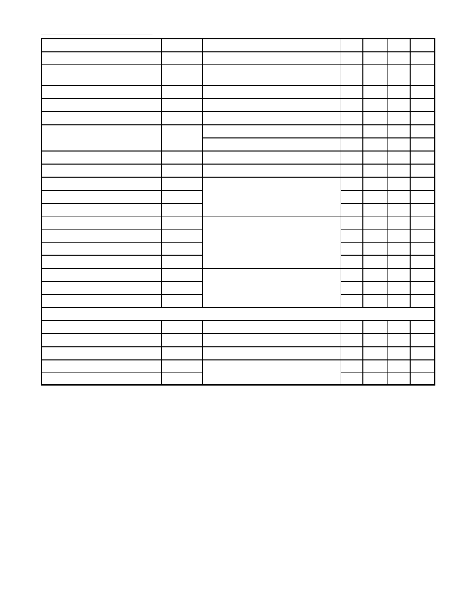
Electrical Characteristics: (T
C
= +25
∞
C unless otherwise specified)
Parameter
Symbol
Test Conditions
Min
Typ
Max
Unit
Drain≠Source Breakdown Voltage
BV
DSS
V
GS
= 0V, I
D
= 250
µ
A
400
≠
≠
V
Breakdown Voltage Temperature
Coefficient
V
(BR)DSS
/
T
J
I
D
= 250
µ
A
≠
0.46
≠
V/
∞
C
Gate Threshold Voltage
V
GS(th)
V
DS
= 5V, I
D
= 250
µ
A
2.0
≠
4.0
V
Gate≠Source Leakage Forward
I
GSS
V
GS
= 30V
≠
≠
100
nA
Gate≠Source Leakage Reverse
I
GSS
V
GS
= ≠30V
≠
≠
≠100
nA
Drain≠to≠Source Leakage Current
I
DSS
V
DS
= 400V
≠
≠
10
µ
A
V
DS
= 320V, T
C
= +125
∞
C
≠
≠
100
µ
A
Static Drain≠Source ON Resistance
R
DS(on)
V
GS
= 10V, I
D
= 5.75A, Note 4
≠
≠
0.3
Forward Transconductance
g
fs
V
DS
= 50V, I
D
= 5.75A, Note 4
≠
9.75
≠
mhos
Input Capacitance
C
iss
V
GS
= 0V, V
DS
= 25V, f = 1MHz
≠
2140
2780
pF
Output Capacitance
C
oss
≠
305
350
pF
Reverse Transfer Capacitance
C
rss
≠
134
155
pF
Turn≠On Delay Time
t
d(on)
V
DD
= 200V
,
I
D
= 17A, R
G
= 6.2
,
≠
20
50
ns
Rise Time
t
r
Note 4, Note 5
≠
22
55
ns
Turn≠Off Delay Time
t
d(off)
≠
100
210
ns
Fall Time
t
f
≠
32
75
ns
Total Gate Charge
Q
g
V
GS
= 10V, I
D
= 17A, V
DS
= 320V,
≠
101
131
nC
Gate≠Source Charge
Q
gs
Note 4, Note 5
≠
14
≠
nC
Gate≠Drain ("Miller") Charge
Q
gd
≠
51.5
≠
nC
Source≠Drain Diode Ratings and Characteristics
Continuous Source Current
I
S
(Body Diode)
≠
≠
11.5
A
Pulse Source Current
I
SM
(Body Diode) Note 1
≠
≠
68
A
Diode Forward Voltage
V
SD
T
J
= +25
∞
C, I
S
= 11.5A, V
GS
= 0V, Note 4
≠
≠
1.5
V
Reverse Recovery Time
t
rr
T
J
= +25
∞
C, I
F
= 17A, di
F
/dt = 100A/
µ
s,
≠
385
≠
ns
Reverse Recovery Charge
Q
rr
Note 4
≠
4.85
≠
µ
C
Note 1. Repetitive Rating: Pulse width limited by maximum junction temperature.
Note 4. Pulse Test: Pulse Width = 250
µ
s, Duty Cycle
2%.
Note 5. Essentially independent of operating temperature.