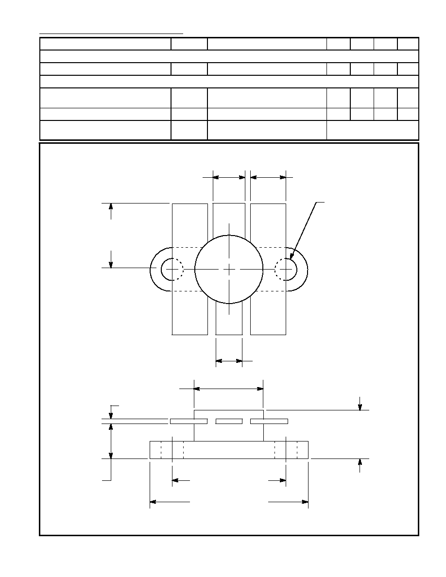
NTE352
Silicon NPN Transistor
RF Power Amp, Driver
Description:
The NTE352 is a silicon NPN transistor in a W65 type package designed primarily for use in 12.5V
VHF large≠signal power amplifier applications required in commercial and industrial FM equipment
to 175MHz.
Features:
D
Specified 12.5V, 175MHz Characteristics:
Output Power = 75W
Minimum Gain = 7.0dB
Efficiency = 55%
D
Characterized with Series Equivalent large≠Signal Impedance Parameters
D
Internal Matching Network Optimized for Minimum Gain Frequency Slope Response over the
Range 136 to 175MHz
D
Load Mismatch capability at Rated P
OUT
and Supply Voltage
Absolute Maximum Ratings:
Collector≠Emitter Voltage, V
CEO
18V
. . . . . . . . . . . . . . . . . . . . . . . . . . . . . . . . . . . . . . . . . . . . . . . . . . . . . .
Collector≠Base Voltage, V
CBO
36V
. . . . . . . . . . . . . . . . . . . . . . . . . . . . . . . . . . . . . . . . . . . . . . . . . . . . . . .
Emitter≠Base Voltage, V
EBO
4V
. . . . . . . . . . . . . . . . . . . . . . . . . . . . . . . . . . . . . . . . . . . . . . . . . . . . . . . . . .
Collector Current (Peak), I
C
20A
. . . . . . . . . . . . . . . . . . . . . . . . . . . . . . . . . . . . . . . . . . . . . . . . . . . . . . . . . .
Total Device Dissipation (Note 1, T
C
= +25
∞
C), P
D
250W
. . . . . . . . . . . . . . . . . . . . . . . . . . . . . . . . . . . .
Derate Above 25
∞
C
1.43mW/
∞
C
. . . . . . . . . . . . . . . . . . . . . . . . . . . . . . . . . . . . . . . . . . . . . . . . . . . .
Storage Temperature Range, T
stg
≠65
∞
to +150
∞
C
. . . . . . . . . . . . . . . . . . . . . . . . . . . . . . . . . . . . . . . . . .
Thermal Resuistance, Junction≠to≠Case (Note 2), R
thJC
0.7
∞
C/W
. . . . . . . . . . . . . . . . . . . . . . . . . . . .
Note 1. This device is designed for RF operation. The total device dissipation rating applies only
when the device is operated as an RF amplifier.
Note 2. Thermal Resistance is determined under specified RF operating conditions by infrared
measurement techniques.
Electrical Characteristics: (T
C
= +25
∞
C unless otherwise specified)
Parameter
Symbol
Test Conditions
Min
Typ
Max
Unit
OFF Characteristics
Collector≠Emitter Breakdown Voltage
V
(BR)CEO
I
C
= 100mA, I
B
= 0
18
≠
≠
V
V
(BR)CES
I
C
= 50mA, V
BE
= 0
36
≠
≠
V
Emitter≠Base Breakdown Voltage
V
(BR)EBO
I
E
= 10mA, I
C
= 0
4
≠
≠
V
ON Characteristics
DC Current Gain
h
FE
I
C
= 5A, V
CE
= 5V
10
75
150