 | –≠–ª–µ–∫—Ç—Ä–æ–Ω–Ω—ã–π –∫–æ–º–ø–æ–Ω–µ–Ω—Ç: NTE3882 | –°–∫–∞—á–∞—Ç—å:  PDF PDF  ZIP ZIP |
NTE3882
Integrated Circuit
NMOS, Counter Timer Control (CTC)
Description:
The NTE3882 Counter Timer Circuit (CTC) is a programmable, four channel device in a 28≠Lead DIP
type package that provides counting and timing functions for the NTE3880. The NTE3880 configures
the NTE3882's four independent channels to operate under various modes and conditions as
required.
The internal structure of the NTE3882 consists of an NTE3880 bus interface, internal control logic,
four counter channels, and interrupt control logic. Each channel has an interrupt vector for automatic
interrupt vectoring, and interrupt priority is determined by channel number with channel
having the
highest priority.
The channel logic is composed of 2 registers, 2 counters and control logic. The registers include and
8≠bit time constant register and an 8≠bit channel control register. The counters include as 8≠bit read-
able down counter and an 8≠bit prescaler. The prescaler may be programmed to divide the system
clock by either 16 or 256.
Structure:
D
N≠Channel Silicon Gate Depletion Load Technology
D
Single 5V Supply
D
Single Phase 5V Clock
D
Four Independent Programmable 8≠Bit Counter/16≠Bit Timer Channels
Features:
D
Each Channel may be Selected to Operate in Either a Counter Mode or Timer Mode
D
Programmable Interrupts on Counter or Timer States
D
A Time Constant Register Automatically Reloads, the Down Counter at Zero and the Cycle is
Repeated
D
Readable Down Counter Indicates Number of Counts≠to≠Go until Zero
D
Selectable 16 or 256 Clock Prescaler for Each Timer Channel
D
Selectable Positive or Negative Trigger may Initiate Timer Operation
D
Three Channels have Zero Count/Timeout Outputs capable of Driving Darlington Transistors
D
Daisy Chain Priority Interrupt Logic Included to Provide for Automatic Interrupt Vectoring without
External Logic
D
All Inputs and Outputs Fully TTL Compatible
Absolute Maximum Ratings:
Temperature Under Bias
0
∞
to +70
∞
C
. . . . . . . . . . . . . . . . . . . . . . . . . . . . . . . . . . . . . . . . . . . . . . . . . . . . .
Storage Temperature Range
≠65
∞
to +150
∞
C
. . . . . . . . . . . . . . . . . . . . . . . . . . . . . . . . . . . . . . . . . . . . . . .
Voltage On Any Pin With Respect to GND
≠0.3V to +7V
. . . . . . . . . . . . . . . . . . . . . . . . . . . . . . . . . . . . .
Power Dissipation
0.8W
. . . . . . . . . . . . . . . . . . . . . . . . . . . . . . . . . . . . . . . . . . . . . . . . . . . . . . . . . . . . . . . . .
Note 1. Stresses above those listed under "Absolute Maximum Ratings" may cause permanent
damage to the device. This is a stress rating only functional operation of the device at these
or any other condition above those indicated in the operational sections of this specification
is not implied. Exposure to absolute maximum rating conditions for extended periods may
affect device reliability.
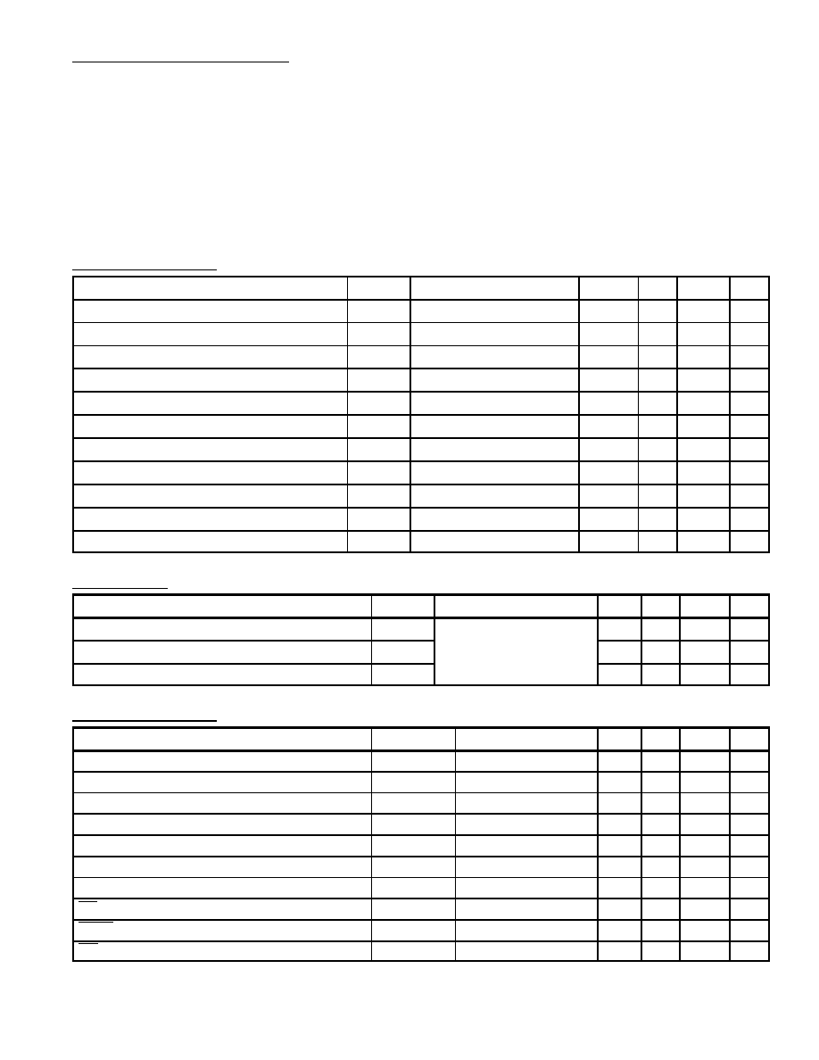
DC Characteristics: (T
A
= 0
∞
to 70
∞
C, V
CC
= 5V
±
5% unless otherwise specified)
Parameter
Symbol
Test Conditions
Min
Typ
Max
Unit
Clock Input Low Voltage
V
ILC
≠0.3
≠
0.45
V
Clock Input High Voltage
V
IHC
V
CC
≠0.6
≠
V
CC
+3
V
Input Low Voltage
V
IL
≠0.3
≠
0.8
V
Input High Voltage
V
IH
2.0
≠
V
CC
V
Output Low Voltage
V
OL
I
OL
= 2mA
≠
≠
0.4
V
Output High Voltage
V
OH
I
OH
= ≠250
µ
A
2.4
≠
≠
V
Power Supply Current
I
CC
T
C
= 250ns
≠
≠
120
mA
Input Leakage Current
I
L1
V
IN
= 0 to V
CC
≠
≠
10
µ
A
Tri≠State Output Leakage Current in Float
I
LOH
V
OUT
= 2.4 to V
CC
≠
≠
10
µ
A
Tri≠State Output Leakage Current in Float
I
LOL
V
OUT
= 0.4V
≠
≠
≠10
µ
A
Darlington Drive Current
I
OHD
V
OH
= 1.5V, R
EXT
= 390
≠1.5
≠
≠
mA
Capacitance: (T
A
= +25
∞
C, f = 1MHz unless otherwise specified)
Parameter
Symbol
Test Conditions
Min
Typ
Max
Unit
Clock Capacitance
C
Unmeasured Pins
≠
≠
20
pF
Input Capacitance
C
IN
Returned to GND
≠
≠
5
pF
Output Capacitance
C
OUT
≠
≠
10
pF
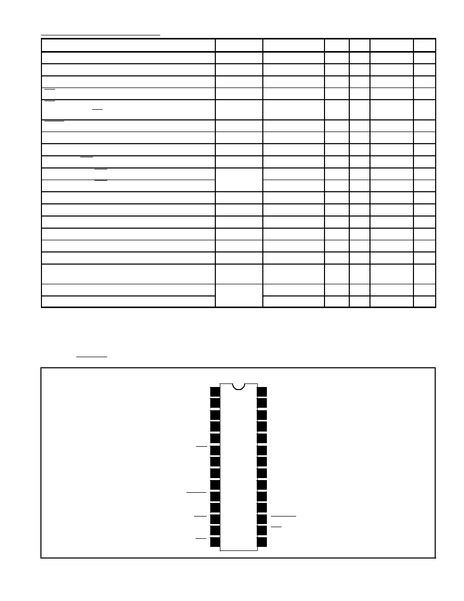
AC Characteristics: (T
A
= 0
∞
to 70
∞
C, V
CC
= 5V
±
5% unless otherwise specified)
Parameter
Symbol
Test Conditions
Min
Typ
Max
Unit
Clock Cycle Time
TcC
400
≠
Note 2
ns
Clock Width (High)
TwCH
170
≠
2000
ns
Clock Width (Low)
TwCL
170
≠
2000
ns
Clock Fall Time
TfC
≠
≠
30
ns
Clock Rise Time
TrC
≠
≠
30
ns
All Hold Times
Th
0
≠
≠
ns
CS to Clock
Setup Time
TsCS(C)
250
≠
≠
ns
CE to Clock
Setup Time
TsCE(C)
200
≠
≠
ns
IORQ
to Clock
Setup Time
TsIO(C)
250
≠
≠
ns
RD to Clock
Setup Time
TsRD(C)
240
≠
≠
ns
Note 2. TcC = TwCH + TwCL + TcC + TrC.
AC Characteristics (Cont'd): (T
A
= 0
∞
to 70
∞
C, V
CC
= 5V
±
5% unless otherwise specified)
Parameter
Symbol
Test Conditions
Min
Typ
Max
Unit
Clock
to Data Out Delay
TdC(DO)
Note 3
≠
≠
240
ns
Clock
to Data Out Float Delay
TdC(DOz)
≠
≠
230
ns
Data In to Clock
Setup Time
TsDI(C)
60
≠
ns
M1 to Clock
Setup Time (INTA or M1 Cycle)
TsM1(C)
210
≠
≠
ns
M1
to IEO
Delay (Interrupt Immediately
Preceding M1)
TdM1(IEO)
Note 4, Note 5
≠
≠
300
ns
IORQ
to Data Out Delay (INTA Cycle)
TdIO(DOT)
Note 3
≠
≠
340
ns
IEI
to IEO
Delay
TdIEI(IEOf)
Note 4
≠
≠
190
ns
IEI
to IEO
Delay (After ED Decode)
TdIEI(IEOr)
Note 4
≠
≠
220
ns
Clock
to INT
Delay
TdC(INT)
Timer Mode
≠
≠
TcT + 220
ns
CLR/TRG
to INT
(TsCTR(C) Satisfied)
TdCTK(INT)
Counter Mode
≠
≠
TcC + 230
ns
CLR/TRG
to INT
(TsCTR(C) Not Satisfied)
≠
≠
2TcC + 530
ns
CLK Cycle Time
TcCTR
Counter Mode
2TcC
≠
≠
ns
CLK/TRG Rise Time
TrCTR
≠
≠
50
ns
CLK/TRG Fall Time
TfCTR
≠
≠
50
ns
CLK/TRG Width (Low)
TwCTRL
200
≠
≠
ns
CLK/TRG Width (High)
TwCTRH
200
≠
≠
ns
CLK
to Clock
Setup Time for Immediate Count
TsCTR(Cc)
Counter Mode
300
≠
≠
ns
TRG
to Clock
Setup Time for Enabling of
Prescaler on Following Clock
TsCTR(Ct)
Timer Mode
210
≠
≠
ns
Clock
to ZC/TO
Delay
TdC(ZCTOr)
260
≠
≠
ns
Clock
to ZC/TO
Delay
190
≠
≠
ns
Note 3. Increase delay by 10ns for each 50pF increase in loading, 200pF maximum for data lines
and 100pF for control lines.
Note 4. Increase delay by 10ns for each 10pF increase in loading, 100pF maximum.
Note 5. 2.5 TcC > (N≠2) TdIEI(IEOF) + TdIM1(IEO) + TsIEI(IO).
Note 6. RESET must be active for a minimum of 3 clock cycles.
CE
CS
0
CS
1
RESET
CLK/TRG
3
CLK/TRG
2
CLK/TRG
1
CLK/TRG
0
D
0
D
1
D
2
D
3
M1
INT
IORQ
RD
Pin Connection Diagram
16
System Clock Input
IEO
(+) 5V
1
2
3
4
5
GND
6
7
8
28
27
26
25
24
23
22
21
9
20
10
11
19
18
12
17
13
IEI
14
15
D
4
D
5
D
6
D
7
ZC/TO
0
ZC/TO
1
ZC/TO
2
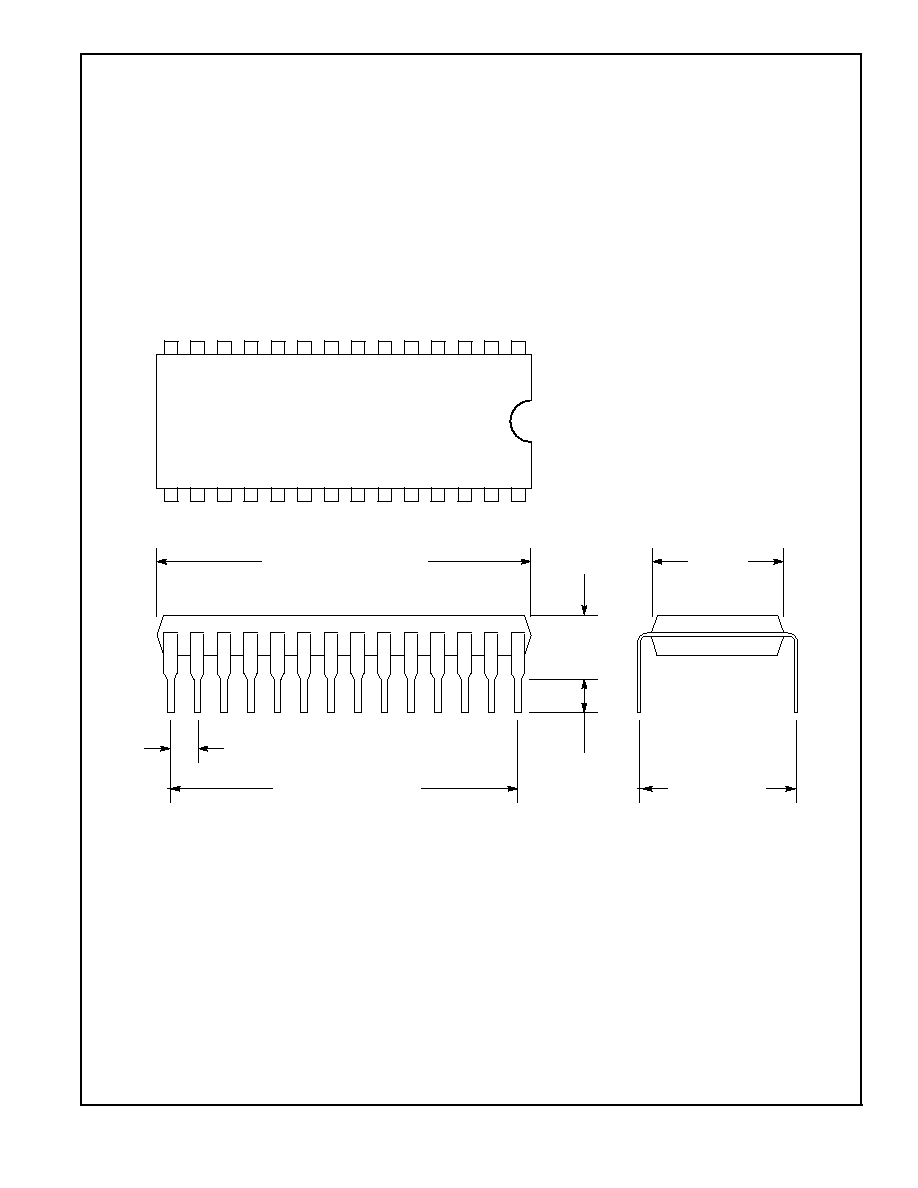
1.469 (37.32) Max
1.300 (33.02)
.540
(13.7)
.600
(15.24)
.250
(6.35)
.122
(3.1)
Min
.100 (2.54)
15
28
14
1