NTE56051 & NTE56052
TRIAC, 8A Low Logic Level
Description:
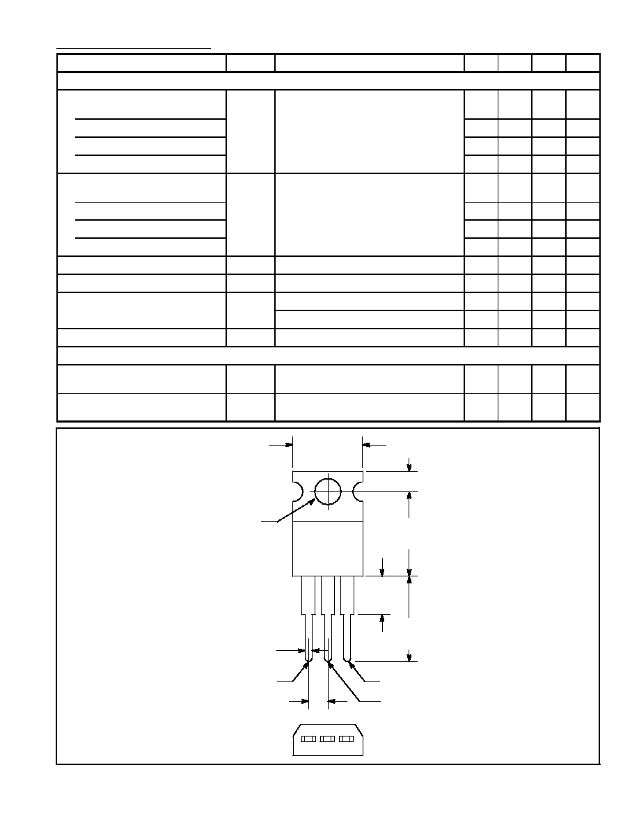
The NTE56051 and NTE56052 are glass passivated, Low Logic Level TRIACs in a TO220 type pack-
age designed for use in general purpose bidirectional switching and phase control applications.
These devices are intended to be interfaced directly to microcontrollers, logic integrated circuits, and
other low power gate trigger circuits.
Absolute Maximum Ratings:
Repetitive Peak Off≠Sate Voltage (Note 1), V
DRM
NTE56051
500V
. . . . . . . . . . . . . . . . . . . . . . . . . . . . . . . . . . . . . . . . . . . . . . . . . . . . . . . . . . . . . . . . .
NTE56052
600V
. . . . . . . . . . . . . . . . . . . . . . . . . . . . . . . . . . . . . . . . . . . . . . . . . . . . . . . . . . . . . . . . .
RMS On≠State Current (Full Sine Wave, T
MB
102
∞
C), I
T
(RMS)
8A
. . . . . . . . . . . . . . . . . . . . . . . . . .
Non≠Repetitive Peak On≠State Current, I
TSM
(Full Sine Wave, T
J
= +125
∞
C prior to Surge, with Reapplied V
DRM
max)
t = 20ms
55A
. . . . . . . . . . . . . . . . . . . . . . . . . . . . . . . . . . . . . . . . . . . . . . . . . . . . . . . . . . . . . . . . .
t = 16.7ms
60A
. . . . . . . . . . . . . . . . . . . . . . . . . . . . . . . . . . . . . . . . . . . . . . . . . . . . . . . . . . . . . . . .
I
2
t for Fusing (t = 10ms), I
2
t
15A
2
sec
. . . . . . . . . . . . . . . . . . . . . . . . . . . . . . . . . . . . . . . . . . . . . . . . . . . . . .
Repetitive Rate≠of≠Rise of On≠State Current after Triggering, dI
T
/dt
(I
TM
= 12A, I
G
= 0.2A, dI
G
/dt = 0.2A/
µ
s)
MT
2
(+), G (+)
50A/
µ
s
. . . . . . . . . . . . . . . . . . . . . . . . . . . . . . . . . . . . . . . . . . . . . . . . . . . . . . . . .
MT
2
(+), G (≠)
50A/
µ
s
. . . . . . . . . . . . . . . . . . . . . . . . . . . . . . . . . . . . . . . . . . . . . . . . . . . . . . . . . .
MT
2
(≠), G (≠)
50A/
µ
s
. . . . . . . . . . . . . . . . . . . . . . . . . . . . . . . . . . . . . . . . . . . . . . . . . . . . . . . . . .
MT
2
(≠), G (+)
10A/
µ
s
. . . . . . . . . . . . . . . . . . . . . . . . . . . . . . . . . . . . . . . . . . . . . . . . . . . . . . . . . .
Peak Gate Current, I
GM
2A
. . . . . . . . . . . . . . . . . . . . . . . . . . . . . . . . . . . . . . . . . . . . . . . . . . . . . . . . . . . . . .
Peak Gate Voltage, V
GM
5V
. . . . . . . . . . . . . . . . . . . . . . . . . . . . . . . . . . . . . . . . . . . . . . . . . . . . . . . . . . . . .
Peak Gate Power, P
GM
5W
. . . . . . . . . . . . . . . . . . . . . . . . . . . . . . . . . . . . . . . . . . . . . . . . . . . . . . . . . . . . .
Average Gate Power (Over Any 20ms Period), P
G(AV)
500mW
. . . . . . . . . . . . . . . . . . . . . . . . . . . . . . . .
Operating Junction Temperature, T
J
+125
∞
C
. . . . . . . . . . . . . . . . . . . . . . . . . . . . . . . . . . . . . . . . . . . . . . .
Storage Temperature Range, T
stg
≠40
∞
to +150
∞
C
. . . . . . . . . . . . . . . . . . . . . . . . . . . . . . . . . . . . . . . . . .
Thermal Resistance, Junction≠to≠Mounting Base, R
thJMB
Full Cycle
2.0K/W
. . . . . . . . . . . . . . . . . . . . . . . . . . . . . . . . . . . . . . . . . . . . . . . . . . . . . . . . . . . . . . . .
Half Cycle
2.4K/W
. . . . . . . . . . . . . . . . . . . . . . . . . . . . . . . . . . . . . . . . . . . . . . . . . . . . . . . . . . . . . . . .
Typical Thermal Resistance, Junction≠to≠Ambient, R
thJA
60K/W
. . . . . . . . . . . . . . . . . . . . . . . . . . . . .
Note 1. Although not recommended, off≠state voltages up to 800V may be applied without damage,
but the TRIAC may switch to the on≠State. The rate≠of≠rise of current should not exceed
6A/
µ
s.