NTE5536
Silicon Controlled Rectifier (SCR)
Description:
The NTE5536 is a silicon controlled rectifier (SCR) in a TO220 type package designed for use as
back≠to≠back SCR output devices for solid state relays or applications requiring high surge opera-
tion.
Features:
D
400A Surge Capability
D
800V Blocking Voltage
Absolute Maximum Ratings:
Peak Reverse Blocking Voltage (Note 1), V
RRM
800V
. . . . . . . . . . . . . . . . . . . . . . . . . . . . . . . . . . . . . . .
RMS Forward Current (T
C
= +80
∞
C, Note 2), I
T(RMS)
40A
. . . . . . . . . . . . . . . . . . . . . . . . . . . . . . . . . . . .
Average Forward Current (All Conduction Angles, Note 2), I
T(AV)
25A
. . . . . . . . . . . . . . . . . . . . . . . . .
Peak Non≠Repetitive Surge Current (1/2 Cycle, Sine Wave), I
TSM
8.3ms
400A
. . . . . . . . . . . . . . . . . . . . . . . . . . . . . . . . . . . . . . . . . . . . . . . . . . . . . . . . . . . . . . . . . . . . . .
1.5ms
450A
. . . . . . . . . . . . . . . . . . . . . . . . . . . . . . . . . . . . . . . . . . . . . . . . . . . . . . . . . . . . . . . . . . . . . .
Forward Peak Gate Power, P
GM
20W
. . . . . . . . . . . . . . . . . . . . . . . . . . . . . . . . . . . . . . . . . . . . . . . . . . . .
Forward Average Gate Power, P
G(AV)
500mW
. . . . . . . . . . . . . . . . . . . . . . . . . . . . . . . . . . . . . . . . . . . . . .
Forward Peak Gate Current (300
µ
s, 120 PPS), I
GM
2A
. . . . . . . . . . . . . . . . . . . . . . . . . . . . . . . . . . . . . .
Operating Junction Temperature Range, T
J
≠40
∞
to +125
∞
C
. . . . . . . . . . . . . . . . . . . . . . . . . . . . . . . . . .
Storage Temperature Range, T
stg
≠40
∞
to +150
∞
C
. . . . . . . . . . . . . . . . . . . . . . . . . . . . . . . . . . . . . . . . . .
Thermal Resistance, Junction≠to≠Case, R
thJC
1
∞
C/W
. . . . . . . . . . . . . . . . . . . . . . . . . . . . . . . . . . . . . . .
Thermal Resistance, Junction≠to≠Ambient, R
thJA
60
∞
C/W
. . . . . . . . . . . . . . . . . . . . . . . . . . . . . . . . . . . .
Note 1. V
RRM
can be applied on a continuous DC basis without incurring damage. Ratings apply
for zero or negative voltage. Device should be tested for blocking capability in a manner such
that the voltage supplied exceeds the rated blocking voltage.
Note 2. This device is rated for use in applications subject to high surge conditions. Care must be
taken to insure proper heat sinking when the device i to be used at high sustained currents.
Electrical Characteristics: (T
C
= +25
∞
C unless otherwise specified)
Parameter
Symbol
Test Conditions
Min
Typ
Max
Unit
Peak Forward Blocking Voltage
V
DRM
T
J
= +125
∞
C
800
≠
≠
V
Peak Forward or Reverse
Blocking Current
I
DRM
,
I
RRM
Rated V
DRM
or V
RRM
, T
J
= +25
∞
C
≠
≠
10
µ
A
Rated V
DRM
or V
RRM
, T
J
= +125
∞
C
≠
≠
2
mA
Forward ON Voltage
V
TM
I
TM
= 80A, Note 3
≠
1.6
2.0
V
Gate Trigger Current, Continuous DC
I
GT
Anode Voltage = 12V, R
L
= 100
≠
15
50
mA
Anode Voltage = 12V, R
L
= 100
,
T
C
= ≠40
∞
C
≠
30
90
mA
Gate Trigger Voltage, Continuous DC
V
GT
Anode Voltage = 12V, R
L
= 100
≠
1.0
1.5
V
Gate Non≠Trigger Voltage
V
GD
Anode Voltage = 800V, R
L
= 100
,
T
J
= +125
∞
C
0.2
≠
≠
V
Holding Current
I
H
Anode Voltage = 12V
≠
30
60
mA
Turn≠On Time
t
gt
I
TM
= 40A, I
GT
= 60mA
≠
1.5
≠
µ
s
Critical Rate of Rise of Off≠State
Voltage
dv/dt
V
DRM
= 800V, Gate Open,
Exponential Waveform
≠
50
≠
V/
µ
s
Note 3. Pulse test: Pulse Width
300
µ
s, Duty Cycle
2%.
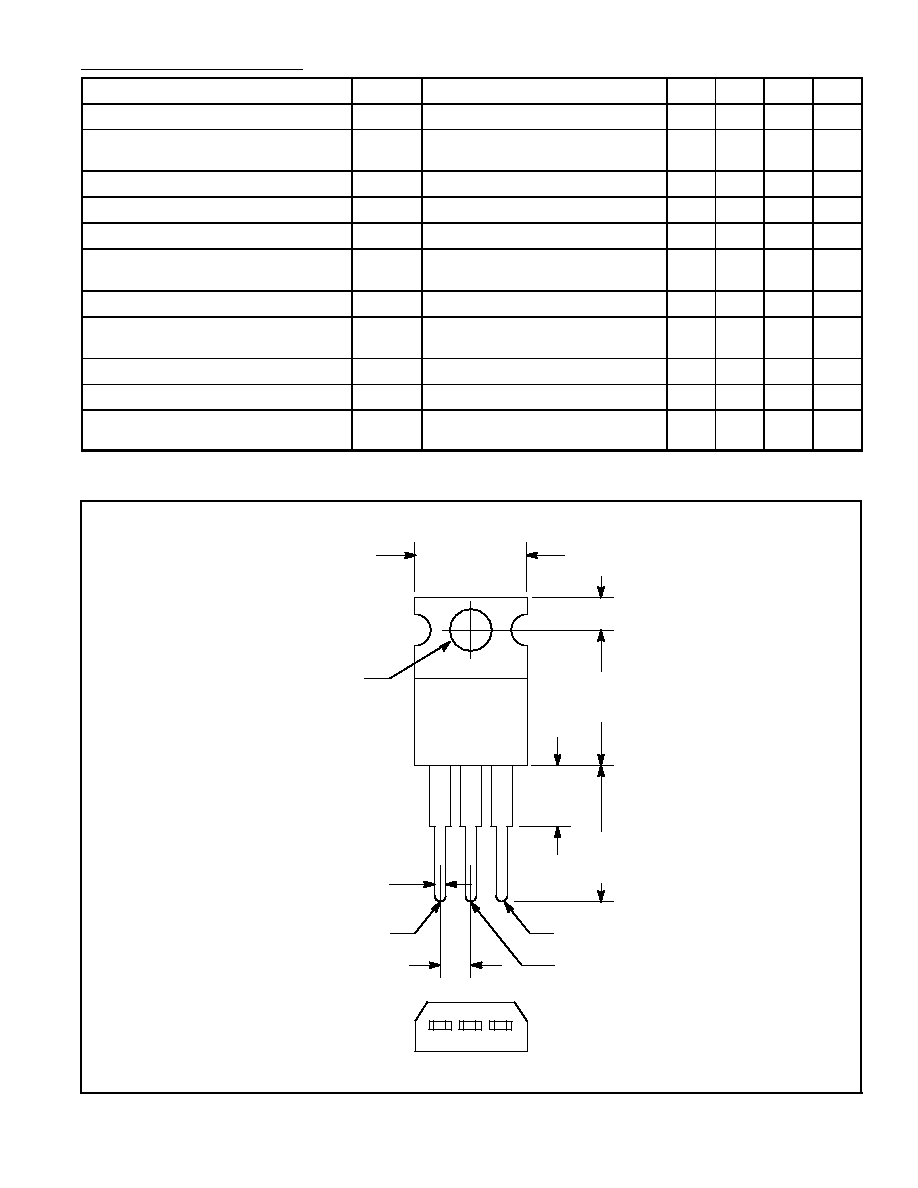
.250
(6.35)
Max
.500
(12.7)
Max
.500
(12.7)
Min
.110 (2.79)
.420 (10.67)
Max
.070 (1.78) Max
Cathode
.100 (2.54)
Anode/Tab
Gate
.147 (3.75)
Dia Max