 | –≠–ª–µ–∫—Ç—Ä–æ–Ω–Ω—ã–π –∫–æ–º–ø–æ–Ω–µ–Ω—Ç: NTE5705 | –°–∫–∞—á–∞—Ç—å:  PDF PDF  ZIP ZIP |

NTE5700 thru NTE5705
Industrial Power Module
Description:
The NTE5700 through NTE5705 series of Integrated Power Circuits consist of power thyristors and
power diodes configured in a single package. Applications include power supplies, control circuits
and battery chargers.
Features:
D
Glass Passivated Junctions for Greater Reliability
D
Electrically Isolated Base Plate
D
High Dynamic Characteristics
Absolute Maximum Ratings:
Maximum Repetitive Peak Reverse Voltage (V
S
£ 0), V
RRM
1200V
. . . . . . . . . . . . . . . . . . . . . . . . . . . .
Maximum Non--Repetitive Peak Reverse Voltage, V
RSM
1300V
. . . . . . . . . . . . . . . . . . . . . . . . . . . . . . .
Maximum Repetitive Peak Off State Voltage Gate Open Circuit, V
DRM
1200V
. . . . . . . . . . . . . . . . . .
Thermal and Mechanical Characteristics:
Junction Operating Temperature Range, T
J
--40∞ to +125∞C
. . . . . . . . . . . . . . . . . . . . . . . . . . . . . . . . . .
Storage Temperature Range, T
stg
--40∞ to +150∞C
. . . . . . . . . . . . . . . . . . . . . . . . . . . . . . . . . . . . . . . . . .
Maximum Internal Thermal Resistance, One Junction to Case, R
thJC
DC Operation
2.24K/W
. . . . . . . . . . . . . . . . . . . . . . . . . . . . . . . . . . . . . . . . . . . . . . . . . . . . . . . . . . . .
Maximum Thermal Resistance, Base to Heatsink, R
thCS
Mounting Surface Smooth and Greased
0.10K/W
. . . . . . . . . . . . . . . . . . . . . . . . . . . . . . . . . . . . .
Mounting Torque, Base to Heatsink ±10% (Note 1), T
5Nm
. . . . . . . . . . . . . . . . . . . . . . . . . . . . . . . . . .
Approximate Weight, wt
58g (2.0oz)
. . . . . . . . . . . . . . . . . . . . . . . . . . . . . . . . . . . . . . . . . . . . . . . . . . . . . .
Note 1. A mounting compound is recommended and the torque should be checked after a period of
about 3 hours to allow for the spread of the compound.

Electrical Characteristics:
Parameter
Symbol
Test Conditions
Rating Unit
Forward Conduction
Maximum DC Output Current
I
O
T
C
= +85∞C, Full Bridge Circuits
(NTE5700, NTE5701, NTE5702)
25
A
Maximum Average On--State
and Forward Current
I
T(AV)
I
F(AV)
180∞ Sine Wave Conduction Circuits
(All Types)
12.5
A
Maximum RMS Current
I
RMS
180∞ Sine Wave Conduction Circuit
(NTE5702)
28
A
Maximum Peak, One--Cycle
N
R
titi
O St t
I
TSM
10ms
100% V
RRM
R
li d
Sinusoidal Half Wave,
I iti l T
T M
300
A
Non--Repetitive On--State
or Forward Current
or
I
FSM
8.3ms Reapplied
Initial T
J
= T
J
Max
315
A
or Forward Current
I
FSM
10ms
No Voltage
R
li d
357
A
8.3ms Reapplied
375
A
Maximum I
2
t for Fusing
I
2
t
10ms
100% V
RRM
R
li d
Initial T
J
= T
J
Max
450
A
2
s
8.3ms Reapplied
410
A
2
s
10ms
No Voltage
R
li d
637
A
2
s
8.3ms Reapplied
580
A
2
s
Maximum I
2
÷t for Fusing
I
2
÷t
t = 0.1 to 10ms, No Voltage Reapplied, Note 2
6365 A
2
÷s
Maximum Value of Threshold
Voltage
V
T(TO)
T
J
= +125∞C
0.82
V
Maximum Value of On--State
Slope Resistance
r
T
T
J
= +125∞C
12
mW
Maximum Peak On--State
F
d V lt
V
TM
I
TM
= p x I
T(AV)
T
J
= +25∞C,
180∞ C diti
1.35
V
or Forward Voltage
V
FM
I
FM
= p x I
F(AV)
180∞ Condition
1.35
V
Maximum Non--Repetitive Rate
of Rise of Turned On Circuit
di/dt
T
J
= +125∞C, from 0.67V
DRM
, I
TM
= p x I
T(AV)
,
I
g
= 500mA, t
r
< 0.5ms, t
p
> 6ms
200
A/ms
Maximum Holding Current
I
H
T
J
= +25∞C, Anode Supply = 6V,
Resistive Load, Gate Open Circuit
100
mA
Maximum Latching Current
I
L
T
J
= +25∞C, Anode Supply = 6V,
Resistive Load
250
mA
Triggering
Maximum Peak Gate Power
P
GM
8.0
W
Maximum Average Gate Power
P
G(AV)
2.0
W
Maximum Peak Gate Current
I
GM
2.0
A
Maximum Peak Negative Gate
Voltage
--V
GM
10
V
Maximum Gate Voltage Required
t T i
V
GT
T
J
= --40∞C
Anode Supply = 6V
R i ti
L d
3.0
V
to Trigger
T
J
= +25∞C
Resistive Load
2.0
V
T
J
= +125∞C
1.0
V
Electrical Characteristics (Cont'd):
Parameter
Symbol
Test Conditions
Rating Unit
Triggering (Cont'd)
Maximum Gate Current Required
t T i
I
GT
T
J
= --40∞C
Anode Supply = 6V
R i ti
L d
90
mA
to Trigger
T
J
= +25∞C
Resistive Load
60
mA
T
J
= +125∞C
35
mA
Maximum Gate Voltage that will
not Trigger
V
GD
T
J
= +125∞C, Rated V
DRM
Applied
0.2
V
Blocking
Maximum Critical Rate of Rise of
Off--State Voltage
dv/
dt
T
J
= +125∞C, Exponential to 0.67V
DRM
,
Gate Open Circuit
200
V/ms
Maximum Peak Reverse and
Off--State Leakage Current
I
RM
T
J
= T
J
Max, Gate Open Circuit
10
mA
Off--State Leakage Current
at V
RRM
, V
DRM
I
DM
2.0
mA
RMS Isolation Voltage
V
INS
50Hz, Circuit to Base, All Terminals Shorted
2500
V
Note 2. I
2
t for time t
x
= I
2
÷t Ø ÷t
x
.
Pin Connection and Schematic Diagrams:
NTE No.
Description
Terminal Positions
Schematic Diagrams
5700
Single Phase,
Hybrid Bridge,
Common Cathode,
Freewheeling Diode
5701
Single Phase,
Hybrid Bridge,
Common Anode,
Freewheeling Diode
5702
Single Phase,
All SCR Bridge
* For transient protection, a Metal Oxide Varistor (MOV) may be connected externally across terminals AC1 & AC2.
AC1
AC2
G1
G2
(--)
(+)
AC1
AC2
*
G1
G2
(--)
(+)
AC1
AC2
G1
G2
(--)
(+)
AC1
AC2
*
G1
G2
(--)
(+)
AC2
AC1
G2
G3
(--)
(+)
G1
G4
AC1
AC2
*
G1
G3
G2
G4
(--)
(+)

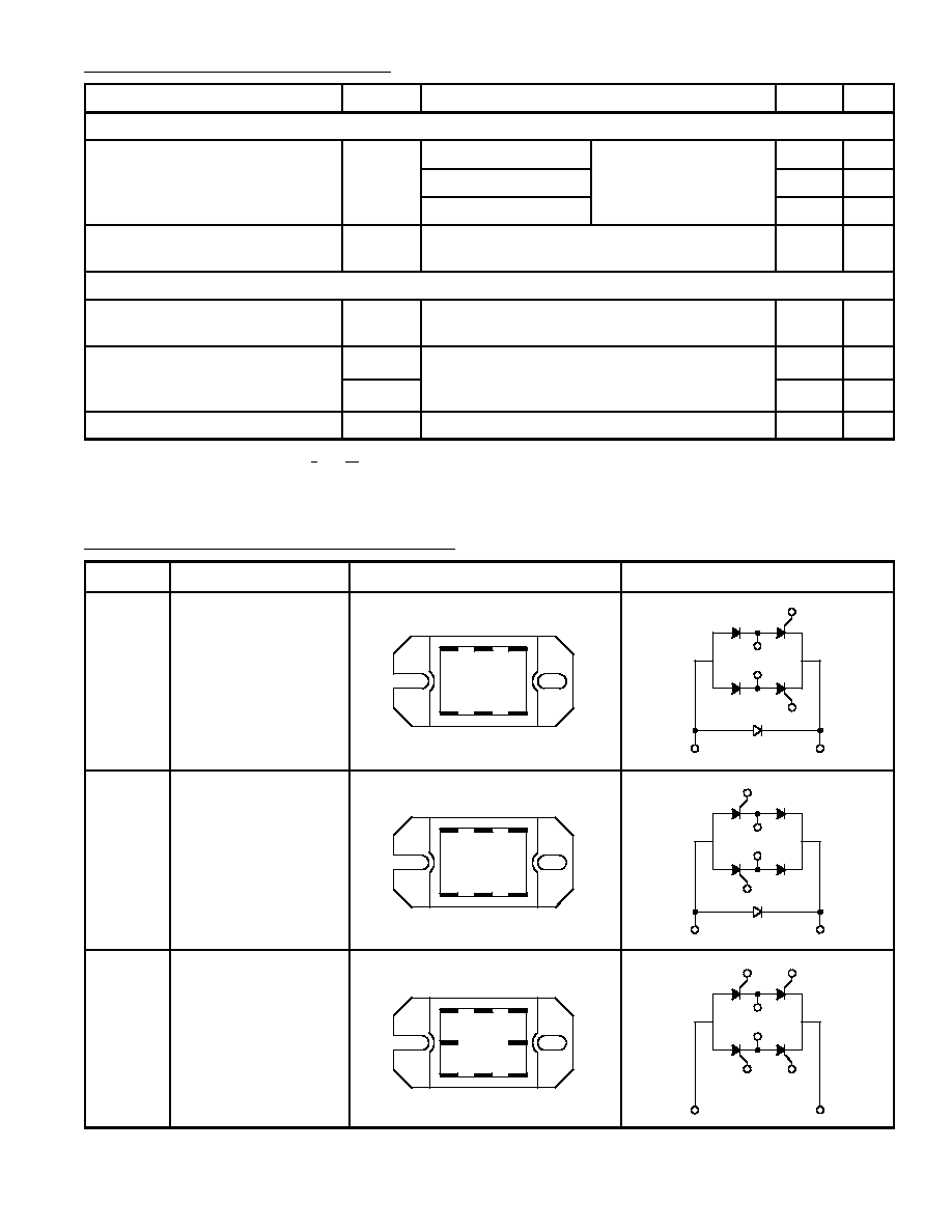
Pin Connection and Schematic Diagrams (Cont'd):
NTE No.
Description
Terminal Positions
Schematic Diagrams
5703
SCR AC Switch
5704
Hybrid Doubler
5705
SCR Doubler
* For transient protection, a Metal Oxide Varistor (MOV) may be connected externally across terminals AC1 & AC2.
1.910 (48.5)
.200
(5.08)
1.250
(31.75)
2.500 (63.5)
.980
(24.89)
Max
.600 (15.24)
Max
.500 (12.7)
NOTE: Can be used with Heat Sink NTE441A
AC1
G2
G1
AC2
*
G2
G1
AC1
AC2
AC1
G1
(--)
(+)
G1
AC1
(--)
(+)
AC
G1
G2
(--)
(+)
G2
AC1
(--)
(+)
G1