 | –≠–ª–µ–∫—Ç—Ä–æ–Ω–Ω—ã–π –∫–æ–º–ø–æ–Ω–µ–Ω—Ç: NTE65101 | –°–∫–∞—á–∞—Ç—å:  PDF PDF  ZIP ZIP |
NTE65101
Integrated Circuit
256 x 4≠Bit Static Random Access Memory (SRAM)
Description:
The NTE65101 is a CMOS 1024≠bit device organized in 256 words by 4 bits in a 22≠Lead DIP type
package. This device offers ultra low power and fully static operation with a single 5V supply. Sepa-
rate data inputs and data outputs permit maximum flexibility in bus≠oriented systems. Data retention
at a power supply as low as 2V over temperature readily allows design into applications using battery
backup for nonvolatility. The NTE65101 is fully static and does not require clocking in standby mode.
Features:
D
Organized as 256 Bytes of 4≠Bits
D
Static Operation
D
Low Standby Power
D
Three≠State Output
D
Single 5V Power Supply
D
Data Retention to 2V
D
TTL Compatible
D
Maximum Access Time: 450ns
Absolute Maximum Ratings: (Voltages referenced to V
SS
Pin8)
Supply Voltage, V
CC
≠0.5 to +7V
. . . . . . . . . . . . . . . . . . . . . . . . . . . . . . . . . . . . . . . . . . . . . . . . . . . . . . . . .
Input Voltage, V
in
≠0.3 to V
CC
+0.3V
. . . . . . . . . . . . . . . . . . . . . . . . . . . . . . . . . . . . . . . . . . . . . . . . . . . . . .
Operating Temperature Range, T
A
≠40
∞
to +85
∞
C
. . . . . . . . . . . . . . . . . . . . . . . . . . . . . . . . . . . . . . . . . . .
Storage Temperature Range, T
stg
≠65
∞
to +150
∞
C
. . . . . . . . . . . . . . . . . . . . . . . . . . . . . . . . . . . . . . . . . .
Note 1. This device contains circuitry to protect the inputs against damage due to high static voltages
or electric fields; however, it is advised that normal precautions be taken to avoid application
of any voltage higher than maximum rated voltages to this high impedance circuit.
DC Electrical Characteristics: (V
CC
= 5V
±
5%, T
A
= 0
∞
to +70
∞
C unless otherwise specified)
Parameter
Symbol
Test Conditions
Min
Typ
Max
Unit
Input Current
I
in
Note 3
≠
5.0
≠
nA
Input High Voltage
V
IH
2.2
≠
V
CC
V
Input Low Voltage
V
IL
≠0.3
≠
0.65
V
Output High Voltage
V
OH
I
OH
= ≠1mA
2.4
≠
≠
V
Output Low Voltage
V
OL
I
OL
= 2mA
≠
≠
0.4
V
Output Leakage Current
I
LO
CE1 = 2.2V, V
OL
= 0V to V
CC
, Note 3
≠
≠
±
1.0
µ
A
Operating Current
I
CC1
V
in
= V
CC
, except CE1
0.65V,
Outputs open
≠
9.0
22
mA
I
CC2
V
in
= 2.2V, except CE1
0.65V,
Outputs open
≠
13
27
mA
Standby Current
I
CCL
CE2
0.2V, Note 3, Note 4
≠
≠
10
µ
A
Note 2. Typical values are T
A
= +25
∞
C and nominal voltage.
Note 3. Current through all inputs and outputs included in I
CCL
measurement.
Note 4. Low current state is for CE2 = 0 only.
Capacitance:
Parameter
Symbol
Test Conditions
Min
Typ
Max
Unit
Input Capacitance
C
in
V
in
= 0V
≠
4.0
8.0
pF
Output Capacitance
C
out
V
out
= 0V
≠
8.0
12.0
pF
Note 2. Typical values are T
A
= +25
∞
C and nominal voltage.
Low V
CC
Retention Characteristics: (T
A
= 0
∞
to +70
∞
C unless otherwise specified)
Parameter
Symbol
Test Conditions
Min
Typ
Max
Unit
V
CC
for Data Retention
V
DR
2.0
≠
≠
V
Data Retention Current
I
CCDR1
CE2
0.2V, V
DR
= 2V
≠
0.14
10
µ
A
Chip Deselect to Data Retention Time
t
CDR
0
≠
≠
ns
Operation Recovery Time
t
R
Note 5
t
RC
≠
≠
ns
Note 2. Typical values are T
A
= +25
∞
C and nominal voltage.
Note 5. t
RC
= Read Cycle Time.
AC Operating Conditions and Characteristics: (Full operating voltage and temperature unless
otherwise specified)
AC Test Conditions:
Condition
Value
Input Pulse Levels
+0.65V to 2.2V
Input Rise and Fall Times
20ns
Output Load ≠
1 TTL Gate and C
L
= 100pF
Timing Measurement Reference Level
1.5V

AC Operating Conditions and Characteristics (Cont'd): (Full operating voltage and temperature
unless otherwise specified)
Read Cycle:
Parameter
Symbol
Min
Max Unit
Read Cycle Time
t
RC
450
≠
ns
Access Time
t
A
≠
450
ns
Read Cycle (Cont'd):
Parameter
Symbol
Min
Max
Unit
Address Setup Time
t
AS
20
≠
ns
Address Hold Time
t
AH
0
≠
ns
Chip Enable (CE1) to Output
t
CO1
≠
400
ns
Chip Enable (CE2) to Output
t
CO2
≠
500
ns
Output Disable to Output
t
OD
≠
250
ns
Data Output to High Z State
t
DF
0
130
ns
Previous Read Data Valid with Respect to Address Change
t
OH1
0
≠
ns
Previous Read Data Valid with Respect to Chip Enable
t
OH2
0
≠
ns
Write Cycle:
Parameter
Symbol
Min
Max
Unit
Write Cycle
t
WC
450
≠
ns
Write Delay
t
AW
130
≠
ns
Chip Enable (CE1) to Write
t
CW1
350
≠
ns
Chip Enable (CE2) to Write
t
CW2
350
≠
ns
Data Setup
t
DW
250
≠
ns
Data Hold
t
DH
50
≠
ns
Write Pulse
t
WP
250
≠
ns
Write Recovery
t
WR
50
≠
ns
Output Disable Setup
t
DS
130
≠
ns
Truth Table:
CE1
CE2
OD
R/W
D
in
Output
Mode
H
X
X
X
X
High Z
Not Selected
X
L
X
X
X
High Z
Not Selected
X
X
H
H
X
High Z
Output Disable
L
H
H
L
X
High Z
Write
L
H
L
L
X
D
in
Write
L
H
L
H
X
D
out
Read
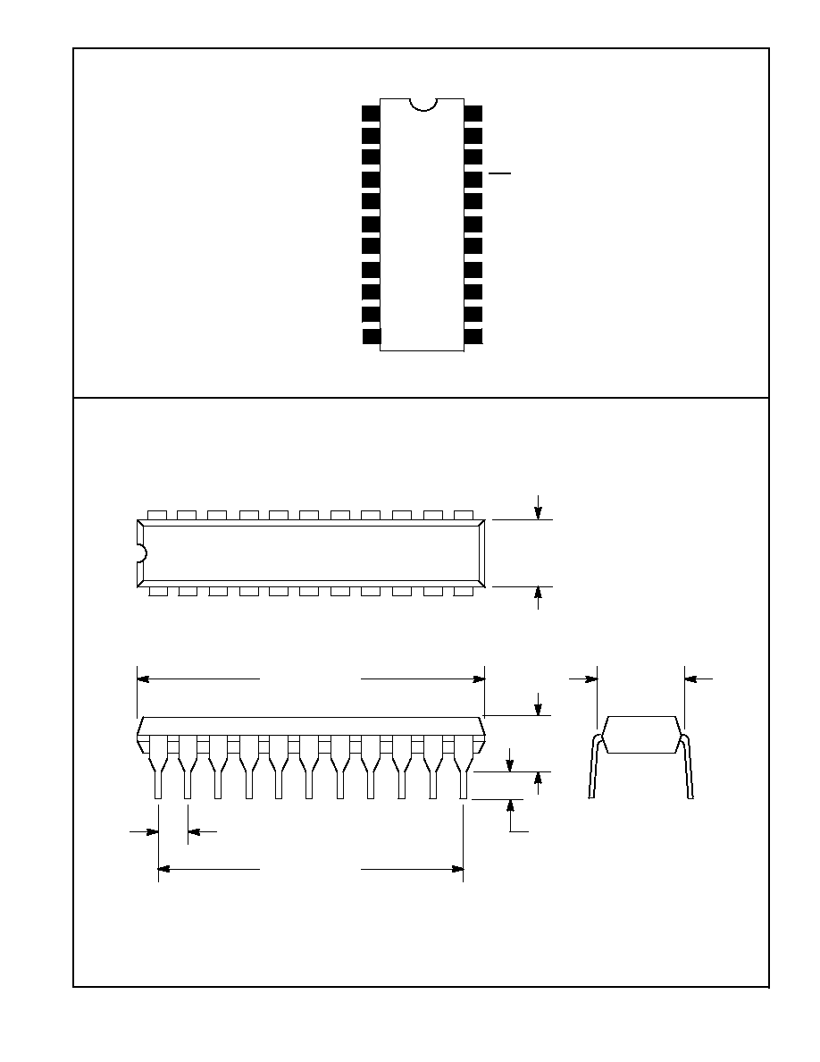
CE 1
V
CC
Pin Connection Diagram
DO 3
R/W
GND
A5
A0
A1
A6
OD
DI 4
A7
A2
1
2
3
4
A3
5
6
7
22
21
20
19
A4
18
17
CD 2
16
8
15
DO 1
9
14
DI 1
DI 3
10
13
DI 2
11
12
DO 2
DO 4
22
12
1
11
1.300 (33.0)
1.000 (25.4)
.100 (2.54)
.410
(11.41)
.216
(5.5)
.110 (2.79)
.400
(10.16)