 | –≠–ª–µ–∫—Ç—Ä–æ–Ω–Ω—ã–π –∫–æ–º–ø–æ–Ω–µ–Ω—Ç: NTE7001 | –°–∫–∞—á–∞—Ç—å:  PDF PDF  ZIP ZIP |
NTE7001
Integrated Circuit
Horizontal Combination Circuit for
Color TV & Computer Monitors
Description:
The NTE7001 is a monolithic integrated circuit in a 16≠Lead DIP type package intended for use in
color television receivers.
Features:
D
Horizontal Oscillation Based on the Threshold Switching Principle
D
Phase Comparasion Between Sync Pulse and Oscillator Voltage (
1
)
D
Internal Key Pulse for Phase Detector (
1
) (Additional Noise Limiting)
D
Phase Comparison Between Line Flyback Pulse and Oscillator Volatge (
2
)
D
Larger Catching Range Obtained by Coincidence Detector (
3
; Between Sync and Key Pulse)
D
Switch for Changing the Filter Characteristic and the Gtae Circuit (VCR Operation)
D
Sync Separator
D
Noise Separator
D
Vertical Sync Separator and Output Stage
D
Color Burst Keying and Line Flyback Blanking Pulse Generator
D
Phase Shifter for the Output Pulse
D
Output Pulse Duration Switching
D
Output Stage with Separate Supply Voltage for Direct Drive of Thyristor Deflection Circuits
D
Low Supply Voltage Protection
Applications:
D
Video Monitors
D
TV Receivers
Absolute Maximum Ratings:
Supply Voltage
at Pin1 (Voltage Source), V
1≠16
13.2V
. . . . . . . . . . . . . . . . . . . . . . . . . . . . . . . . . . . . . . . . . . . . . .
at Pin2, V
2≠16
18V
. . . . . . . . . . . . . . . . . . . . . . . . . . . . . . . . . . . . . . . . . . . . . . . . . . . . . . . . . . . . . . . .
Voltages
Pin4, V
4≠16
13.2V
. . . . . . . . . . . . . . . . . . . . . . . . . . . . . . . . . . . . . . . . . . . . . . . . . . . . . . . . . . . . . . . .
Pin9,
±
V
9≠16
6V
. . . . . . . . . . . . . . . . . . . . . . . . . . . . . . . . . . . . . . . . . . . . . . . . . . . . . . . . . . . . . . . . . .
Pin10,
±
V
10≠16
6V
. . . . . . . . . . . . . . . . . . . . . . . . . . . . . . . . . . . . . . . . . . . . . . . . . . . . . . . . . . . . . . . .
Pin11, V
11≠16
13.2V
. . . . . . . . . . . . . . . . . . . . . . . . . . . . . . . . . . . . . . . . . . . . . . . . . . . . . . . . . . . . . .

Absolute Maximum Ratings (Cont'd):
Currents
Pin2 and Pin3 (Thyristor Driving, Peak Value), I
2M
, ≠I
3M
650mA
. . . . . . . . . . . . . . . . . . . . . . . .
Pin2 and Pin3 (Transistor Driving, Peak Value), I
2M
, ≠I
3M
400mA
. . . . . . . . . . . . . . . . . . . . . . .
Pin4, I
4
1mA
. . . . . . . . . . . . . . . . . . . . . . . . . . . . . . . . . . . . . . . . . . . . . . . . . . . . . . . . . . . . . . . . . . . .
Pin6,
±
I
6
10mA
. . . . . . . . . . . . . . . . . . . . . . . . . . . . . . . . . . . . . . . . . . . . . . . . . . . . . . . . . . . . . . . . . .
Pin7, ≠I
7
10mA
. . . . . . . . . . . . . . . . . . . . . . . . . . . . . . . . . . . . . . . . . . . . . . . . . . . . . . . . . . . . . . . . . .
Pin11, I
11
2mA
. . . . . . . . . . . . . . . . . . . . . . . . . . . . . . . . . . . . . . . . . . . . . . . . . . . . . . . . . . . . . . . . . . .
Total Power Dissipation, P
TOT
800mW
. . . . . . . . . . . . . . . . . . . . . . . . . . . . . . . . . . . . . . . . . . . . . . . . . . . .
Operating Ambient Temperature Range, T
A
≠20
∞
to +70
∞
C
. . . . . . . . . . . . . . . . . . . . . . . . . . . . . . . . . . .
Storage Temperature Range, T
stg
≠25
∞
C to +125
∞
C
. . . . . . . . . . . . . . . . . . . . . . . . . . . . . . . . . . . . . . . .
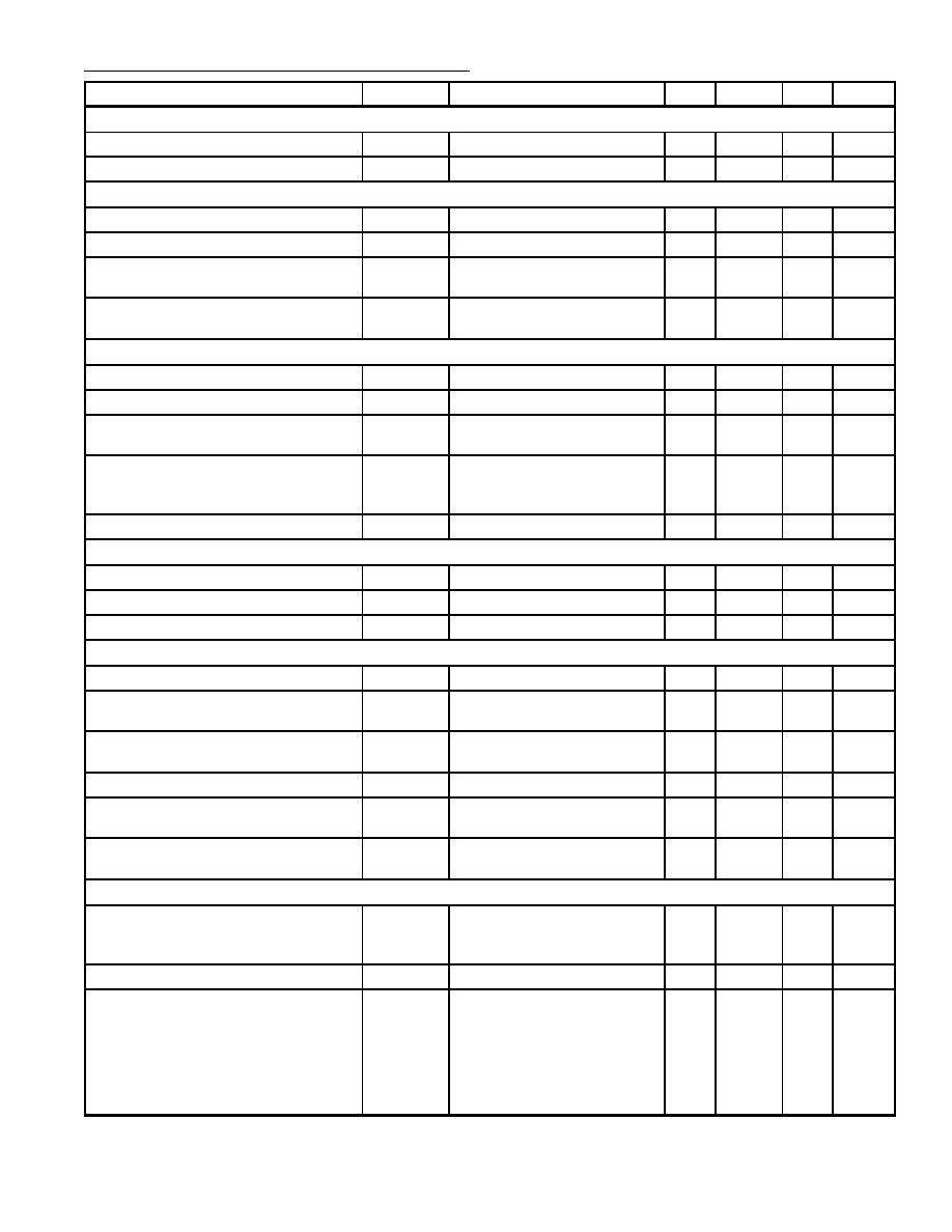
DC and AC Electrical Characteristics: (V
CC
= 12V, T
A
= +25
∞
C unless otherwise specified)
Parameter
Symbol
Test Conditions
Min
Typ
Max
Unit
Sync Separator
Input Switch Voltage
V
9≠16
≠
0.8
≠
V
Input Keying Current
I
9
5
≠
100
µ
A
Input Leakage Current
I
9
V
9≠16
= ≠5V
≠
≠
1
µ
A
Input Switching Current
I
9
≠
≠
5
µ
A
Switch OFF Current
I
9
100
150
≠
µ
A
Input Signal (Peak≠to≠Peak Value)
V
9≠16(P≠P)
Note 1
3
≠
4
V
Noise Separator
Input Switching Voltage
V
10≠16
≠
1.4
≠
V
Input Keying Current
I
10
5
≠
100
µ
A
Input Switching Current
I
10
100
150
≠
µ
A
Input Leakage Current
I
10
V
10≠16
= ≠5V
≠
≠
1
µ
A
Input Signal (Peak≠to≠Peak Value)
V
10≠16(P≠P)
Note 1
3
≠
4
V
Permissible Superimposed Noise Signal
(Peak≠to≠Peak Value)
V
10≠16(P≠P)
≠
≠
7
V
Line Flyback Pulse
Input Current
I
6
0.02
1
2
mA
Input Switching Voltage
V
6≠16
≠
1.4
≠
V
Input Limiting Voltage
V
6≠16
≠0.7
≠
+1.4
V
Switching on VCR
Input Voltage
V
11≠16
0 to 2.5
V
9 to V
1≠16
V
Input Current
≠I
11
≠
≠
200
µ
A
I
11
≠
≠
2
mA
Pulse Duration Switch [t = 7
µ
s (Thyristor Driving)]
Input Voltage
V
4≠16
≠
9.4 to V
1≠16
V
Input Current
I
4
200
≠
≠
µ
A
Pulse Duration Switch [t = 14
µ
s + t
D
(Transistor Driving)]
Input Voltage
V
4≠16
0
≠
3.5
V
Input Current
≠I
4
200
≠
≠
µ
A
Note 1. Permissible Range 1V to 7V.
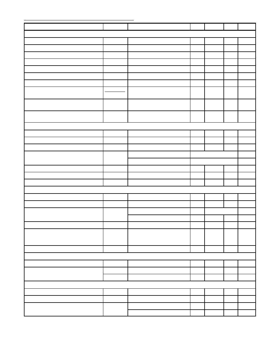
DC and AC Electrical Characteristics (Cont'd): (V
CC
= 12V, T
A
= +25
∞
C unless otherwise specified)
Parameter
Symbol
Test Conditions
Min
Typ
Max
Unit
Pulse Duration Switch (t = 0, V
3≠16
= 0 or Input Pin4 Open)
Input Voltage
V
4≠16
5.4
≠
6.6
V
Input Current
I
4
≠
0
0
µ
A
Vertical Sync Pulse (Positive≠Going)
Output Voltage (Peak≠to≠Peak Value)
V
8≠16(P≠P)
10
11
≠
V
Output Resistance
R
8
≠
2
≠
k
Delay Between Leading Edge of Input
and Output Signal
t
ON
≠
15
≠
µ
s
Delay Between Trailing Edge of Input
and Output Signal
t
OFF
≠
t
ON
≠
µ
s
Burst Gating Pulse (Positive≠Going)
Output Voltage (Peak≠to≠Peak Value)
V
7≠16(P≠P)
10
11
≠
V
Output Resistance
R
7
≠
70
≠
Pulse Duration
t
p
V
7≠16
= 7V
≠
3.7
4.0
4.3
≠
≠
µ
s
µ
s
Phase Relation Between Middle of Sync
Pulse at the Input and the Leading
Edge of the Burst Gating Pulse
t
V
7≠16
= 7V
2.15
2.65
3.15
µ
s
Output Trailing Edge Current
I
7
≠
2
≠
mA
Line Flyback≠Blanking Pulse (Positive≠Going)
Output Voltage (Peak≠to≠Peak Value)
V
7≠16(P≠P)
4
5
≠
V
Output Resistance
R
7
≠
70
≠
Output Trailing Edge Current
I
7
≠
2
≠
mA
Line Drive Pulse (Positive≠Going)
Output Voltage (Peak≠to≠Peak Value)
V
3≠16(P≠P)
≠
10.5
≠
V
Output Resistance for Leading Edge of
Line Pulse
R
3
≠
2.5
≠
Output Resistance for Trailing Edge of
Line Pulse
R
3
≠
20
≠
Pulse Duration (Thyristor Driving)
t
p
V
4≠16
= 9.4 to V
1≠16
V
5.5
7.0
8.5
µ
s
Pulse Duration (Transistor Driving)
t
p
V
4≠16
= 0 to 4V, t
FP
= 12
µ
s,
Note 2
≠
14 + t
D
≠
µ
s
Supply Voltage for Switching OFF the
Output Pulse
V
1≠16
≠
4
≠
V
Overall Phase Relation
Phase Relation Between Middle of Sync
Pulse and the Middle of the Flyback
Pulse
t
Note 3
≠
2.6
≠
µ
s
Tolerance of Phase Relation
|
t|
≠
≠
0.7
µ
s
The Adjustment of the Overall Phase
Relation and Consequently the
Leading Edge of the Line Drive Oc-
curs Automatically by Phase Con-
trol
2
. If Additional Adjustment is
Applied it can be Arranged by Cur-
rent Supply at Pin5.
I
5
/
t
≠
30
≠
µ
A/
µ
s
Note 2. t
D
= Switch≠OFF Delay of Line Output Stage.
Note 3. Line Flyback Pulse Duration t
FP
= 12
µ
s.
DC and AC Electrical Characteristics (Cont'd): (V
CC
= 12V, T
A
= +25
∞
C unless otherwise specified)
Parameter
Symbol
Test Conditions
Min
Typ
Max
Unit
Oscillator
Threshold Voltage Low Level
V
14≠16
≠
4.4
≠
V
Threshold Voltage High Level
V
14≠16
≠
7.6
≠
V
Discharge Current
±
I
14
≠
0.47
≠
mA
Frequency; Free Running
f
O
C
OSC
= 4.7nF, R
OSC
= 12k
≠
15.625
≠
kHz
Spread of Frequency
f
O
/f
O
Note 4
≠
<
±
5
≠
%
Frequency Control Sensitivity
f
O
/
I
15
≠
31
≠
Hz/
µ
A
Adjustment Range of Network in Circuit
f
O
/f
O
≠
±
10
≠
%
Influence of Supply Voltage on Fre-
quency
f
O
/f
O
V/V
NOM
Note 4
≠
<
±
0.05
≠
%
Change of Frequency when V
1≠16
Drops to 5V
f
O
Note 4
≠
<
±
10
≠
%
Temperature Coefficient of Oscillator
Frequency
Note 4
≠
<
±
10
≠4
≠
Hz/
∞
C
Phase Comparison
1
Control Voltage Range
V
13≠16
3.8
8.2
≠
V
Control Current (Peak Value)
±
I
13M
1.9
2.3
≠
mA
Output Leakage Current
I
13
V
13≠16
= 4 to 8V
≠
≠
1
µ
A
Output Resistance
R
13
V
13≠16
= 4 to 8V, Note 5
High Ohmic
V
13≠16
< 3.8V or > 8.2V, Note 6
Low Ohmic
Control Sensitivity
≠
2
≠
kHz/
µ
s
Catching and Holding Range
f
82k
Between Pins 13 and 15
≠
±
780
≠
Hz
Spread of Catching and Holding Range
(
f)
Note 4
≠
±
10
≠
%
Phase Comparison
2
and Phase Shifter
Control Voltage range
V
5≠16
5.4
≠
7.6
V
Control Current (Peak Value)
±
I
5M
≠
1
≠
mA
Output Resistance
R
5
V
5≠16
= 5.4 to 7.6V, Note 7
≠
High Ohmic
V
5≠16
< 5.4 or > 7.6V
≠
8
≠
k
Input Leakage Current
I
5
V
5≠16
= 5.4 to 7.6V
≠
≠
5
µ
A
Permissible Delay Between Leading
Edge of Output Pulse and Leading
Edge of Flyback Pulse
t
D
t
FP
= 12
µ
s
≠
≠
15
µ
s
Static Control Error
t/
t
D
≠
≠
0.2
%
Coincidence Detector
3
Output Voltage
V
11≠16
0.5
0
6.0
V
Output Current (Peak Value)
I
11M
Without Coincidence
≠
0.1
≠
mA
≠I
11M
With Coincidence
≠
0.5
≠
mA
Time Constant Switch
Output Voltage
V
12≠16
≠
6
≠
V
Output Current (Limited)
±
I
12
≠
≠
1
mA
Output Resistance
R
12
V
11≠16
= 2.5 to 7V
≠
0.1
≠
k
V
11≠16
< 1.5V or > 9V
≠
60
≠
k
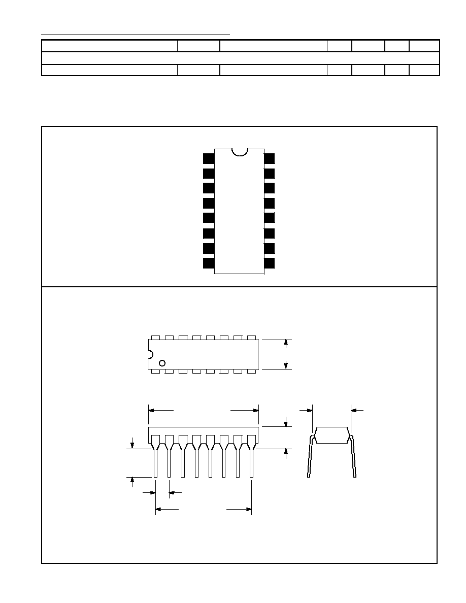
DC and AC Electrical Characteristics (Cont'd): (V
CC
= 12V, T
A
= +25
∞
C unless otherwise specified)
Parameter
Symbol
Test Conditions
Min
Typ
Max
Unit
Internal Gating Pulse
Pulse Duration
t
p
≠
7.5
≠
µ
s
Note 4. Excluding External Component Tolerances.
Note 5. Current Source.
Note 6. Emitter≠Follower.
Note 7. Current Source.
Pin Connection Diagram
V
CC
1
2
3
4
Trigger Pulse Input
Line Pulse Output
Pulse Duration Switch
5
Phase Shifter
6
FB Pulse Input
7
Blank Pulse Output
16
15
14
13
GND
OSC Frequency Adjust
OSC Cap Input
Phase Detector 1
12
Time Constant Switch
11
VCR Switch/
10
Noise Separator
8
Vertical Sync Pulse Output
9
Video Input
Coincidence Detector
.260 (6.6) Max
16
9
1
8
.785 (19.9)
Max
.200 (5.08)
Max
.245
(6.22)
Min
.300
(7.62)
.700 (17.7)
.100 (2.54)