NTE7108
Integrated Circuit
1.3GHz Phase Locked Loop
w
/I
2
C Bus
Description:
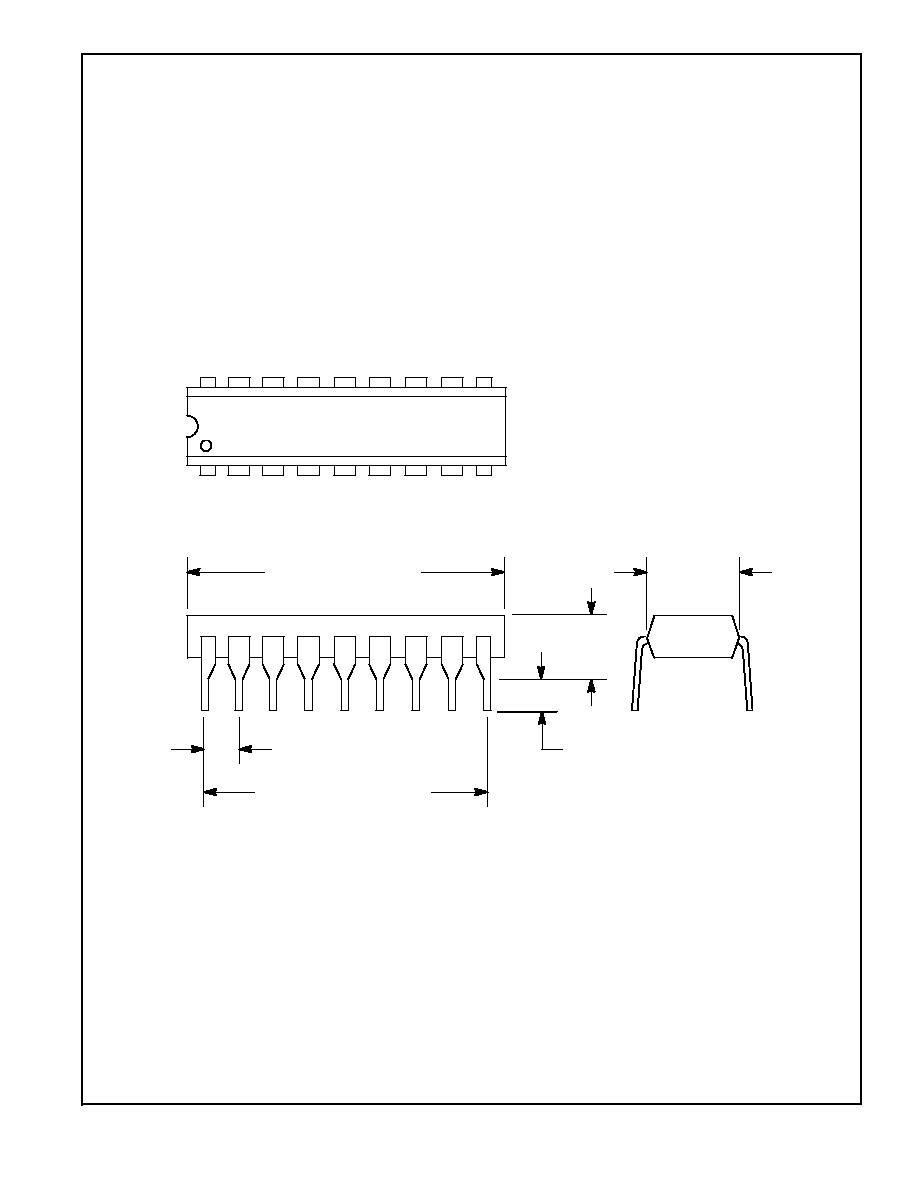
The NTE7108 is an integrated circuit in an 18≠Lead DIP type package and when used in combination
with a VCO (tuner), comprises a digital programmable phase≠locked loop (PLL) for television devices
designed to use the PLL frequency synthesis tuning principle.
The PLL provides a crystal≠stable frequency for tuner oscillators between 16
1300MHz in the
62.5kHz raster. By including an external prescaler 1/2, the component can also be used for synthesiz-
ing applications of up to 2.4GHz (e.g. satellite receivers). As a result, the resolution is doubled to
125kHz. The tuning process is controlled via an I
2
C bus by the microprocessor.
Features:
D
Low Current Consumption
D
Message Transmission Via I
2
C Bus
D
4 Software≠Controlled Outputs
D
Cost≠Effective and Space≠Saving Design
D
Prescaler Output Frequency is Free from Interference Radiation
Absolute Maximum Ratings: (Note 1)
Supply Voltage, V
S
≠0.3V to 6V
. . . . . . . . . . . . . . . . . . . . . . . . . . . . . . . . . . . . . . . . . . . . . . . . . . . . . . . . . .
Output PD, V
1
≠0.3V to V
S
. . . . . . . . . . . . . . . . . . . . . . . . . . . . . . . . . . . . . . . . . . . . . . . . . . . . . . . . . . . . . .
Crystal Q1, V
2
≠0.3V to V
S
. . . . . . . . . . . . . . . . . . . . . . . . . . . . . . . . . . . . . . . . . . . . . . . . . . . . . . . . . . . . . .
Crystal Q2, V
3
≠0.3V to V
S
. . . . . . . . . . . . . . . . . . . . . . . . . . . . . . . . . . . . . . . . . . . . . . . . . . . . . . . . . . . . . .
Bus Input/Output SDA, V
4
≠0.3V to V
S
. . . . . . . . . . . . . . . . . . . . . . . . . . . . . . . . . . . . . . . . . . . . . . . . . . . .
Bus Input SCL, V
5
≠0.3V to V
S
. . . . . . . . . . . . . . . . . . . . . . . . . . . . . . . . . . . . . . . . . . . . . . . . . . . . . . . . . . .
Port Output P7, V
6
≠0.3V to +16V
. . . . . . . . . . . . . . . . . . . . . . . . . . . . . . . . . . . . . . . . . . . . . . . . . . . . . . . .
Port Output P6, V
7
≠0.3V to +16V
. . . . . . . . . . . . . . . . . . . . . . . . . . . . . . . . . . . . . . . . . . . . . . . . . . . . . . . .
Port Output P5, V
8
≠0.3V to +16V
. . . . . . . . . . . . . . . . . . . . . . . . . . . . . . . . . . . . . . . . . . . . . . . . . . . . . . . .
Port Output P4, V
9
≠0.3V to +16V
. . . . . . . . . . . . . . . . . . . . . . . . . . . . . . . . . . . . . . . . . . . . . . . . . . . . . . . .
Port Output P3, V
10
≠0.3V to +16V
. . . . . . . . . . . . . . . . . . . . . . . . . . . . . . . . . . . . . . . . . . . . . . . . . . . . . . . .
Port Output P2, V
11
≠0.3V to +16V
. . . . . . . . . . . . . . . . . . . . . . . . . . . . . . . . . . . . . . . . . . . . . . . . . . . . . . . .
Port Output P1, V
12
≠0.3V to +16V
. . . . . . . . . . . . . . . . . . . . . . . . . . . . . . . . . . . . . . . . . . . . . . . . . . . . . . . .
Port Output P0, V
13
≠0.3V to +16V
. . . . . . . . . . . . . . . . . . . . . . . . . . . . . . . . . . . . . . . . . . . . . . . . . . . . . . . .
Signal Input UHF/VHF, V
15
≠0.3V to +2.5V
. . . . . . . . . . . . . . . . . . . . . . . . . . . . . . . . . . . . . . . . . . . . . . . .
Reference Input REF, V
16
≠0.3V to +2.5V
. . . . . . . . . . . . . . . . . . . . . . . . . . . . . . . . . . . . . . . . . . . . . . . . .
Output Active Filter V
D
, V
18
≠0.3V to V
S
. . . . . . . . . . . . . . . . . . . . . . . . . . . . . . . . . . . . . . . . . . . . . . . . . . .
Bus Output SDA (Open Collector), I
4L
≠1mA to +5mA
. . . . . . . . . . . . . . . . . . . . . . . . . . . . . . . . . . . . . . .
Port Output P7 (Open Collector), I
6L
≠1mA to +5mA
. . . . . . . . . . . . . . . . . . . . . . . . . . . . . . . . . . . . . . . .
Note 1. Stresses above those listed under "Absolute Maximum Ratings" may cause permanent damage
to the device. Exposure to absolute maximum rating conditions for extended periods may affect
device reliability.

Absolute Maximum Ratings (Cont'd): (Note 1)
Port Output P6 (Open Collector), I
7L
≠1mA to +5mA
. . . . . . . . . . . . . . . . . . . . . . . . . . . . . . . . . . . . . . . .
Port Output P5 (Open Collector), I
8L
≠1mA to +5mA
. . . . . . . . . . . . . . . . . . . . . . . . . . . . . . . . . . . . . . . .
Port Output P4 (Open Collector), I
9L
≠1mA to +5mA
. . . . . . . . . . . . . . . . . . . . . . . . . . . . . . . . . . . . . . . .
Junction Temperature, T
J
+125
∞
C
. . . . . . . . . . . . . . . . . . . . . . . . . . . . . . . . . . . . . . . . . . . . . . . . . . . . . . . . .
Storage Temperature range, T
stg
≠40
∞
C to +125
∞
C
. . . . . . . . . . . . . . . . . . . . . . . . . . . . . . . . . . . . . . . . .
Thermal Resistance, System to Ambient, R
SA
80K/W
. . . . . . . . . . . . . . . . . . . . . . . . . . . . . . . . . . . . .
Note 1. Stresses above those listed under "Absolute Maximum Ratings" may cause permanent damage
to the device. Exposure to absolute maximum rating conditions for extended periods may affect
device reliability.
Operating Range:
Supply Voltage, V
S
4.5V to 5.5V
. . . . . . . . . . . . . . . . . . . . . . . . . . . . . . . . . . . . . . . . . . . . . . . . . . . . . . . . .
Ambient Temperature range, T
A
0
∞
to +85
∞
C
. . . . . . . . . . . . . . . . . . . . . . . . . . . . . . . . . . . . . . . . . . . . . . .
Input Frequency, I
15
16MHz to 1300MHz
. . . . . . . . . . . . . . . . . . . . . . . . . . . . . . . . . . . . . . . . . . . . . . . . . .
Crystal Frequency, I
2, 3
4MHz
. . . . . . . . . . . . . . . . . . . . . . . . . . . . . . . . . . . . . . . . . . . . . . . . . . . . . . . . . . . .
Divider Factor, N
256 to 32767
. . . . . . . . . . . . . . . . . . . . . . . . . . . . . . . . . . . . . . . . . . . . . . . . . . . . . . . . . . .
Electrical Characteristics: (V
S
= 5V, T
A
= +25
∞
C unless otherwise specified)
Parameter
Symbol
Test Conditions
Min
Typ
Max
Unit
Current Consumption
I
S
35
55
75
mA
Crystal Frequency Series Capacitance 18pF
f
2, 3*
≠
≠
4
MHz
Input Sensitivity UHF/VHF
a
15
f
15
= 80 to 500MHz
≠27/10
≠
3/315
dBm/*
f
15
= 500 to 1000MHz
≠24/14
≠
3/315
dBm/*
f
15
= 1200MHz
≠15/40
≠
3/315
dBm/*
Band Selection Outputs P0 ≠ P3 (Current Sinks
w
/Internal Resistance R
i
= 12k
)
Leakage Current
I
13H
V
13H
= 13.5V
≠
≠
10
µ
A
Sink Current
I
13L
V
13H
= 12V
0.7
1.0
1.5
mA
Port Outputs P4 ≠ P7 (Switch
w
/Open Collector)
Leakage Current
I
9H
V
9H
= 13.5V
≠
≠
10
µ
A
Residual Voltage
V
9L
I
9L
= 1.7mA
≠
≠
0.3
V
Phase Detector Output PD (V
S
= 5V)
Charge Pump Current
I
1H
5 I = High, V
1
= 2V
±
90
±
220
±
300
µ
A
5 I = Low, V
1
= 2V
±
22
±
50
±
75
µ
A
Output Voltage Locked
V
IL
1.5
≠
2.5
V
Active Filter Output V
D
(Test Modus T0 = 1, PD = Tristate)
Output Current
I
1B
V
18
= 0.8V, I
14
= 90
µ
A
500
≠
≠
µ
A
Output Voltage
V
18
V
1L
= 0V
≠
≠
100
mV
Bus Inputs SCL, SDA
Input Voltage
V
5H
3.0
≠
5.5
V
V
5L
≠
≠
1.5
V
Input Current
I
5L
V
5H
= V
S
≠
≠
50
µ
A
V
5L
= 0V
≠
≠
≠100
µ
A
* Listed as mV
rms
with 50
.