
NTE7125 & NTE7126
Integrated Circuit
Switching Regulator
Description:
The NTE7125 and NTE7126 are integrated circuits in a 12≠Lead SIP type package incorporating all
the power switching, amplifier, error detection, and overcurrent protection circuits required in a self≠
extcitation type semi≠regulated off≠line switching regulator. As a result, these devices can be used
in the design of switching power supplies with a minimal number of external components. Further-
more, the adoption of MOSFET power switching elements supports a higher oscillation frequency
than possible with bi≠polar transistors. This allows smaller pulse transformers and capacitors to be
used, making it possible to construct miniature power supply systems.
Features:
D
Power MOSFET Devices
D
Ideal for Semi≠Regulated Control Switching Supplies
D
Error Detection Circuit On≠Chip (40.5V
±
0.5V Set Refernce Voltage)
D
Overcurrent Protection Circuit On≠Chip
D
Higher Oscillation Frequency allows the use of Smaller Pulse Transformers
D
IMST Substrate acts as an Electromagnetic Shield, makinf Low≠Noise Designs Possible
Applications:
D
CRT/CTV Power Supplies
D
Office Automation Equipment Power Supplies
Absolute Maximum Ratings: (T
A
= +25
∞
C unless otherwise specified)
Operating Substrate Temperature (Recommended value is +105
∞
C), T
C
max
+115
∞
C
. . . . . . . . . . . .
AC Input Voltage, V
AC
140V
rms
. . . . . . . . . . . . . . . . . . . . . . . . . . . . . . . . . . . . . . . . . . . . . . . . . . . . . . . . . .
OPerating Temperature Range, T
opr
≠10
∞
to +85
∞
C
. . . . . . . . . . . . . . . . . . . . . . . . . . . . . . . . . . . . . . . . .
Storage Temperature Range, T
stg
≠30
∞
to +115
∞
C
. . . . . . . . . . . . . . . . . . . . . . . . . . . . . . . . . . . . . . . . . .
Maximum Output Power (V
O
= 135V), W
O
max
NTE7125
110W
. . . . . . . . . . . . . . . . . . . . . . . . . . . . . . . . . . . . . . . . . . . . . . . . . . . . . . . . . . . . . . . . . .
NTE7126
145W
. . . . . . . . . . . . . . . . . . . . . . . . . . . . . . . . . . . . . . . . . . . . . . . . . . . . . . . . . . . . . . . . . .
TR1
Drain Current, I
D
NTE7125
6A
. . . . . . . . . . . . . . . . . . . . . . . . . . . . . . . . . . . . . . . . . . . . . . . . . . . . . . . . . . . . . . . . . . . . .
NTE7126
8A
. . . . . . . . . . . . . . . . . . . . . . . . . . . . . . . . . . . . . . . . . . . . . . . . . . . . . . . . . . . . . . . . . . . . .
Pulse Drain Current, I
D (pulse)
20A
. . . . . . . . . . . . . . . . . . . . . . . . . . . . . . . . . . . . . . . . . . . . . . . . . . . . . . . .
Drain Reverse Current, I
DR
6A
. . . . . . . . . . . . . . . . . . . . . . . . . . . . . . . . . . . . . . . . . . . . . . . . . . . . . . . . . . .
Gate≠Source Voltage, V
GSS
±
30V
. . . . . . . . . . . . . . . . . . . . . . . . . . . . . . . . . . . . . . . . . . . . . . . . . . . . . . . .
Absolute Maximum Ratings (Cont'd): (T
A
= +25
∞
C unless otherwise specified)
TR1 (Cont'd)
Allowable Power Dissipation, P
D
78.1W
. . . . . . . . . . . . . . . . . . . . . . . . . . . . . . . . . . . . . . . . . . . . . . . . . . .
Chip Junction Temperature, T
J
max
+150
∞
C
. . . . . . . . . . . . . . . . . . . . . . . . . . . . . . . . . . . . . . . . . . . . . . . .
Thermal Resistance, Junction≠to≠Case, R
thJ≠C
1.6
∞
C/W
. . . . . . . . . . . . . . . . . . . . . . . . . . . . . . . . . . . .
ZD1
Allowable Power Dissipation, P
ZD1
500mW
. . . . . . . . . . . . . . . . . . . . . . . . . . . . . . . . . . . . . . . . . . . . . . .
Chip Junction Temperature, T
J (ZD1)
max
+125
∞
C
. . . . . . . . . . . . . . . . . . . . . . . . . . . . . . . . . . . . . . . . . . . .
Thermal Resistance, Junction≠to≠Case, R
thJ≠C (ZD1)
0.2
∞
C/W
. . . . . . . . . . . . . . . . . . . . . . . . . . . . . . . .
Allowable Operating Ranges: (T
A
= +25
∞
C unless otherwise specified)
Pin4 Input Voltage, V
4
±
6 to
±
24V
. . . . . . . . . . . . . . . . . . . . . . . . . . . . . . . . . . . . . . . . . . . . . . . . . . . . . . . .
Oscillator Frequency, f
OSC
20 to 120kHz
. . . . . . . . . . . . . . . . . . . . . . . . . . . . . . . . . . . . . . . . . . . . . . . . . . .
Operating Characteristics: (T
A
= +25
∞
C, T
C
= +25
∞
C unless otherwise specified)
Parameter
Symbol
Test Conditions
Min
Typ
Max
Unit
Output Voltage Setting
I
IN
= 8mA
40.0
40.5
41.0
V
Output Voltage Temperature Coefficient
T
C
= 0
∞
to +105
∞
C, I
IN
= 8mA
≠
7
≠
mV/
∞
C
TR1
Drain≠Source Breakdown Voltage
V
(BR)DSS
I
D
= 10mA, V
GS
= 0V
500
≠
≠
V
Gate≠Source Cutoff Voltage
V
GS(off)
I
D
= 1mA, V
DS
= 10V
2.0
≠
3.0
V
ON Resistance
NTE7125
NTE7126
R
DS(on)
I
D
= 2.5A, V
GS
= 10V
≠
≠
1.4
0.8
1.8
1.8
Input Capacitance
C
iss
V
DS
= 10V, V
GS
= 0V, f = 1MHz
≠
800
≠
pF
ZD1
Zener Voltage
V
Z
I
Z
= 5mA
23.7
≠
26.3
V
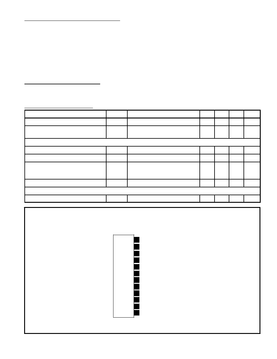
Pin Connection Diagram
(Front View)
V
ref
(40.5V typ) Input
TR1 Source
Error Detection Level
TR1 Gate
TR1 Source
Amplifier Circuit Control
OCP Setting Level Input
Drive Voltage Input
GND
TR1 Drain
No Pin
12
11
TR1 Drain
10
9
8
7
6
5
4
3
2
1
