 | –≠–ª–µ–∫—Ç—Ä–æ–Ω–Ω—ã–π –∫–æ–º–ø–æ–Ω–µ–Ω—Ç: NTE7132 | –°–∫–∞—á–∞—Ç—å:  PDF PDF  ZIP ZIP |

NTE7132
Integrated Circuit
Horizontal and Vertical Deflection Controller
for VGA/XGA and Multi≠Frequency Monitors
Description:
The NTE7132 is an integrated circuit in a 20≠Lead DIP type package. This device is designed to pro-
vide an economical solution in VGA/XGA and multifrequency monitors by incorporating complete
horizontal and vertical small signal processing. VGA≠dependent mode detection and setting are per-
formed on≠chip.
Features:
D
VGA Operation Fully Implemented Including Alignment≠Free Vertical and E/W Amplitude
Pre≠Settings
D
4th VGA Mode Easy Applicable (XGA, Super VGA)
D
Mulit≠Frequency Operation Externally Selectable
D
All Adjustments DC≠Controllable
D
Alignment≠Free Oscillators
D
Sync Separators for Video or Horizontal and Vertical TTL Sync Levels Regardless or Polarity
D
Horizontal Oscillator with P
LL1
for Sync and P
LL2
for Flyback
D
Constant Vertical and E/W Amplitude in Multi≠Frequency Operation
D
Internal Supply Voltage Stabilization with Excellent Ripple Rejection to Ensure Stable Geometrical
Adjustments
Absolute Maximum Ratings:
Supply Voltage (Pin1), V
P
≠0.5 to +16V
. . . . . . . . . . . . . . . . . . . . . . . . . . . . . . . . . . . . . . . . . . . . . . . . . . .
Voltage (Pin3, Pin7), V
3
, V
7
≠0.5 to +16V
. . . . . . . . . . . . . . . . . . . . . . . . . . . . . . . . . . . . . . . . . . . . . . . . . .
Voltage (Pin8), V
8
≠0.5 to +7V
. . . . . . . . . . . . . . . . . . . . . . . . . . . . . . . . . . . . . . . . . . . . . . . . . . . . . . . . . . .
Voltage (Pin5, Pin6, Pin9, Pin10, Pin13, Pin14, Pin18), V
n
≠0.5 to +6.5V
. . . . . . . . . . . . . . . . . . . . . .
Current (Pin2), I
2
±
10mA
. . . . . . . . . . . . . . . . . . . . . . . . . . . . . . . . . . . . . . . . . . . . . . . . . . . . . . . . . . . . . . . .
Current (Pin3), I
3
100mA
. . . . . . . . . . . . . . . . . . . . . . . . . . . . . . . . . . . . . . . . . . . . . . . . . . . . . . . . . . . . . . . .
Current (Pin7), I
7
20mA
. . . . . . . . . . . . . . . . . . . . . . . . . . . . . . . . . . . . . . . . . . . . . . . . . . . . . . . . . . . . . . . . .
Current (Pin8), I
8
≠10mA
. . . . . . . . . . . . . . . . . . . . . . . . . . . . . . . . . . . . . . . . . . . . . . . . . . . . . . . . . . . . . . . .
Electrostatic Handling for All Pins (Note 1), V
esd
±
300V
. . . . . . . . . . . . . . . . . . . . . . . . . . . . . . . . . . . . . .
Operating Junction Temperature, T
J
+150
∞
C
. . . . . . . . . . . . . . . . . . . . . . . . . . . . . . . . . . . . . . . . . . . . . . .
Operating Ambient Temperatrure Range, T
A
0
∞
to +70
∞
C
. . . . . . . . . . . . . . . . . . . . . . . . . . . . . . . . . . . .
Storage Temperature Range, T
stg
≠55
∞
to +150
∞
C
. . . . . . . . . . . . . . . . . . . . . . . . . . . . . . . . . . . . . . . . . .
Thermal Resistance, Junction≠to≠Ambient (In Free Air), R
thJA
65K/W
. . . . . . . . . . . . . . . . . . . . . . . .
Note 1. Equivalent to discharging a 200pF capacitor through a 0
series resistor.
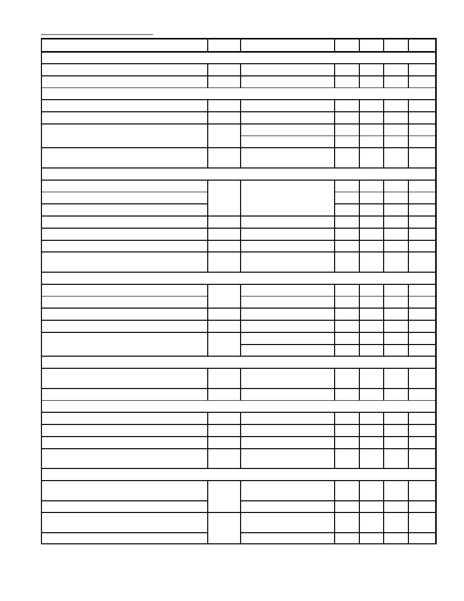
Electrical Characteristics: (V
P
= 12V, T
A
= +25
∞
C unless otherwise specified)
Parameter
Symbol
Test Conditions
Min
Typ
Max
Unit
Supply
Supply Voltage (Pin1)
V
P
9.2
12.0
16.0
V
Supply Current
I
P
≠
40
≠
mA
Internal Reference Voltage
Internal Reference Voltage
V
ref
6.0
6.25
6.5
V
Temperature Coefficient
TC
T
A
= +20
∞
to +100
∞
C
≠
≠
±
90
10
≠6
/K
Power Supply Ripple Rejection
PSRR
f = 1kHz Sine Wave
60
75
≠
dB
f = 1MHz Sine Wave
25
35
≠
dB
Supply Voltage (Pin1) to Ensure All Internal
Reference Voltages
V
P
9.2
≠
16.0
V
Composite Sync Input (AC≠Coupled, V
10
= 5V)
Sync Amplitude of Video Input Signal (Pin9)
V
i sync
Sync on Green, R
S
= 50
≠
300
≠
mV
Top Sync Clamping Level
1.1
1.32
1.5
V
Slicing Level Above Top Sync Level
90
120
150
mV
Allowed Source Resistance for 7% Duty Cycle
R
S
V
i sync
> 200mV
≠
≠
1.5
k
Differential Input Resistance
r
9
During Sync
≠
80
≠
Charging Current of Coupling Capacitor
I
9
V
9
> 1.5V
1.7
2.6
3.4
µ
A
Vertical Sync Integration Time to Generate
Sync Pulse
t
int
7
10
13
µ
s
Horizontal Sync Input (DC≠Coupled, TTL≠Compatible)
Sync Input Signal (Peak Value, Pin9)
V
u sync
1.7
≠
≠
V
Slicing Level
1.2
1.4
1.6
V
Minimum Pulse Width
t
p
700
≠
≠
ns
Rise Time and Fall Time
t
r
, t
f
10
≠
500
ns
Input Current
I
9
V
9
= 0.8V
≠
≠
≠200
µ
A
V
9
5.5V
≠
≠
10
µ
A
Automatic Horizontal Polarity Switch (H≠Sync on Pin9)
Horizontal Sync Pulse Width Related to t
H
(Duty Cycle for Automatic Polarity Correction)
t
p H
/t
H
≠
≠
30
%
Delay Time for Changing Sync Polarity
t
p
0.3
≠
1.8
ms
Vertical Sync Input (DC≠Coupled, TTL≠Compatible,,V≠Sync on Pin10)
Sync Input Signal (Peak Value, Pin10)
V
i sync
1.7
≠
≠
V
Slicing Level
1.2
1.4
1.6
V
Input Current
I
10
0 < V
10
< 5.5V
≠
≠
±
10
µ
A
Maximum Vertical Sync Pulse Width for
Automatic Vertical Polarity Switch
t
p V
≠
≠
300
µ
s
Horizontal Mode Detector Output (VGA Mode)
Output Saturation Voltage LOW
(For Modes 1, 2, and 3)
V
7
I
7
= 6mA
≠
0.275
0.33
V
Output Voltage HIGH
Mode 4
≠
≠
V
P
V
Load Current to Force VGA Mode≠Dependent
Vertical and Parabola Amplitudes
I
7
Modes 1, 2, and 3
2
≠
6
mA
Output Current
Mode 4
≠
0
≠
mA
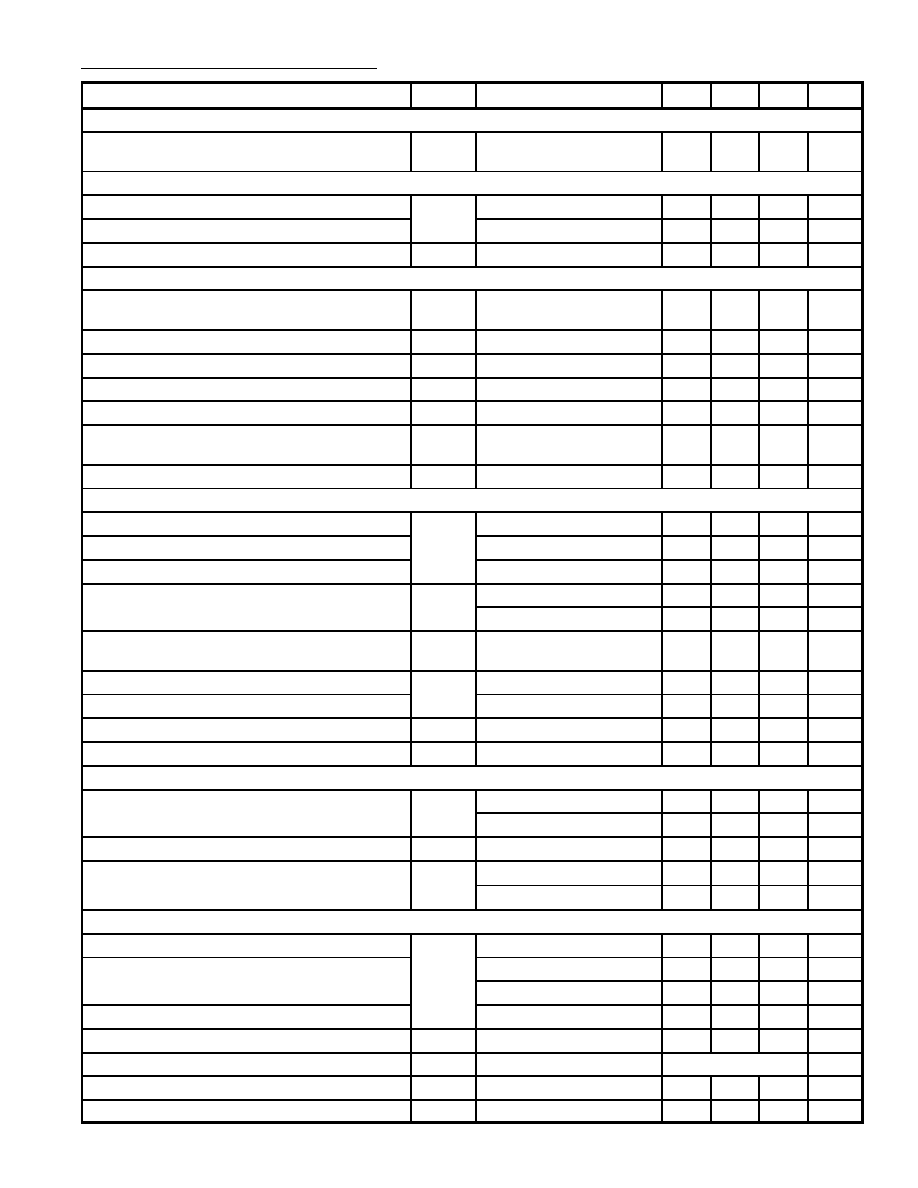
Electrical Characteristics (Cont'd): (V
P
= 12V, T
A
= +25
∞
C unless otherwise specified)
Parameter
Symbol
Test Conditions
Min
Typ
Max
Unit
VGA/Multi≠Frequency Mode Switch
Input Voltage LOW to Force Multi≠Frequency
Mode
V
7
0
≠
50
mV
Horizontal Comparator P
LL1
Upper Control Voltage Limitation
V
17
≠
5.0
≠
V
Lower Control Voltage Limitation
≠
1.2
≠
V
Control Current
I
17
≠
±
300
≠
µ
A
Horizontal Oscillator
Center Frequency
f
OSC
R
18
= 12k
(Pin18),
C
19
= 2.2nF (Pin19)
≠
31.45
≠
kHz
Deviation of Center Frequency
f
OSC
≠
≠
±
3.0
%
Temperature Coefficient
TC
≠
≠
±
150
10
≠6
/K
Relative Holding/Catching Range
H
/t
H
±
6.0
±
6.5
±
7.3
%
External Oscillator Resistor
R
18
9
≠
18
k
Voltage at Reference Current Input (Pin18)
V
18
P
LL1
and P
LL2
Locked,
V
ref
m= 6.25V
≠
3.125
≠
V
Control Voltage
V
18
≠
±
205
≠
mV
Horizontal P
LL2
Upper Clamping Level of Flyback Input
V
2
I
2
= 6mA
≠
5.5
≠
V
Lower Clamping Level of Flyback Input
I
2
= ≠1mA
≠
≠0.75
≠
V
H≠Flyback Slicing Level
≠
3.0
≠
V
Input Current
I
2
H≠Scan; V
8
< 0.9V
≠0.5
≠
≠
mA
H≠Flyback; V
8
> 1.8V
≠
≠
≠0.2
mA
Delay Between Middle of Sync and Middle of
H≠Flyback Related to t
H
t
d
/t
H
≠
3.2
≠
%
Upper Control Voltage Limitation
V
20
≠
4.6
≠
V
Lower Control Voltage Limitation
≠
1.6
≠
V
Control Current
I
20
≠
±
200
≠
µ
A
P
LL2
Control range Related to t
H
t/t
H
30
≠
≠
%
Horizontal Output (Open≠Collector)
Output Voltage LOW
V
3
I
3
= 20mA
≠
≠
0.3
V
I
3
= 60mA
≠
≠
0.8
V
t
H
Duty Cycle
t
p
/t
H
42
45
48
%
Threshold to Activate Too Low Supply Voltage
V
P
Horizontal Output OFF
≠
5.3
≠
V
Protection
Horizontal Output ON
≠
5.6
≠
V
Horizontal Clamping/Blanking Generator Output
Output Voltage LOW
V
8
H and V Scanning
≠
≠
0.9
V
Blanking Output Voltage
Internal V Blanking
1.8
2.1
2.4
V
External H Blanking
1.8
2.1
2.4
V
Clamping Output Voltage
H≠Sync on Pin9
3.5
3.9
4.3
V
Internal Sink Current for All Output Levels
I
8
H and V Scanning
2.3
2.9
3.5
mA
Clamping Pulse Start
t
8
With End of H≠Sync
Clamping Pulse Width
t
clp
0.8
1.0
1.2
µ
s
Steepness of Rise and Fall Times
S
≠
40
≠
ns/V
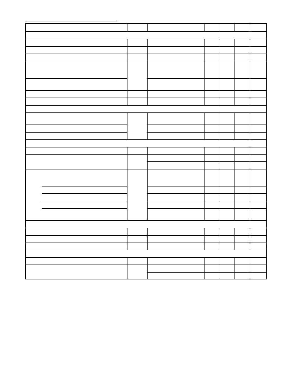
Electrical Characteristics (Cont'd): (V
P
= 12V, T
A
= +25
∞
C unless otherwise specified)
Parameter
Symbol
Test Conditions
Min
Typ
Max
Unit
Vertical Oscillator (V
ref
= 6.25V)
Vertical Free≠Running Frequency
f
o
R
15
= 22k
, C
16
= 0.1
µ
F
40.0
42.0
43.3
Hz
Nominal Vertical Sync Range
f
V
No f
o
Adjustment
50
≠
110
Hz
Voltage on Pin15
V
15
R
15
= 22k
2.8
3.0
3.2
V
Delay Between Sync Pulse and Start of Vertical
Scan in VGA/XGA Mode
t
d
Measured on Pin8,
Activated by an External
Resistor on Pin7
500
575
650
µ
s
Delay Between Sync Pulse and Start of Vertical
Scan in Multi≠Frequency Mode
Measured on Pin8,
V
7
< 50mV
240
300
360
µ
s
Control Current for Amplitude Control
I
12
≠
±
200
≠
µ
A
Capacitor for Amplitude Control
C
12
≠
≠
0.33
µ
F
Vertical Differential Output
Differential Output Current Between Pin5 and
Pin6 (Peak≠to≠Peak Value)
I
o
Mode 3, I
13
> ≠135
µ
A,
R
15
= 22k
0.9
1.0
1.1
mA
Maximum Offset Current Error
I
o
= 1mA
≠
≠
±
2.5
%
Maximum Linearity Error
≠
≠
±
1.5
%
Vertical Amplitude Adjustment (In Percent of Output Signal)
Input Voltage
V
13
≠
5.0
≠
V
Adjustment Current
I
13
I
o
max (100%)
≠110
≠120
≠135
µ
A
I
o
min (Typically 58%)
≠
0
≠
µ
A
VGA Mode≠Dependent Pre≠Settings Activated
by an External Resistor on Pin7
Mode 1
I
o
/
t
Note 2
116.1
116.8
117.5
%
Mode 2
102.0 102.2 102.5
%
Mode 3
≠
100
≠
%
Mode 4
≠
100
≠
%
Multi≠Frequency Operation
(VGA Operation Disabled)
Note 2, V
7
< 50mV
≠
100
≠
%
E/W Output (Note 2)
Bottom Output Signal During Mid≠Scan (Pin11)
V
11
Internally Stabilized
1.05
1.2
1.35
V
Top Output Signal During Flyback
4.1
4.35
4.6
V
Temperature Coefficient of Output Signal
TC
≠
≠
250
10
≠6
/K
E/W Amplitude Adjustment (Parabola)
Input Voltage (Pin14)
V
14
≠
5.0
≠
V
Adjustment Current
I
14
100% Parabola
≠110
≠120
≠135
µ
A
Typicall 28% Parabola
≠
0
≠
µ
A
Note 2.
I
o
/
t relative to value of Mode 3.
Note 3. Parabola amplitude tracks with mode≠dependent vertical amplitude but not with vertical
amplitude adjustment. Tracking can be achieved by a resistor from vertical amplitude
potentiometer to Pin14.

Functional Description:
Horizontal Sync Separator and Polarity Correction
An AC≠coupled video signal or a DC≠coupled TTL sync signal (H only or composite sync) is input
on Pin9. Video signals are clamped with top sync on 12.8V, and are sliced at 1.4V. This results in a
fixed absolute slicing level of 120mV relative to top sync.
DC≠coupled TTL sync signals are also sliced at 1.4V, however with the clamping circuit in current limi-
tation. The polarity of the separated sync is detected by internal integration of the signal, then the po-
larity is corrected.
The polarity information is fed to the VGA mode detector. The corrected sync is the input signal for
the vertical sync integrator and the P
LL1
stage.
Vertical Sync Separator, Polarity Correction and Vertical Sync Integrator
DC≠coupled vertical TTL sync signals may be applied to Pin10. They are sliced at 1.4V. The polarity
of the separated sync is detected by internal integration, then polarity is corrected. The polarity infor-
mation is fed to the VGA mode detector. If Pin10 is not used, it must be connected to GND.
The separated V
i sync
signal from Pin10, or the integrated composite sync signal from Pin9 (TTL or
video) directly triggers the vertical oscillator.
VGA Mode Detector and Mode Output
The three standard VGA modes and a 4th not fixed mode are decoded by the polarities of the horizon-
tal and the vertical sync input signals. An external resistor (from V
P
to Pin7) is necessary to match
this function. In all three VGA modes the correxct amplitudes are activated. The presence of the 4th
mode is indicated by HIGH on Pin7. This signal can be used externally to switch any horizontal or
vertical parameters.
VGA Mode Detector Input
For multi≠frequency operation the voltage on Pin7 must be externally forced to a level of < 50mV. Ver-
tical amplitude pre≠settings for VGA are then inhibited. The delay time between vertical trigger pulse
and the start of vertical deflection changes from 575 to 300
µ
s (575
µ
s is needed for VGA). The vertical
amplitude then remains constant in a frequency range from 50 to 110Hz.
Clamping and Blanking Generator
A combined clamping and blanking pulse is available on Pin8. The lower level of 2.1V can be the
blanking signal derived from line flyback, or the vertical blanking pulse from the internal vertical oscillator.
Vertical blanking equals the delay between vertical sync and the start of vertical scan. By this, an opti-
mum blanking is acheived for VGA/XGA as well as for multi≠frequency operation (selectable via
Pin7).
The upper level of 3.9V is the horizontal clamping pulse with internally fixed pulse width of 1
µ
s. A
mono flop, which is triggered by the trailing edge of the horizontal sync pulse, generates this pulse.
P
LL1
Phase Detector
The phase detector is a standard one using switched current sources. The middle of the sync is
compared with a fixed point of the oscillator sawtooth voltage. The PLL filter is connected to Pin17.
Horizontal Oscillator
This oscillator is a relaxation type oscillator. Its frequency is determined mainly by the capacitor on
Pin19.
A frequency range of one octave is acheived by the current on Pin18. The
1 control voltage from
Pin17 is fed via a buffer amplifier and an attenuator to the current reference Pin18 to acheive a high
DC loop gain. Therefore, changes in frequency will not affect the phase relationship between horizon-
tal sync pulses and line flyback pulses.

Functional Description (Cont'd):
P
LL2
Phase Detector
This phase detector is similar to the P
LL1
phase detector. Line flyback signals (Pin2) are compared
with a fixed point of the oscillator sawtooth voltage. Delays in the horizontal deflection circuit are com-
pensated by adjusting the phase relationship between horizontal sync and horizontal output pulses.
A certain amount of phase adjustment is possible by injecting a DC current froma an external source
into the P
LL2
filter capacitor on Pin20.
Horizontal Driver
This open≠collector output stage (Pin3) can directly drive an external driver transistor. The saturation
voltage is 300mV at 20mA. To protect the line deflection transistor, the horizontal output stage does
not conduct at V
P
< 6.4V (Pin1).
Vertical Oscillator and Amplitude Control
This stage is designed for fast stabilization of the vertical amplitude after changes in sync conditions.
The free≠running frequency f
o
is determined by the values of R
VOS
and C
VOS
. The recommended
values should be altered marginally only to preserve the excellent linearity and noise performance.
The vertical drive currents I
5
and I
6
are in relation to the value of R
VOS
. Therefore, the oscillator fre-
quency must be determined only by C
VOS
on Pin16.
f
o
=
1
10.8 x R
VOS
x C
VOS
To acheive a stabilized amplitude the free≠running frequency f
o
(without adjustment) must be lower
than the lowest occurring sync frequency. The contributions shown in Table 1 can be assumed.
Table 1. Calculation of f
o
Total Spread
Contributing Elements
%
Minimum Frequency Offset Between f
o
and the Lowest Trigger Frequency
10
Spread of IC
±
3
Spread of R (22k
)
±
1
Spread of C (0.1
µ
F)
±
5
Total
19
Results for 50 to 110Hz application: f
o
=
50Hz
1.19
= 42Hz
Table 2. VGA Modes
Mode
Horizontal/Vertical
Sync Polarity
Horizontal
Frequency
(kHz)
Vertical
Frequency
(Hz)
Number of
Active Lines
Output
Mode Pin7
1
+/≠
31.45
70
350
LOW
2
≠/+
31.45
70
400
LOW
3
≠/≠
31.45
60
480
LOW
4
+/+
Fixed by External Circuitry
≠
≠
HIGH
P
LL1
Phase
P
LL2
Phase
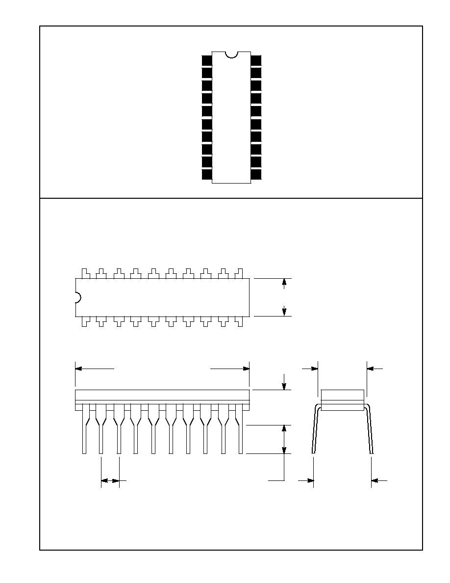
Pin Connection Diagram
E/W Output
E/W Amp Adj Input
Vert OSC Resistor
Vert Sync In
Vert Output 1/Neg≠Going Sawtooth
Vert Amp Adj Input
Horiz Sync/Video In
1
2
3
4
Horiz Flyback Input
Horiz Output
GND (0V)
5
6
7
8
20
19
18
17
Horiz OSC Capacitor
Horiz OSC Resistor
16
Vert OSC Capacitor
15
14
13
Cap for Amp Control
9
12
10
11
V
P
Vert Output 2/Pos≠Going Sawtooth
4th Mode Output/Mode Det Disable In
Clamping/Blanking Pulse Out
.995 (25.3) Max
.280 (7.12) Max
.100 (2.54)
.125 (3.17) Min
.385 (9.8)
.300 (7.62)
.280
(7.1)
1
10
20
11