
NTE7136
Integrated Circuit
Vertical Deflection Power Amplifier for Monitors
Description:
The NTE7136 is a vertical power amplifier for differential input signals in a 9≠Lead SIP type package
suitable for color monitor/TV systems with deflection frequencies up to 140Hz.
Features:
D
Vertical Pre≠Amplifier with Differential Inputs
D
Powerless Vertical Shift
D
Flyback Voltage Generation Suitable for Two Operating Modes (Doubling the Supply Voltage
or External Supply for the Short Flyback Time, this Achieves a Minimum of Power Dissipation)
D
Vertical Output Stage with Thermal and SOAR Protection
D
High Deflection Frequency up to 140Hz
D
High Linear Sawtooth Signal Amplification
D
Possibility of Guarding the Deflection
D
Voltage Stabilizer
Absolute Maximum Ratings: (Voltages referenced to substrate (Pin6) unbless otherwise specified)
Supply Voltage (Pin1), V
P1
40V
. . . . . . . . . . . . . . . . . . . . . . . . . . . . . . . . . . . . . . . . . . . . . . . . . . . . . . . . . .
Supply Voltage (Pin4), V
P2
60V
. . . . . . . . . . . . . . . . . . . . . . . . . . . . . . . . . . . . . . . . . . . . . . . . . . . . . . . . . .
Supply Voltage (Pin8), V
P3
60V
. . . . . . . . . . . . . . . . . . . . . . . . . . . . . . . . . . . . . . . . . . . . . . . . . . . . . . . . . .
Voltage on Pin2, Pin3, and Pin9, V
2
, V
3
, V
9
V
P1
. . . . . . . . . . . . . . . . . . . . . . . . . . . . . . . . . . . . . . . . . . . .
Voltage on Pin5 and Pin7, V
5
, V
7
60V
. . . . . . . . . . . . . . . . . . . . . . . . . . . . . . . . . . . . . . . . . . . . . . . . . . . . .
Current on Pin4, I
4
1A
. . . . . . . . . . . . . . . . . . . . . . . . . . . . . . . . . . . . . . . . . . . . . . . . . . . . . . . . . . . . . . . . . .
Output Current on Pin5 (Peak Value, Note 1), I
5 (M)
±
1.5A
. . . . . . . . . . . . . . . . . . . . . . . . . . . . . . . . . . .
Flyback Current on Pin7 (Peak Value), I
7 (M)
±
1.5A
. . . . . . . . . . . . . . . . . . . . . . . . . . . . . . . . . . . . . . . . .
Current on Pin9, I
9
≠8A
. . . . . . . . . . . . . . . . . . . . . . . . . . . . . . . . . . . . . . . . . . . . . . . . . . . . . . . . . . . . . . . . .
Junction Temperature (Note 1), T
VJ
+168
∞
C
. . . . . . . . . . . . . . . . . . . . . . . . . . . . . . . . . . . . . . . . . . . . . . . .
Operating Ambient Temperatrure Range, T
A
≠20
∞
to +75
∞
C
. . . . . . . . . . . . . . . . . . . . . . . . . . . . . . . . . .
Storage Temperature Range, T
stg
≠25
∞
to +150
∞
C
. . . . . . . . . . . . . . . . . . . . . . . . . . . . . . . . . . . . . . . . . .
Thermal Resistance, Junction≠to≠Mounting Base, R
thJMB
5K/W
. . . . . . . . . . . . . . . . . . . . . . . . . . . . . .
Electrostatic Handling for all Pins (Note 2), V
es
±
300V
. . . . . . . . . . . . . . . . . . . . . . . . . . . . . . . . . . . . . . .
Note 1. Internally limited by thermal protection; switching temperature point at 160
±
8
∞
C
Note 2. Equivalent to discharging a 200pF capacitor throuhg a 0
series resistor.
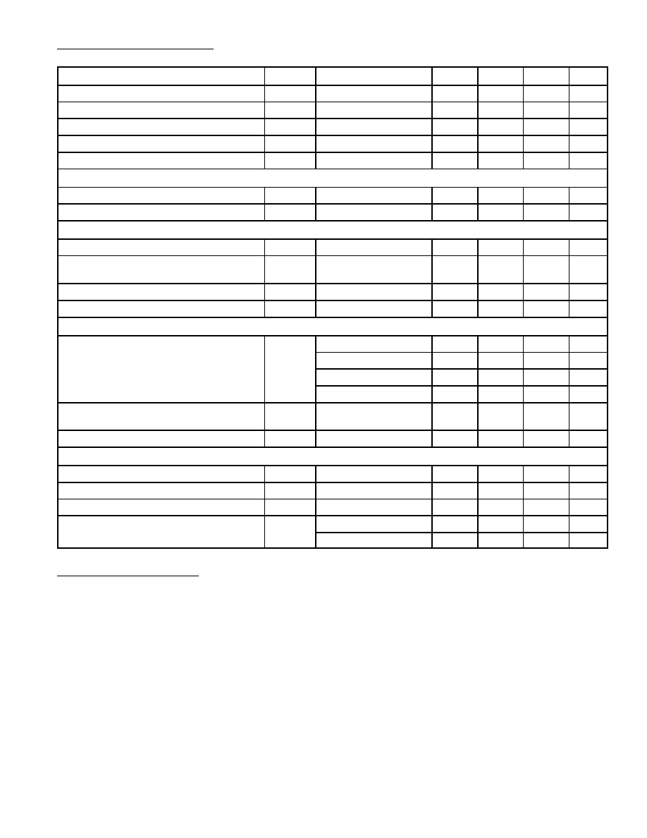
Electrical Characteristics: (V
P1
= V
P2
= 25V, V
N
= V
6
= 0V, T
A
= +25
∞
C, voltages referenced to
substrate (Pin6) unless otherwise specified)
Parameter
Symbol
Test Conditions
Min
Typ
Max
Unit
Supply Voltage 1 (Pin1)
V
P1
9
25
30
V
Supply Voltage 2 (Pin4)
V
P2
9
25
60
V
Supply Voltage 3 (Pin8)
V
P3
9
≠
60
V
Supply Current (Pin1)
I
P1
≠
≠
10
mA
Quiescent Supply Current (Pin4)
I
P2
Without Input Signal
≠
9
≠
mA
Pre≠Amplifier
Input Voltage (Pin2 and Pin3)
V
2
, V
3
1.6
≠
V
P1
≠0.5
V
Input Quiescent Current
I
2
, I
3
Without Input Signal
≠
100
≠
nA
Flyback Generator
Output Voltage
V
7
Upper Value, I
7
= ≠1A
≠
V
P3
≠2.2
≠
V
Flyback Output Current
(Maximum Value, Pin7)
I
7 (M)
≠
≠
±
1.3
A
Threshold Voltage to Switch Flyback
V
1≠5
ON/OFF Threshold
≠
1.4
≠
V
Flyback Pulse Time
t
p FLB
≠
250
≠
µ
s
Vertical Output
Output Voltage
V
5
Upper Value, I
5
= ≠1A
V
P2
≠2.3
V
P2
≠2
≠
V
Lower Value, I
5
= 1A
≠
1.5
1.7
V
Upper Value, I
5
= ≠1.4A
≠
V
P2
≠2.3
≠
V
Lower Value, I
5
= 1.4A
≠
1.7
≠
V
Vertical Output Current
(Peak≠to≠Peak Value, Pin5)
I
5 (P≠P)
≠
≠
2.8
A
Non≠Linearity of Output Signal
LIN
≠
≠
1
%
Pulse Circuit Output
Output Voltage
V
9
R
PCO
= 10k
0.4
≠
V
P1
≠0.4
V
Output Voltage for Thermal Protection Active
V
9
V
P1
≠0.4
≠
≠
V
Voltage to Insert Flyback Pulse on Pin9
V
1≠5
Normal Condition
≠
≠
1.4
V
Pulse Width
t
p9
Deflection Open≠Circuit
≠
50
≠
%
Normal Condition
t
p FLB
≠
≠
µ
s
Functional Description:
Differential Input Amplifier
The differential sawtooth input signal (coming from a ramp output of the NTE7132 for example) is fed
to the input pins 2 and 3. The non≠inverted signal is attached to Pin3. The vertical feedback signal
is superimposed on the inverted input signal on Pin2.
Vertical shift is applied at the inputs in a power≠less way.
Flyback Generator
Signals for the flyback generator and the pulse circuit are generated in the flyback driver stage. The
flyback output consists of a Darlington transistor and a flyback diode. The flyback generator can oper-
ate in two modes:
1. An external supply voltage is applied for the short flyback time, thus power dissipation is minimum.
2. The flyback voltage is generated by doubling the supply voltage. The 100
µ
F capacitor C2 between
Pin4 and Pin7 is charged up to V
P1
during scan, using the external diode and the resistor R2. The
cathode of the capacitor C2 is connected to the positive rail during flyback. Thus, the flyback volt-
age is twice the supply voltage.
Functional Description (Cont'd):
Vertical Output
The vertical output stage is a quasi≠complementary class≠B amplifier with a high linearity. The output
contains SOAR (short≠circuit protection) and thermal protection. The output current on Pin5 is re-
duced for a short time (to let the temperature decrease to T
J
< +150
∞
C), when the junction temperature
(T
J
) exceeds +160
∞
C.
Deflection GUARD
Pin9 will go HIGH if the junction temperature goes too high. A pulse signal with 50% duty cycle is out-
put on Pin9, if the deflection coil is open≠circuit. A flyback pulse signal is output at normal conditions.
Further watching can be achieved by means of an external GUARD circuit. The 22
µ
F capacitor is
charged during flyback time (V
5
> V
8
) at normal conditions. In case of failures, the capacitor is dis-
charged and the GUARD output goes HIGH.
GUARD output level:
D
LOW for normal conditions
D
HIGH for deflection coil short≠circuit respectively open≠circuit
D
HIGH when there are neither input or output signals
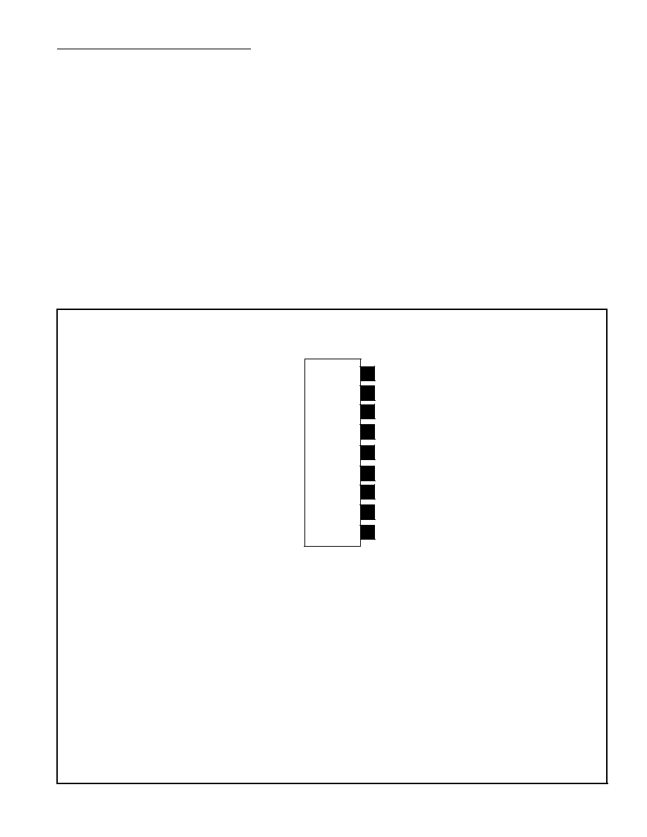
V
P1
V
P2
(Vertical Output Stage)
Vertical Output
Differential Input Amp Input 1
V
P3
(Flyback)
Pulse Circuit Output
Pin Connection Diagram
(Front View)
Substrate
Differential Input Amp Input 2
9
8
7
6
Flyback Generator Output
5
4
3
2
1
