 | –≠–ª–µ–∫—Ç—Ä–æ–Ω–Ω—ã–π –∫–æ–º–ø–æ–Ω–µ–Ω—Ç: NTE7137 | –°–∫–∞—á–∞—Ç—å:  PDF PDF  ZIP ZIP |

NTE7137
Integrated Circuit
Advanced Monitor Video Controller
Description:
The NTE7137 is a monolithic integrated RGB amplifier in a 20≠Lead DIP type package designed for
color monitor systems with super VGA performance. It is intended for DC or AC coupling of the color
signals to the cathodes of a CRT.
Features:
D
Fully DC Controllable
D
3 Separate Video Channels
D
Input Black Level Clamping
D
White Level Adjustment for 2 Channels Only
D
Brightness Control with Correct Grey Scale Tracking
D
Contrast Control for All 3 Channels Simultaneously
D
Cathode Feedback to Internal Reference for Cut≠Off Control, Which Allows Unstabilized Video
Supply Voltage
D
Current Outputs for RGB Signal Currents
D
RGB Voltage Outputs to External Peaking Circuits
D
Blanking and Switch≠Off Input for Screen Protection
D
Sync On Green Operation Possible
Absolute Maximum Ratings:
Supply Voltage (Pin7), V
P
0 to +8.8V
. . . . . . . . . . . . . . . . . . . . . . . . . . . . . . . . . . . . . . . . . . . . . . . . . . . . .
Input Voltage Range (Pin2, Pin5, Pin8), V
i
≠0.1 to V
P
. . . . . . . . . . . . . . . . . . . . . . . . . . . . . . . . . . . . . . .
External DC Voltage Ranges, V
ext
Pin14, Pin17, Pin14
≠0.1 to V
P
. . . . . . . . . . . . . . . . . . . . . . . . . . . . . . . . . . . . . . . . . . . . . . . . . . . .
Pin13, Pin16, Pin19
No External Voltages
. . . . . . . . . . . . . . . . . . . . . . . . . . . . . . . . . . . . . . . . . . .
Pin1, Pin3, Pin6, Pin11
≠0.1 to V
P
. . . . . . . . . . . . . . . . . . . . . . . . . . . . . . . . . . . . . . . . . . . . . . . . . .
Pin9
≠0.1 to V
P
+0.7V
. . . . . . . . . . . . . . . . . . . . . . . . . . . . . . . . . . . . . . . . . . . . . . . . . . . . . . . . . . . . .
Pin10
≠0.1 to V
P
+0.7V0
. . . . . . . . . . . . . . . . . . . . . . . . . . . . . . . . . . . . . . . . . . . . . . . . . . . . . . . . . . .
Average Output Current (Pin14, Pin17, Pin20), I
o
0 to 50mA
. . . . . . . . . . . . . . . . . . . . . . . . . . . . . . . . .
Peak Output Current (Pin14, Pin17, Pin20), I
M
0 to 100mA
. . . . . . . . . . . . . . . . . . . . . . . . . . . . . . . . . .
Total Power Dissipation, P
tot
1200mW
. . . . . . . . . . . . . . . . . . . . . . . . . . . . . . . . . . . . . . . . . . . . . . . . . . . .
Electrostatic Handling for All Pins (Note 1), V
esd
±
500V
. . . . . . . . . . . . . . . . . . . . . . . . . . . . . . . . . . . . . .
Operating Junction Temperature Range, T
J
≠25
∞
to +150
∞
C
. . . . . . . . . . . . . . . . . . . . . . . . . . . . . . . . . .
Operating Ambient Temperatrure Range, T
A
0
∞
to +70
∞
C
. . . . . . . . . . . . . . . . . . . . . . . . . . . . . . . . . . . .
Storage Temperature Range, T
stg
≠25
∞
to +150
∞
C
. . . . . . . . . . . . . . . . . . . . . . . . . . . . . . . . . . . . . . . . . .
Thermal Resistance, Junction≠to≠Ambient (In Free Air), R
thJA
65K/W
. . . . . . . . . . . . . . . . . . . . . . . .
Note 1. Equivalent to discharging a 200pF capacitor through a 0
series resistor.

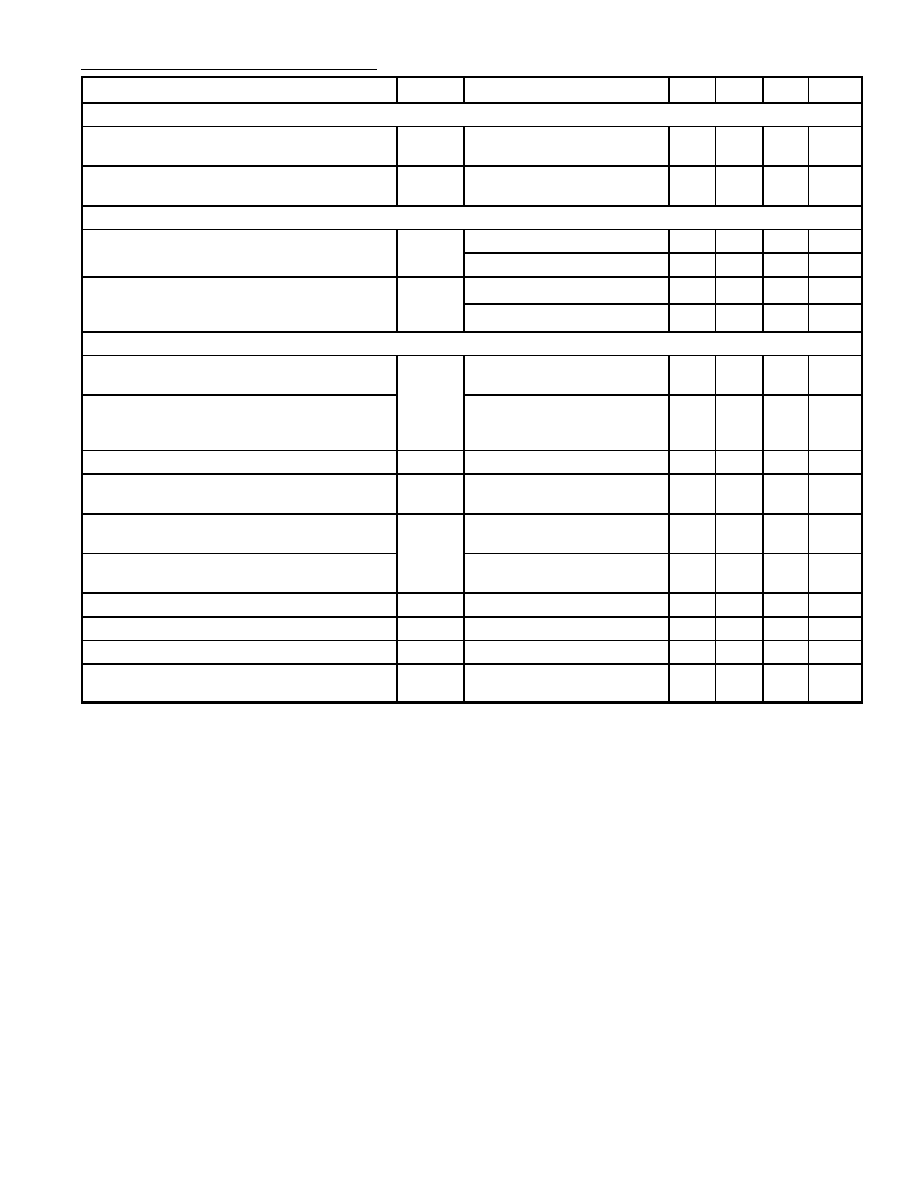
Electrical Characteristics: (V
P
= 8V, T
A
= +25
∞
C, Note 2 unless otherwise specified)
Parameter
Symbol
Test Conditions
Min
Typ
Max
Unit
Supply
Supply Voltage Range (Pin7)
V
P
7.2
8.0
8.8
V
Supply Current (Pin7)
I
P
≠
46
56
mA
Video Signal Inputs
Input Voltage (Black≠to≠White, Pin2, Pin5, Pin8)
V
I(b≠w)
≠
0.7
1.0
V
DC Current
I
2, 5, 8
No Clamping
≠0.1
≠
+0.1
µ
A
During Clamping
±
50
≠
≠
µ
A
Brightness Control
Input Voltage Range
V
1
Note 3
1.0
≠
6.0
V
Input Resistance to V
N1
R
1
≠
50
≠
k
Black Level Voltage Change at Nominal Gain
V
bl1
V
1
= 1V, V
3, 11
Open≠Circuit
≠
≠80
≠
mV
(Pin19, Pin16, Pin13)
V
1
= 6V, V
3, 11
Open≠Circuit
≠
240
≠
mV
Input Voltage for Nominal Brightness
V
N1
Pin1 Open≠Circuit
≠
2.25
≠
V
Contrast Control (Note 4)
Input Voltage Range
V
6
Note 3
1.0
≠
6.0
V
Current
I
6
≠5
≠1
≠
µ
A
Contrast Relative to Nominal Contrast
C
v
V
1
= 6V, V
3, 11
Open≠Circuit
≠
3
≠
dB
V
1
= 4.5V, V
3, 11
Open≠Circuit
≠
0
≠
dB
V
1
= 1V, V
3, 11
Open≠Circuit
≠
≠20
≠
dB
Tracking of RGB Signals
T
r
2.5V < V
6
< 6V,
V
3, 11
Open Circuit
≠
0
0.5
dB
Gain Control
Input Voltage Range
V
3, 11
Note 3
1.0
≠
6.0
V
Input Resistance Against V
N3, N11
R
3, 11
≠
43
≠
k
Gain Relative to Nominal Gain
G
v
V
6
= 4.5V, V
3, 11
= 6V
≠
2
≠
dB
V
6
= 4.5V, V
3, 11
= 1V
≠
≠4
≠
dB
Input Voltage for Nominal Gain
V
N3, N11
Pin3, Pin11 Open Circuit
≠
4.6
≠
V
Feedback Input
Input Voltage Range
V
3, 11
Note 5
tbn
5.8
tbn
V
Output Current
I
18, 15, 12
During Output Clamping
≠1.5
≠1.0
≠0.1
µ
A
Voltage Outputs (Pin19, Pin16, Pin13)
Signal Output Voltage (Black≠to≠White Value)
V
O(b≠w)
V
3, 11
Open, V
6
= 4.5V,
V
I(b≠w)
= 0.7V
≠
0.8
≠
V
Black Level Voltage
V
bl
During Output Clamping,
Depending on Black Level
Adjustment, Note 6
0.3
≠
1.0
V
During Switch≠Off
≠
0.1
0.3
V
Signal≠to≠Noise Ratio
S/N
≠
≠
44
dB
Note 2. All voltages measured to GND (Pin4).
Note 3. Typical range is 1 to 6V, the range can be increased (e.g. 0 to 7V) to slightly increase the
control range.
Note 4. Open contrast control pin leads to undefined contrast setting.
Note 5. The internal reference voltage can be measured at Pin18, Pin15, and Pin12 during output
clamping in closed feedback loop.
Note 6. Minimum guaranteed control range, the typical minimum black level voltage is 0.1V.
Electrical Characteristics (Cont'd): (V
P
= 8V, T
A
= +25
∞
C, Note 2 unless otherwise specified)
Parameter
Symbol
Test Conditions
Min
Typ
Max
Unit
Frequency Response at Voltage Outputs
Gain Decreases by Frequency Response at
Pin19, Pin16, Pin13
G
vf
70MHz
≠
≠
≠3
dB
Rise Time at Voltage Output
(Pin19, Pin16, Pin13)
t
rO
10% to 90% Amplitude,
Input Rise Time = 1ns
≠
4.5
5.0
ns
Current Outputs (Pin20, Pin17, Pin14)
Signal Current (Black≠to≠White)
I
O(b≠w)
≠
50
≠
mA
With Peaking, Note 7
≠
≠
100
mA
HF Saturation of Output Transistors
V
20≠19,
I
O
= 50mA
≠
≠
2.0
V
17≠16,
14.13
I
O
= 100mA
≠
≠
2.2
V
Threshold Voltages (Note 8)
Threshold for Horizontal Blanking
(Blanking, Output Clamping)
V
9
1.2
1.4
1.6
V
Threshold for Switch≠Off
(Blanking, Minimum Black Level, No
Output Clamping)
5.8
6.5
6.8
V
Input Resistance Referenced to GND
R
g
50
80
110
k
Delay Between Horizontal Blanking Input
and Output Signal Blanking
t
d9
≠
35
60
ns
Threshold for Vertical Blanking
(Blanking, No Input Clamping)
V
10
1.2
3.0
3.5
V
Threshold for Clamping
(Input Clamping, No Blanking)
2.6
3.0
3.5
V
Input Current
I
10
≠3
≠1
≠
µ
A
Rise and Fall Time for Clamping Pulse
t
r, f10
Transition 1 to 3.5V
≠
≠
75
ns/V
Clamping Pulse Width
t
w10
V
10
= 3V
0.6
≠
≠
µ
s
Delay Between Vertical Blanking Input
and Output Signal Blanking
t
d10
≠
300
≠
ns
Note 2. All voltages measured to GND (Pin4).
Note 7. The external RC combination at Pin19, Pin16 and Pin13 enables peak currents during transients.
Note 8. The internal threshold voltages are derived from an internally stabilized voltage. The internal
pulses are generated if the input pulses are higher than the thresholds.

Functional Description:
RGB input signals (0.7V
P≠P
) are capacitively coupled into the NTE7137 (Pin2, Pin5, and Pin8) from
a low ohmic source and are clamped to an internal DC voltage (artificial balck level). Composite sig-
nals will not disturb normal operations because an internal clipping circuit cuts all signal parts below
black level. Channes 1 and 3 have a maximum total voltage gain of 6dB (maximum contrast and maxi-
mum individual channel gain), Channel 2 of 4dB (maximum contrast and nominal channel gain). With
the nominal channel gain of 1dB and nominal contrast setting the nominal black≠to≠white output am-
plitude is 0.8V
P≠P
.
DC voltages are used for brightness, contrast and gain control. Brightness control yeilds a simulta-
neous signal black level shift of the three channels relative to a reference black level. For nominal
brightness (Pin1 open≠circuit) the signal black level is equal to the reference black level.
Contrast control is achieved by a voltage at Pin6 and affects the three channels simultaneously.
To provide the correct white point, an individual gain control (Pin3 and Pin11) adjusts the signals of
Channels 1 and 3 compared to the reference Channel 2. Gain setting affects contrast and brightness
to achieve correct grey scale tracking.
Each output stage provides a current output (Pin20, Pin17 and Pin14) and a voltage output (Pin19,
Pin16 and Pin13). External cascode transistors reduce power consumption of the IC and prevent
breakdown of the output transistors. Signal output currents and peaking characteristics are deter-
mined by external components at the voltage outputs and the video supply.
The three channels have separate internal feedback loops which ensure large signal linearity and
marginal signal distortion in spite of output transistor thermal V
BE
variation.
The clamping pulse (Pin10) is used for input clamping only. The input signals have to be at black level
during the clamping pulse and are clamped to an internal artificial black level. The coupling capacitors
are used in this way for black level storage. Because the threshold for the clamping pulse is higher
than that for vertical blanking (Pin10) the rise and fall times of the clamping pulse have to be faqster
than 75ns/V (1V to 3.5V).
The vertical blanking pulse will be detected if the input voltage (Pin10) is higher than the threshold
voltage for approximately 300ns but does not exceed the threshold for the clamping pulse in the time
between. During the vertical blanking pulse the input clamping is disabled to avoid misclamping in
the event of composite input signals. The input signal is blanked and the artificial black level is inserted
instead. Additionally the brightness is internally set to its nominal value, thus the output signal is at
reference black levels. The DC value of the reference black level will be adjusted by cut≠off stabiliza-
tion.
During horizontal blanking (Pin9) the output signal is set to reference black level as previously de-
scribed and output clamping is activated. If the voltage at Pin9 exceeds the switch off threshold the
signal is blanked and switched to ultra black level for screen protection and spot suppression during
V≠flyback. Ultra black level is the lowest possible output voltage (at voltage outputs) and does not
depend on cut≠off stabilization.
For cut≠off stabilization (DC coupling to the CRT) respectively black level stabilization (AC couplking)
the video signal at the cathode or the coupling capacitor is divided by an adjustable voltage divider
and fed to the feedback inputs (Pin18, Pin15 and Pin12). During horizontal blanking time this signal
is compared with an internal DC voltage of approzimately 5.8V. Any difference will lead to a reference
black level correction by charging or discharging the integrated capacitor which stores the reference
black level information between the horizontal blanking pulses.

Current Output Ch2
Current Output Ch1
Pin Connection Diagram
Gain Control Ch3
Feedback Ch2
Input Clamping, Vertical Blanking
Signal Input Ch2
Voltage Output Ch3
Horizontal Blanking, Swith Off
1
2
3
4
Brightness Control
Signal Input Ch1
Gain Control Ch1
GND
5
6
7
8
20
19
18
17
Voltage Output Ch1
Feedback Ch1
16
Voltage Output Ch2
15
14
13
Feedback Ch3
9
12
10
11
Contrast Control
Signal Input Ch3
.995 (25.3) Max
.280 (7.12) Max
.100 (2.54)
.125 (3.17) Min
.385 (9.8)
.300 (7.62)
.280
(7.1)
1
10
20
11
V
P
Current Output Ch3