NTE7147
Integrated Circuit
Full Bridge Current Driven Vertical Deflection Booster
Description:
The NTE7147 is a power amplifier in a 9≠Lead SIP type package designed for use in 90 degree color
vertical deflection systems for frame frequencies of 50Hz to 160Hz. This device provides a high
CMRR current driven differential input. Due to the bridge configuration of the two output stages, DC≠
coupling of the deflection coil is achieved.
Features:
D
Pre≠Amplifier with Differential High CMRR Current Mode Inputs
D
Low Offsets
D
High Linear Sawtooth Signal Amplification
D
High Efficient DC≠Coupled Vertical Output Bridge Circuit
D
Powerless Vertical Shift
D
High Deflection Frequency up to 160Hz
D
Power Supply and Flyback Supply Voltage Independent Adjustable to Optimize Power
Consumption and Flyback Time
D
Excellent Transition Behaviour Duriing Flyback
D
Guard Circuit for Screen Protection
Absolute Maximum Ratings: (Voltage referenced to Pin5 (GND) unless otherwise specified)
Supply Voltage (Pin3), V
P
30V
. . . . . . . . . . . . . . . . . . . . . . . . . . . . . . . . . . . . . . . . . . . . . . . . . . . . . . . . . . .
Flyback Supply Voltage (Pin7), V
FB
60V
. . . . . . . . . . . . . . . . . . . . . . . . . . . . . . . . . . . . . . . . . . . . . . . . . . .
Flyback Supply Current, I
FB
±
1.8A
. . . . . . . . . . . . . . . . . . . . . . . . . . . . . . . . . . . . . . . . . . . . . . . . . . . . . . .
Input Voltage, V
1
, V
2
0 to V
P
V
. . . . . . . . . . . . . . . . . . . . . . . . . . . . . . . . . . . . . . . . . . . . . . . . . . . . . . . . . . .
Input Current, I
1
, I
2
0 to
±
5mA
. . . . . . . . . . . . . . . . . . . . . . . . . . . . . . . . . . . . . . . . . . . . . . . . . . . . . . . . . . .
Output Voltage, V
4
, V
6
0 to V
P
V
. . . . . . . . . . . . . . . . . . . . . . . . . . . . . . . . . . . . . . . . . . . . . . . . . . . . . . . . .
Output Current (Note 1), I
4
, I
6
0 to
±
1.8A
. . . . . . . . . . . . . . . . . . . . . . . . . . . . . . . . . . . . . . . . . . . . . . . . . .
Feedback Voltage, V
9
0 to V
P
V
. . . . . . . . . . . . . . . . . . . . . . . . . . . . . . . . . . . . . . . . . . . . . . . . . . . . . . . . . .
Feedback Current, I
9
0 to
±
5mA
. . . . . . . . . . . . . . . . . . . . . . . . . . . . . . . . . . . . . . . . . . . . . . . . . . . . . . . . .
Guard Voltage (Note 2), V
8
0 to V
P
+0.4V
. . . . . . . . . . . . . . . . . . . . . . . . . . . . . . . . . . . . . . . . . . . . . . . . . .
Guard Current, I
8
0 to
±
5mA
. . . . . . . . . . . . . . . . . . . . . . . . . . . . . . . . . . . . . . . . . . . . . . . . . . . . . . . . . . . . .
Operating Junction Temperature Range (Note 3), T
J
≠20
∞
to +150
∞
C
. . . . . . . . . . . . . . . . . . . . . . . . . .
Ambient Temperature Range, T
A
≠20
∞
to +75
∞
C
. . . . . . . . . . . . . . . . . . . . . . . . . . . . . . . . . . . . . . . . . . . .
Storage Temperature Range, T
stg
≠20
∞
to +150
∞
C
. . . . . . . . . . . . . . . . . . . . . . . . . . . . . . . . . . . . . . . . . .
Thermal Resistance, Junction≠to≠Mounting Base, R
thJ≠MB
4K/W
. . . . . . . . . . . . . . . . . . . . . . . . . . . . .
Electrostatic Handling Voltage (Note 4), V
es
≠500V to +500V
. . . . . . . . . . . . . . . . . . . . . . . . . . . . . . . .
Note 1. Maximum output currents I
4
and I
6
are limited by current protection.
Note 2. For V
P
> 13V, the guard voltage V
8
is limited to 13V.
Note 3. Internally limited by thermal protection; switching point
+150
∞
C.
Note 4. Equivalent to discharging a 200pF capacitor through a 0
series resistor,

D
i
=
x
with I
deflc
= common mode deflection current and I
idc
= common mode
I
deflc
I
idc
I
id
I
defl
input current.
Electrical Characteristics: (V
P
= 15V, T
A
= +25
∞
C, V
FB
= 40V, voltage referenced to Pin5 (GND)
unless otherwise specified)
Parameter
Symbol
Test Conditions
Min
Typ
Max
Unit
Supply Voltage (Pin3)
V
P
8.2
≠
25
V
Flyback Supply Voltage (Pin7)
V
FB
Note 5
V
P
+6
≠
60
V
Quiescent Feedback Current (Pin7)
I
FB
No Load, No Signal
≠
7
10
mA
Input Stage
Differential Input Current (I
id
= I
1
≠ I
2
)
(Peak≠to≠Peak Value)
I
id(p≠p)
≠
±
500
±
600
µ
A
Single Ended Input Current
(Peak≠to≠Peak Value)
I
1,2(p≠p)
Note 6
0
±
300
±
600
µ
A
Common Mode Rejection Ratio
CMRR
Note 7
≠
≠54
≠
dB
Input Clamp Voltage
V
1
I
1
= 300
µ
A
2.7
3.0
3.3
V
V
2
I
2
= 300
µ
A
2.7
3.0
3.3
V
Input Clamp Signal TC on Pin1
TC
i,1
0
≠
±
800
µ
V/K
Input Clamp Signal TC on Pin2
TC
i,2
0
≠
±
800
µ
V/K
Differential Input Voltage
V
1
≠ V
2
I
id
= 0
0
≠
±
10
mV
Feedback Current
I
9
≠
±
500
±
600
µ
A
Feedback Voltage
V
9
1
≠
V
P
≠1
V
Differential Input Offset Current
(I
id(offset)
= I
1
≠ I
2
)
I
id(offset)
I
defl
= 0, R
ref
= 1.5k
, R
m
= 1
0
≠
±
20
µ
A
Input Capacity Pin1 Reference to GND
C
i INA
≠
≠
5
pF
Input Capacity Pin2 Reference to GND
C
i INB
≠
≠
5
pF
Output Stages A and B
Output Current
I
4
, I
6
≠
≠
±
1
A
Output A Saturation Voltage to GND
V
6
I
6
= 0.7A
≠
1.3
1.5
V
I
6
= 1.0A
≠
1.6
1.8
V
Output A Saturation Voltage to V
P
V
6,3
I
6
= 0.7A
≠
2.3
2.9
V
I
6
= 1.0A
≠
2.7
3.3
V
Output B Saturation Voltage to GND
V
4
I
4
= 0.7A
≠
1.3
1.5
V
I
4
= 1.0A
≠
1.6
1.8
V
Output B Saturation Voltage to V
P
V
4,3
I
4
= 0.7A
≠
1.0
1.6
V
I
4
= 1.0A
≠
1.3
1.9
V
Linearity Error
LE
I
defl
=
±
0.7A, Note 8
≠
≠
2
%
Note 5. Up to 60V
V
FB
40V a decoupling capacitor C
FB
= 22
µ
(between Pin7 and Pin5) and a resistor
R
FB
= 100
(between Pin7 and V
FB
) are required.
Note 6. Saturation voltages of output stages A and B can be increased in the event of negative input
currents I
1,2
< ≠500
µ
A.
Note 7.
Note 8. Deviation of the output slope at a constant input slope.

Electrical Characteristics (Cont'd): (V
P
= 15V, T
A
= +25
∞
C, V
FB
= 40V, voltage referenced to
Pin5 (GND) unless otherwise specified)
Parameter
Symbol
Test Conditions
Min
Typ
Max
Unit
Output Stages A and B (Cont'd)
DC Output Voltage
V
4
, V
6
I
id
= 0A, Closed≠Loop
6.6
7.2
7.8
V
Open≠Loop Current Gain (I
4, 6
/I
id
)
G
oi
I
4, 6
< 100mA, Note 9
≠
100
≠
dB
Open≠Loop Current Gain (I
4, 6
/I
9
)
G
ofb
I
4, 6
< 100mA, Note 9
≠
100
≠
dB
Current Ratio (I
id
/I
9
)
G
ifb
Closed≠Loop
≠
≠0.2
≠
dB
Output Ripple Current as a Function
of Supply Ripple
I
defl(ripple)
V
P(ripple)
=
±
0.5V, I
id
= 0,
Closed≠Loop
≠
±
1
≠
mA
Flyback Generator
Voltage Drop During Flyback
Reverse
V
7, 6
I
defl
= 0.7A
≠
≠2.0
≠3.0
V
defl
= 1.0A
≠
≠2.3
≠3.5
V
Forward
defl
= 0.7A
≠
+5.6
+6.1
V
defl
= 1.0A
≠
+5.9
+6.5
V
Switching On Threshold Voltage
V
6
V
P
≠1
≠
V
P
+1.5
V
Switching Off Threshold Voltagte
V
6
V
p
≠1.5
≠
V
P
+1
V
Flyback Current During Flyback
I
7
≠
≠
±
1
A
Guard Circuit
Output Voltage
V
8
Guard On
7.5
8.5
10
V
Guard On, V
P
= 8.2V
6.9
≠
V
P
≠0.4
V
Guard Off
≠
≠
0.4
V
Output Current
I
8
Guard On
5
≠
≠
mA
Guard Off, V
8
= 5V
0.5
1.0
1.5
mA
Allowable External Voltage on Pin8
V
8(ext.)
0
≠
13
V
V
P
13V
0
≠
V
P
+0.3
V
Note 9. Frequency behaviour of G
oi
and G
ofb
.
a) ≠3dB open≠loop bandwidth (≠45
∞
) at 15kHz; second pole (≠135
∞
) at 1.3MHz.
b) Open≠loop gain at second pole (≠135
∞
) 55dB.
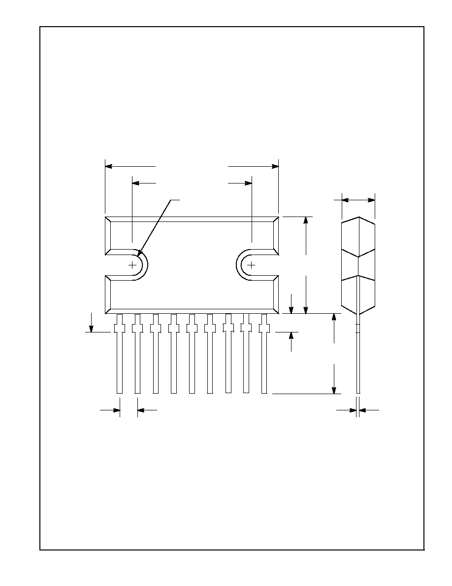
V
P
Pin Connection Diagram
(Front View)
Flyback Supply Voltage
Feedback Input
Output B
Input B
GND
Guard Output
Output A
Input A
9
8
7
6
5
4
3
2
1