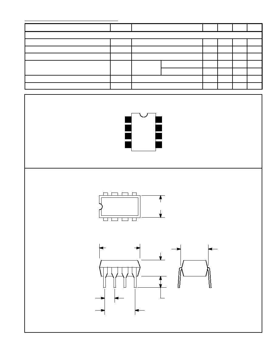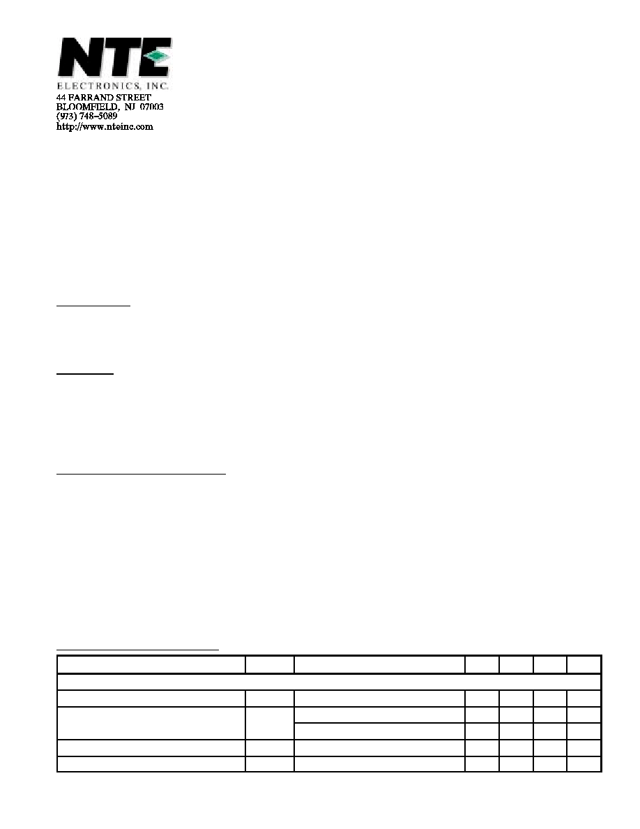
NTE7155
Integrated Circuit
Dual Low≠Voltage Power Amplifier
Description:
The NTE7155 is a monolithic integrated circuit in an 8≠Lead DIP type package designed for use as
a dual audio power amplifier in portable cassette players and radios.
Features:
D
Supply Voltage Down To 1.8V
D
Low Crossover Distortion
D
Low Quiescent Current
D
Bridge or Stereo Configuration
Absolute Maximum Ratings:
Supply Voltage, V
S
15V
. . . . . . . . . . . . . . . . . . . . . . . . . . . . . . . . . . . . . . . . . . . . . . . . . . . . . . . . . . . . . . . . .
Peak Output Current, I
O
1A
. . . . . . . . . . . . . . . . . . . . . . . . . . . . . . . . . . . . . . . . . . . . . . . . . . . . . . . . . . . . . .
Total Power Dissipation, P
D
T
A
= +50
∞
C
1.0W
. . . . . . . . . . . . . . . . . . . . . . . . . . . . . . . . . . . . . . . . . . . . . . . . . . . . . . . . . . . . . . . . .
T
C
= +50
∞
C
1.4W
. . . . . . . . . . . . . . . . . . . . . . . . . . . . . . . . . . . . . . . . . . . . . . . . . . . . . . . . . . . . . . . . .
Operating Junction Temperature Range, T
J
≠40
∞
to +150
∞
C
. . . . . . . . . . . . . . . . . . . . . . . . . . . . . . . . . .
Storage Temperature Range, T
stg
≠40
∞
to +150
∞
C
. . . . . . . . . . . . . . . . . . . . . . . . . . . . . . . . . . . . . . . . . .
Thermal Resistance, Junction≠to≠Ambient, R
thJA
100
∞
C/W
. . . . . . . . . . . . . . . . . . . . . . . . . . . . . . . . . .
Thermal Resistance, Junction≠to≠Case (Pin4), R
thJC
70
∞
C/W
. . . . . . . . . . . . . . . . . . . . . . . . . . . . . . .
Electrical Charactgeristics: (V
S
= 6V, T
A
= +25
∞
C unless otherwise specified)
Parameter
Symbol
Test Conditions
Min
Typ
Max
Unit
Stereo
Supply Voltage
V
S
1.8
≠
15
V
Quiescent Output Voltage
V
O
≠
2.7
≠
V
V
S
= 3V
≠
1.2
≠
V
Quiescent Drain Current
I
D
≠
6
9
mA
Input Bias Current
I
B
≠
100
≠
nA
Electrical Charactgeristics (Cont'd): (V
S
= 6V, T
A
= +25
∞
C unless otherwise specified)
Parameter
Symbol
Test Conditions
Min
Typ
Max
Unit
Stereo (Cont'd)
Output Power (Each Channel)
P
O
R
L
= 32
V
S
= 9V
≠
300
≠
mW
(f = 1kHz, d = 10%)
V
S
= 6V
90
120
≠
mW
V
S
= 4.5V
≠
60
≠
mW
V
S
= 3V
15
20
≠
mW
V
S
= 2V
≠
5
≠
mW
R
L
= 16
V
S
= 6V
170
220
≠
mW
R
L
= 8
V
S
= 9V
≠
1000
≠
mW
V
S
= 6V
300
380
≠
mW
R
L
= 4
V
S
= 6V
450
650
≠
mW
V
S
= 4.5V
≠
320
≠
mW
V
S
= 3V
≠
110
≠
mW
Distortion (f = 1kHz)
d
R
L
= 32
, P
O
= 40mW
≠
0.2
≠
%
R
L
= 16
, P
O
= 75mW
≠
0.2
≠
%
R
L
= 8
, P
O
= 150mW
≠
0.2
≠
%
Closed Loop Voltage Gain
G
V
f = 1kHz
36
39
41
dB
Channel Balance
G
V
≠
≠
±
1
dB
Input Resistance
R
I
f = 1kHz
100
≠
≠
k
Total Input Noise
e
N
R
S
= 10k
B = Curve A
≠
2.0
≠
µ
V
B = 22Hz to 22kHz
≠
2.5
≠
µ
V
Supply Voltage Rejection
SVR
f = 100Hz, C1 = C2 = 100
µ
F
24
30
≠
dB
Channel Separation
C
S
f = 1kHz
≠
50
≠
dB
Bridge
Supply Voltage
V
S
1.8
≠
15
V
Quiescent Drain Current
I
D
R
L
=
≠
6
9
mA
Output Offset Voltage (Between Outputs)
V
OS
R
L
= 8
≠
≠
±
50
mV
Input Bias Current
I
B
≠
100
≠
nA
Output Power (f = 1kHz, d = 10%)
P
O
R
L
= 32
V
S
= 9V
≠
1000
≠
mW
V
S
= 6V
320
400
≠
mW
V
S
= 4.5V
≠
200
≠
mW
V
S
= 3V
50
65
≠
mW
V
S
= 2V
≠
8
≠
mW
R
L
= 16
V
S
= 9V
≠
2000
≠
mW
V
S
= 6V
≠
800
≠
mW
V
S
= 3V
≠
120
≠
mW
R
L
= 8
V
S
= 6V
900
1350
≠
mW
V
S
= 4.5V
≠
700
≠
mW
V
S
= 3V
≠
220
≠
mW
R
L
= 4
V
S
= 4.5V
≠
1000
≠
mW
V
S
= 3V
200
350
≠
mW
V
S
= 2V
≠
80
≠
mW