
NTE7156
Integrated Circuit
DCÙCoupled Vertical Deflection Circuit
Description:
The NTE7156 is a power circuit in a 9ÙLead SIP type package designed for use in 90
¯
and 110
¯
color
deflection systems for field frequencies of 50Hz to 120Hz. This device provides a DC driven vertical
deflection output circuit, operating as a highly efficient class G system.
Features:
D
Few External Components
D
Highly Efficient Fully DCÙCoupled Vertical Output Bridge Circuit
D
Vertical Flyback Switch
D
Guard Circuit
D
Protection Aaginst:
Ù ShortÙCircuit of the Output Pins (7 and 4)
Ù ShortÙCircuit of the Output Pins to V
P
D
Temperature Protection
D
High EMC Immunity Because of Common Mode Inputs
D
A Guard Signal in Zoom Mode
Absolute Maximum Ratings:
DC Supply
Supply Voltage, V
P
NonÙOperating
40V
. . . . . . . . . . . . . . . . . . . . . . . . . . . . . . . . . . . . . . . . . . . . . . . . . . . . . . . . . . . . . .
Operating
25V
. . . . . . . . . . . . . . . . . . . . . . . . . . . . . . . . . . . . . . . . . . . . . . . . . . . . . . . . . . . . . . . . . . .
Flyback Supply Voltage, V
FB
50V
. . . . . . . . . . . . . . . . . . . . . . . . . . . . . . . . . . . . . . . . . . . . . . . . . . . . . . . . .
Note 1
60V
. . . . . . . . . . . . . . . . . . . . . . . . . . . . . . . . . . . . . . . . . . . . . . . . . . . . . . . . . . . . . . . . . . . . . .
Vertical Circuit
Output Current (PeakÙtoÙPeak Value, Note 2), I
O(PÙP)
3A
. . . . . . . . . . . . . . . . . . . . . . . . . . . . . . . . . . .
Output Voltage (Pin7), V
O(A)
52V
. . . . . . . . . . . . . . . . . . . . . . . . . . . . . . . . . . . . . . . . . . . . . . . . . . . . . . . . .
Note 1
62V
. . . . . . . . . . . . . . . . . . . . . . . . . . . . . . . . . . . . . . . . . . . . . . . . . . . . . . . . . . . . . . . . . . . . . .
Flyback Switch
Peak Output Current, I
M
Ý
15A
. . . . . . . . . . . . . . . . . . . . . . . . . . . . . . . . . . . . . . . . . . . . . . . . . . . . . . . . . . . .
Thermal Data
Virtual Junction Temperature, T
VJ
+150
¯
C
. . . . . . . . . . . . . . . . . . . . . . . . . . . . . . . . . . . . . . . . . . . . . . . . .
Operating Ambient Temperature Range, T
A
Ù20
¯
to +75
¯
C
. . . . . . . . . . . . . . . . . . . . . . . . . . . . . . . . . . .
Storage Temperature Range, T
stg
Ù55
¯
to +150
¯
C
. . . . . . . . . . . . . . . . . . . . . . . . . . . . . . . . . . . . . . . . . .
Thermal Resistance, Virtual JunctionÙtoÙAmbient, R
thVJÙC
40K/W
. . . . . . . . . . . . . . . . . . . . . . . . . . .
Thermal Resistance, Virtual JunctionÙtoÙCase, R
thVJÙA
4K/W
. . . . . . . . . . . . . . . . . . . . . . . . . . . . . . .
ShortÙCircuit Time (Note 3), t
sc
1 Hour
. . . . . . . . . . . . . . . . . . . . . . . . . . . . . . . . . . . . . . . . . . . . . . . . . . .
Note 1. A flyback supply voltage of > 50V up to 60V is allowed in application. A 22ÙnF capacititor
in series with a 22
resistor (depending on I
O
and the inductance of the coil) has to be con-
nected between Pin7 and GND. The decoupling capacitor of V
FB
has to be connected be-
tween Pin6 and Pin3. This supply voltage line must have a resistance of 33
.
Note 2. I
O
maximum determined by current protection.
Note 3. Up to V
P
= 18V.
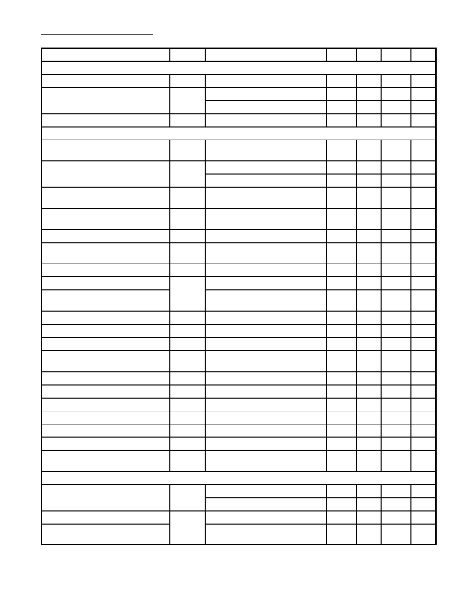
Electrical Characteristics: (V
P
= 17.5V, T
A
= +25
¯
C, V
FB
= 45V, f
i
= 50Hz, I
I(sb)
= 400
ç
A
unless otherwise specified)
Parameter
Symbol
Test Conditions
Min
Typ
Max
Unit
DC Supply
Operating Supply Voltage
V
P
9
Ù
25
V
Flyback Supply Voltage
V
FB
V
P
Ù
50
V
Note 1
V
P
Ù
60
V
Supply Current
I
P
No Load, No Signal
Ù
30
55
mA
Vertical Circuit
Output Voltage Swing (Scan)
V
O
I
diff
= 0.6mA
(PÙP)
, V
diff
= 1.8V
(PÙP)
,
I
O
= 3A
(PÙP)
19.8
Ù
Ù
V
Linearity Error
LE
I
O
= 3A
(PÙP)
, Note 4
Ù
1
3
%
I
O
= 50mA
(PÙP)
, Note 4
Ù
1
3
%
Output Voltage Swing (Flyback)
V
O(A)
Ù V
O(B)
V
O
I
diff
= 0.3mA, I
O
= 1.5A
Ù
39
Ù
V
Forward Voltage of the Internal
Efficiency Diode (V
O(A)
Ù V
FB
)
V
DF
I
O
= Ù1.5A, I
diff
= 0.3mA
Ù
Ù
1.5
V
Output Offset Current
|I
OS
|
I
diff
= 0, I
I(sb)
= 50
ç
A to 500
ç
A
Ù
Ù
30
mA
Offset Voltage at the Input of the
Feedback Amplifier (V
I(fb)
Ù V
O(B)
)
V
OS
T
I
diff
= 0
Ù
Ù
72
ç
V/K
DC Output Voltage
V
O(A)
I
diff
= 0, Note 5
Ù
8
Ù
V
Open Loop Voltage Gain (V
7Ù4
/V
1Ù2
)
G
VO
Note 6, Note 7
Ù
80
Ù
dB
Open Loop Voltage Gain
(V
7Ù4
/V
9Ù4
, V
1Ù2
= 0)
Note 6
Ù
80
Ù
dB
Voltage Ratio V
1Ù2
/V
9Ù4
V
R
Ù
0
Ù
dB
Frequency Response (Ù3dB)
f
res
Open Loop, Note 8
Ù
40
Ù
Hz
Current Gain (I
O
/I
diff
)
G
I
Ù
5000
Ù
Current Gain Drift as a Function
of Temperature
G
C
T
Ù
Ù
10
Ù4
K
Signal Bias Current
I
I(sb)
50
400
500
ç
A
Flyback Supply Current
I
FB
During Scan
Ù
Ù
100
ç
A
Power Supply Ripple Rejection
PSRR
Note 9
Ù
80
Ù
dB
DC Input Voltage
V
I(DC)
Ù
2.7
Ù
V
Common Mode Input Voltage
V
I(CM)
I
I(sb)
= 0
0
Ù
1.6
V
Input Bias Current
I
bias
I
I(sb)
= 0
Ù
0.1
0.5
ç
A
Common Mode Output Current
I
O(CM)
I
I(sub)
= 300
ç
A
(PÙP)
, f
i
= 50Hz,
I
diff
= 0
Ù
0.2
Ù
mA
Guard Circuit
Output Current
I
O
Not Active, V
O(guard)
= 0V
Ù
Ù
50
ç
A
Active, V
O(guard)
= 3.6V
1.0
Ù
2.5
mA
Output Voltage on Pin8
V
O(guard)
I
O
= 100
ç
A
4.6
Ù
5.5
V
Allowable Voltage on Pin8
Maximum Leakage Current =
10
ç
A
Ù
Ù
40
V
Notes:
Note 1. A flyback supply voltage of > 50V up to 60V is allowed in application. A 22ÙnF capacititor
in series with a 22
resistor (depending on I
O
and the inductance of the coil) has to be con-
nected between Pin7 and GND. The decoupling capacitor of V
FB
has to be connected be-
tween Pin6 and Pin3. This supply voltage line must have a resistance of 33
.
Note 4. The linearity error is measured without SÙcorrection and based on the same measurement
principle as performed on the screen. The measuring method is as follows:
Divide the output signal I
4
Ù I
7
(V
RM
) into 22 equal parts ranging from 1 to 22 inclusive. Measure
the value of two succeeding parts called one block starting with part 2 and 3 (block 1) and ending
with part 20 and 21 (block 10). Thus part 1 and 22 are unused. The equations for linearity error
for adjacent blocks (LEAB) and linearity error for not adjacent blocks (LENAB) are given below:
LEAB =
a
k
Ù a
(k + 1)
a
avg
; LEAB =
a
max
Ù a
min
a
avg
Note 5. Referenced to V
P
.
Note 6. The V values within formulae relate to voltages at or across relative pin numbers, i.e.
V
7Ù4
/V
1Ù2
= voltage value across Pin7 and Pin4 divided by voltage value across Pin1 and Pin2.
Note 7. V
9Ù4
AC shortÙcircuited.
Note 8. Frequency response V
7Ù4
/V
9Ù4
is equal to frequency response V
7Ù4
/V
1Ù2
.
Note 9. At V
(ripple)
= 500mV eff; measured across R
M
; f
i
= 50Hz.
I
drive(pos)
I
drive(neg)
V
O(B)
V
FB
V
O(A)
V
O(guard)
V
I(fb)
V
P
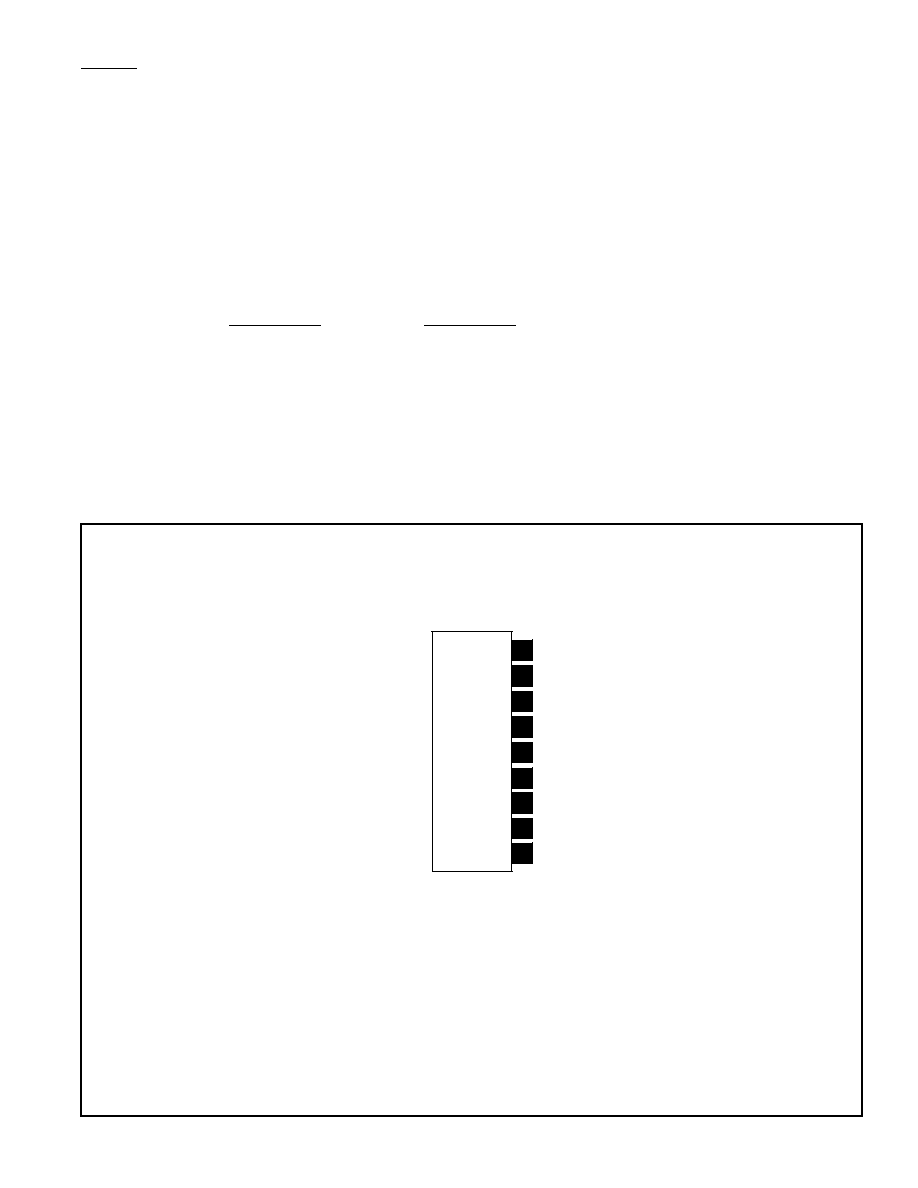
Pin Connection Diagram
(Front View)
GND
9
8
7
6
5
4
3
2
1
