NTE871
Integrated Circuit
Wideband High Speed Operational Amp
Description:
The NTE871 is a large≠signal wideband, high speed operational amplifier which has a unity gain
crossover frequency (f
T
) of approximately 38MHz and an open≠loop, 3dB corner frequency of approx-
imately 110kHz. It can operate at a total supply voltage of from 14 to 36 volts (
±
7 to
±
18 votls when
using split supplies) and can provide at least 18V
P≠P
and 30mA
P≠P
at the output when operating from
±
15 volt supplies. The NTE871 can be compensated with a single external capacitor and has DC
offset adjust terminals for those applications requiring offset null.
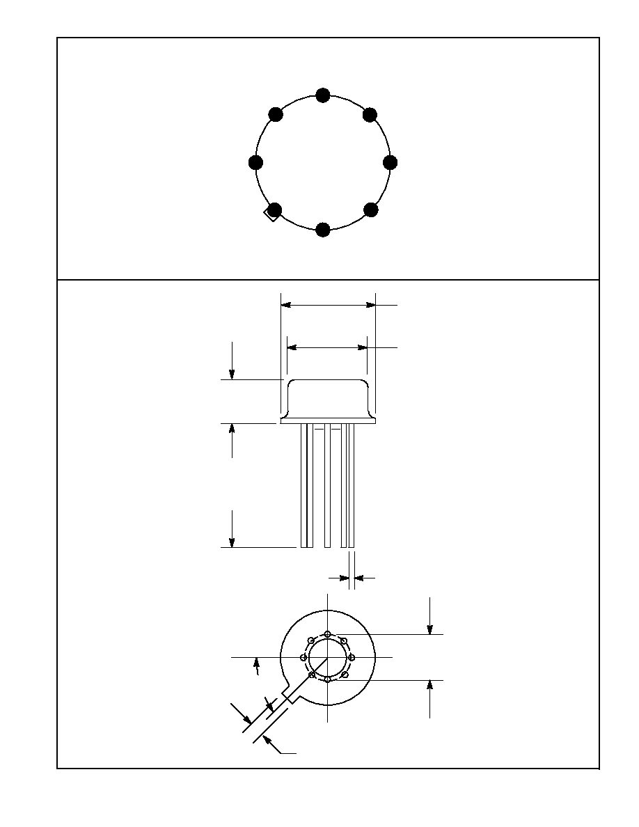
The NTE871 circuit contains both bipolar and PMOS transistors on a single monlithic chip and is sup-
plied in a 8≠Lead TO5 package.
Features:
D
High Open≠Loop Gain at Video Frequencies: 42dB Typ. at 1MHz
D
High Unity≠Gain Crossover Frequency: f
T
= 38MHz Typ.
D
Wide Power Bandwidth;
V
O
= 18V
P≠P
: 1.2MHz Typ.
D
High Slew Rate;
20dB Amplifier: 70V/
µ
s Typ.
Unity≠Gain Amplifier: 25V/
µ
s Typ.
D
Fast Setting Time: 0.6
µ
s Typ.
D
High Output Current:
±
15mA Min.
D
Single Capacitor Compensation
D
Offset Null Terminals
Absolute Maximum Ratings:
Supply Voltage (Between V+ and V≠ terminals)
36V
. . . . . . . . . . . . . . . . . . . . . . . . . . . . . . . . . . . . . . . .
Differential Input Voltage
±
12V
. . . . . . . . . . . . . . . . . . . . . . . . . . . . . . . . . . . . . . . . . . . . . . . . . . . . . . . . . . .
Input Voltage to GND (Note 1)
±
15V
. . . . . . . . . . . . . . . . . . . . . . . . . . . . . . . . . . . . . . . . . . . . . . . . . . . . . .
Offset Terminal to V≠ Terminal Voltage
±
0.5V
. . . . . . . . . . . . . . . . . . . . . . . . . . . . . . . . . . . . . . . . . . . . . .
Output Current (Note 2)
50mA
. . . . . . . . . . . . . . . . . . . . . . . . . . . . . . . . . . . . . . . . . . . . . . . . . . . . . . . . . . .
Device Dissipation (Up to T
A
= +55
∞
C), P
D
630mW
. . . . . . . . . . . . . . . . . . . . . . . . . . . . . . . . . . . . . . . . .
Derate Above T
A
= +55
∞
C
6.67mW/
∞
C
. . . . . . . . . . . . . . . . . . . . . . . . . . . . . . . . . . . . . . . . . . . . . .
Operating Temperature Range, T
opr
≠55
∞
to +125
∞
C
. . . . . . . . . . . . . . . . . . . . . . . . . . . . . . . . . . . . . . . .
Storage Temperature range. T
stg
≠65
∞
to +150
∞
C
. . . . . . . . . . . . . . . . . . . . . . . . . . . . . . . . . . . . . . . . . . .
Lead Temperature (During Soldering), T
L
At distance 1/16"
±
1/32" (1.59
±
0.79mm) from case for 10s max
+265
∞
C
. . . . . . . . . . . . . . . .
Note 1. If the supply voltage is less than
±
15 volts, the maximum input voltage to GND is equal to
the supply voltage.
Note 2. The NTE871 does not contain circuitry to protect against short circuits in the output.
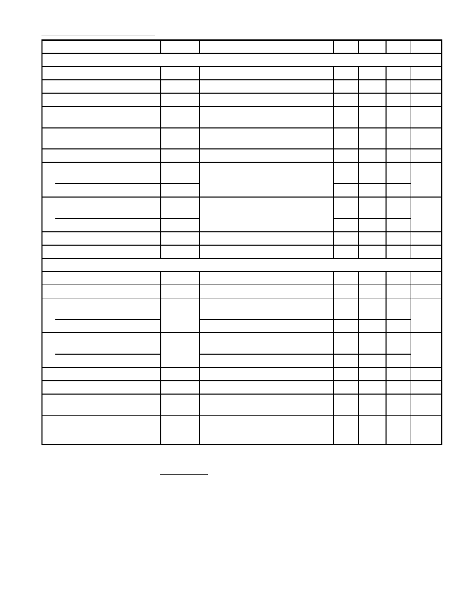
Electrical Characteristics: (T
A
= +25
∞
C, V
CC
=
±
15V unless otherwise specified)
Parameter
Symbol
Test Conditions
Min
Typ
Max
Unit
Static
Input Offset Voltage
V
IO
V
O
= 0
±
0.1V
≠
±
1
±
5
mV
Input Bias Current
I
IB
V
O
= 0
±
0.1V
≠
0.7
2.0
µ
A
Input Offset Current
I
IO
V
O
= 0
±
0.1V
≠
±
0.05
±
0.4
µ
A
Low≠Frequency Open≠Loop
Voltage Gain
A
OL
V
O
=
±
1V Peak, F = 1kHz, Note 3
56
61
≠
dB
Common≠Mode Input Voltage
Range
V
ICR
CMRR
76dB
±
12
+14
≠13
≠
V
Common≠Mode Rejection Ratio
CMRR
V
I
Common Mode =
±
12V
76
90
≠
dB
Maximum Output Voltage:
Positive
V
OM
+
Differential Input Voltage = 0
±
0.1V
+9
+11
≠
V
Negative
V
OM
≠
R
L
= 2k
≠9
≠11
≠
Maximum Output Current:
Positive
V
OM
+
Differential Input Voltage = 0
±
0.1V
+15
+30
≠
mA
Negative
V
OM
≠
R
L
= 250k
≠15
≠30
≠
Supply Current
I+
V
O
= 0
±
0.1V, R
L
10k
≠
8.5
10.5
mA
Power Supply Rejection Ratio
PSRR
V+ =
±
1V,
V≠ =
±
1V
60
70
≠
dB
Dynamic
Unity≠Gain Crossover Frequency
f
T
C
C
= 0, V
O
= 0.3V
P≠P
≠
38
≠
MHz
1MHz Open≠Loop Voltage Gain
A
OL
f = 1MHz, C
C
= 0, V
O
= 10V
P≠P
36
42
≠
dB
Slew Rate
20dB Amplifier
SR
A
V
= 10, C
C
= 0, V
I
= 1V (Pulse)
50
70
≠
V/
µ
s
Follower Mode
A
V
= 1, C
C
= 10pF, V
I
= 10V (Pulse)
≠
25
≠
Power Bandwidth
20dB Amplifier
PBW
(Note 4)
A
V
= 10, C
C
= 0, V
O
= 10V
P≠P
0.8
1.2
≠
MHz
Follower Mode
A
V
= 1, C
C
= 10pF, V
O
= 10V
P≠P
≠
0.4
≠
Open≠Loop Differential Impedance
Z
I
F = 1MHz
≠
30
≠
k
Open≠Loop Output Impedance
Z
O
F = 1MHz
≠
110
≠
Wideband Noise Voltage
Referred to Input
e
N
(Total)
BW = 1MHz, R
S
= 1k
≠
8
≠
µ
V
RMS
Setting Time
(To Within
±
50mV of 9V
Output Swing)
t
s
R
L
= 2k
, C
L
= 20pF
≠
0.6
≠
µ
s
Note 3. Low≠frequency dynamic characteristics.
Note 4. Power Bandwidth =
Slew Rate
V
O
(P≠P)