NTE2383
MOSFET
P≠Channel Enhancement Mode,
High Speed Switch
(Compl to NTE2382)
Description:
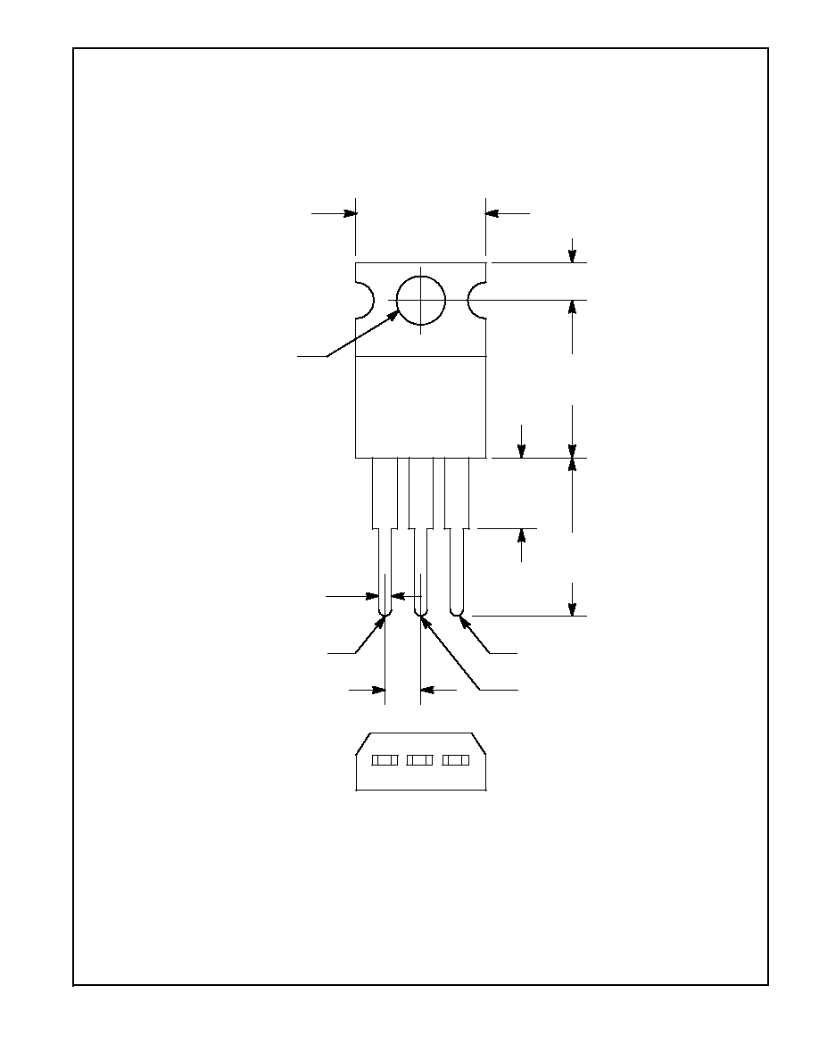
The NTE2383 is a MOS power P≠Channel FET in a TO220 type package designed for high voltage,
high speed power switching applications such as switching regulators, converters, solenoid, and relay
drivers.
Features:
D
Lower R
DS(ON)
D
Improved Inductive Ruggedness
D
Fast Switching Times
D
Rugged Polysilicon Gate Cell Structure
D
Lower Input Capacitance
D
Extended Safe Operating Area
D
Improved High Temperature Reliability
Absolute Maximim Ratings:
Drain≠Source Voltage (Note 1), V
DSS
100V
. . . . . . . . . . . . . . . . . . . . . . . . . . . . . . . . . . . . . . . . . . . . . . . .
Drain≠Gate Voltage (R
GS
= 1M
, Note 1), V
DGR
100V
. . . . . . . . . . . . . . . . . . . . . . . . . . . . . . . . . . . . . .
Gate≠Source Voltage, V
GS
±
20V
. . . . . . . . . . . . . . . . . . . . . . . . . . . . . . . . . . . . . . . . . . . . . . . . . . . . . . . . .
Continuous Drain Current, I
D
T
C
= +25
∞
C
10.5A
. . . . . . . . . . . . . . . . . . . . . . . . . . . . . . . . . . . . . . . . . . . . . . . . . . . . . . . . . . . . . . . .
T
C
= +100
∞
C
7.5A
. . . . . . . . . . . . . . . . . . . . . . . . . . . . . . . . . . . . . . . . . . . . . . . . . . . . . . . . . . . . . . . .
Drain Current, Pulsed (Note 3), I
DM
42A
. . . . . . . . . . . . . . . . . . . . . . . . . . . . . . . . . . . . . . . . . . . . . . . . . . .
Gate Current, Pulsed, I
GM
±
1.5A
. . . . . . . . . . . . . . . . . . . . . . . . . . . . . . . . . . . . . . . . . . . . . . . . . . . . . . . . .
Single Pulsed Avalanvhe Energy (Note 4), E
AS
510mJ
. . . . . . . . . . . . . . . . . . . . . . . . . . . . . . . . . . . . . .
Avalanche Current, I
AS
10.5A
. . . . . . . . . . . . . . . . . . . . . . . . . . . . . . . . . . . . . . . . . . . . . . . . . . . . . . . . . . . .
Total Power Dissipation (T
C
= +25
∞
C), P
D
75W
. . . . . . . . . . . . . . . . . . . . . . . . . . . . . . . . . . . . . . . . . . . .
Derate Above 25
∞
C
0.6W/
∞
C
. . . . . . . . . . . . . . . . . . . . . . . . . . . . . . . . . . . . . . . . . . . . . . . . . . . . . . .
Operating Junction Temperature Range, T
opr
≠55
∞
to +150
∞
C
. . . . . . . . . . . . . . . . . . . . . . . . . . . . . . . .
Storage Temperature Range, T
stg
≠55
∞
to +150
∞
C
. . . . . . . . . . . . . . . . . . . . . . . . . . . . . . . . . . . . . . . . . .
Thermal Resistance, Junction≠to≠Ambient, R
thJA
62.5
∞
C/W
. . . . . . . . . . . . . . . . . . . . . . . . . . . . . . . . . .
Thermal Resistance, Junction≠to≠Case, R
thJC
1.67
∞
C/W
. . . . . . . . . . . . . . . . . . . . . . . . . . . . . . . . . . . .
Thermal Resistance, Case≠to≠Sink (Note 5), R
thCS
0.5
∞
C/W
. . . . . . . . . . . . . . . . . . . . . . . . . . . . . . . . .
Maximum Lead Temperature (During Soldering, 1/8" from case, 5sec), T
L
+300
∞
C
. . . . . . . . . . . . . .
Note 1. T
J
= +25
∞
to +150
∞
C
Note 2. Pulse Test: Pulse Width
300
µ
s, Duty Cycle
2%.
Note 3. Repetitive rating: Pulse width limited by max. junction temperature.
Note 4. L = 8.5mH, V
DD
= 25V, R
G
= 25
, Starting T
J
= +25
∞
C.
Note 5. Mounting surface flat, smooth, and greased.

Electrical Characteristics: (T
C
= +25
∞
C unless otherwise specified)
Parameter
Symbol
Test Conditions
Min
Typ
Max
Unit
Drain≠Source Breakdown Voltage
V
(BR)DSS
V
GS
= 0, I
D
= 0.25mA
100
≠
≠
V
Zero Gate Voltage Drain Current
I
DSS
V
DS
= 100V, V
GS
= 0
≠
≠
0.25
mA
V
DS
= 80V, V
GS
= 0, T
J
= +125
∞
C
≠
≠
1.0
mA
Gate≠Body Leakage Current, Forward
I
GSS
V
GS
= 20V
≠
≠
100
nA
Gate≠Body Leakage Current, Reverse
I
GSS
V
GS
= 20V
≠
≠
≠100
nA
Gate Threshold Voltage
V
GS(th)
V
DS
= V
GS
, I
D
= 0.25mA
2.0
≠
4.0
V
Static Drain≠Source On≠Resistance
r
DS(on)
V
GS
= 10V, I
D
= 5.3A, Note 2
≠
≠
0.3
Forward Transconductance
g
FS
V
DS
50V, I
D
= 5.3A, Note 2
2.0
≠
≠
mhos
Input Capacitance
C
iss
V
DS
= 25V, V
GS
= 0, f = 1MHz
≠
835
≠
pF
Output Capacitance
C
oss
≠
357
≠
pF
Reverse Transfer Capacitance
C
rss
≠
94
≠
pF
Turn≠On Delay Time
t
d(on)
V
DD
= 50V, I
D
= 10.5A, Z
O
= 24
,
≠
≠
60
ns
Rise Time
t
r
MOSFET switching times are
essentially independent of operating
≠
≠
140
ns
Turn≠Off Delay Time
t
d(off)
essentially independent of operating
temperature
≠
≠
140
ns
Fall Time
t
f
≠
≠
140
ns
Total Gate Charge
Q
g
V
GS
= 10V, V
DS
= 80V, I
D
= 10.5A,
≠
≠
58
nC
Gate≠Source Charge
Q
gs
Gate charge is essentially
independent of operating
≠
12.6
≠
nC
Gate≠Drain ("Miller") Charge
Q
gd
independent of operating
temperature
≠
16.6
≠
ns
Source≠Drain Diode Ratings and Characteristics
Continuous Source Current
(Body Diode)
I
S
≠
≠
10.5
A
Pulse Source Current (Body Diode)
I
SM
Note 3
≠
≠
42
A
Diode Forward Voltage
V
SD
T
J
= +25
∞
C, I
S
= 10.5A, V
GS
= 0V,
Note 2
≠
≠
6.3
V
Reverse Recovery Time
t
rr
T
J
= +25
∞
C, I
F
= 10.5A,
dI
F
/dt = 100A/
µ
s
≠
≠
300
ns
Note 2. Pulse Test: Pulse Width
300
µ
s, Duty Cycle
2%.
Note 3. Repetitive rating: Pulse width limited by max. junction temperature.