 | –≠–ª–µ–∫—Ç—Ä–æ–Ω–Ω—ã–π –∫–æ–º–ø–æ–Ω–µ–Ω—Ç: NTE927 | –°–∫–∞—á–∞—Ç—å:  PDF PDF  ZIP ZIP |
NTE2057
Integrated Circuit
Dual 16≠Bit Digital≠to≠Analog Converter
for CD and DAT Players
Description:
The NTE2057 is a monolithic integrated dual 16≠bit digital ≠to≠analog converter (DAC) in a 28≠Lead
DIP type package designed for use in Hi≠Fi digital audio equipment such as compact disc players,
digital tape, or cassette recorders.
Features:
D
Selectable Input Format: Offset Binary or Two's Complement
D
Internal Timing and Control Circuit
D
TTL≠Compatible Digital Inputs
D
High Maximum Input Bit Rate and Fast Settling Time
D
6Mbits/s Data Rate
D
Low Linearity Error (1/2 LSB typ)
D
Fast Settling (1
µ
s typ)
Applications:
D
Compact Disc Players
D
Digital Audio Tape, and Cassette Recorders and Players
D
Waveform Generation
Absolute Maximum Ratings:
Supply Voltage Range, V
DD
Pin28 (V
DD
)
+7V
. . . . . . . . . . . . . . . . . . . . . . . . . . . . . . . . . . . . . . . . . . . . . . . . . . . . . . . . . . . . . . . . .
Pin26 (V
DD1
)
≠7V
. . . . . . . . . . . . . . . . . . . . . . . . . . . . . . . . . . . . . . . . . . . . . . . . . . . . . . . . . . . . . . . .
Pin15 (V
DD2
)
≠17V
. . . . . . . . . . . . . . . . . . . . . . . . . . . . . . . . . . . . . . . . . . . . . . . . . . . . . . . . . . . . . . .
Junction Temperature Range, T
J
≠55
∞
to +150
∞
C
. . . . . . . . . . . . . . . . . . . . . . . . . . . . . . . . . . . . . . . . . . .
Operating Ambient Temperature Range, T
A
≠20
∞
to +70
∞
C
. . . . . . . . . . . . . . . . . . . . . . . . . . . . . . . . . . .
Storage Temperature Range, T
stg
≠65
∞
to +150
∞
C
. . . . . . . . . . . . . . . . . . . . . . . . . . . . . . . . . . . . . . . . . .
Electrostatic Handling (Note 1), V
ES
≠1000 to +1000V
. . . . . . . . . . . . . . . . . . . . . . . . . . . . . . . . . . . . . .
Note 1. Discharging a 250pF capacitor through a 1k
series resistor.
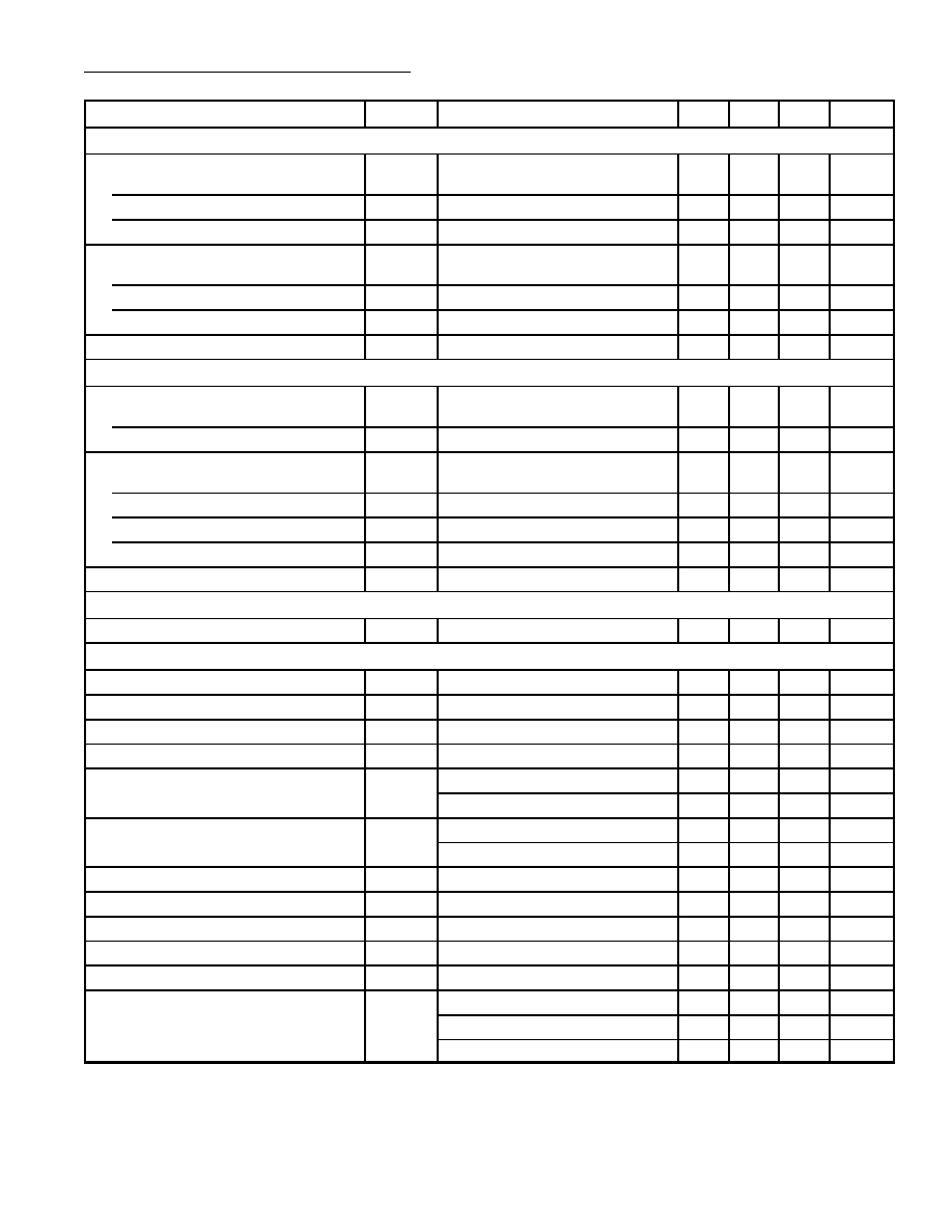
DC and AC Electrical Characteristics: (V
DD
= +5V, V
DD1
= ≠5V, V
DD2
= ≠15V, T
A
= +25
∞
C
unless otherwise specified)
Parameter
Symbol
Test Conditions
Min
Typ
Max
Unit
Supply
Supply Voltage Range
Pin28
V
DD
4.0
5.0
6.0
V
Pin26
≠V
DD1
4.5
5.0
6.0
V
Pin15
≠V
DD2
14.0
15.0
16.0
V
Supply Currents
Pin28
I
DD
≠
45
60
mA
Pin26
≠I
DD1
≠
45
75
mA
Pin15
≠I
DD2
≠
25
60
mA
Resolution
≠
16
≠
bits
Inputs
Input Current (Pin3, Pin4)
Digital Inputs Low
I
IL
< 0.8V
≠
≠
TBD
mA
Digital Inputs High
I
IH
> 2.0V
≠
≠
TBD
µ
A
Input Frequency
At Clock Input (Pin4)
f
SCK
≠
≠
6
MHz
At Clock Input (Pin2)
f
BCK
≠
≠
≠
MHz
At Data Inputs (Pin3, Pin4)
f
DAT
≠
≠
≠
MHz
At Word Select Input (Pin1)
f
WS
≠
≠
≠
kHz
Input Capacitance of Digital Inputs
C
I
≠
12
≠
pF
Oscillator
Oscillator Frequency
w
/Internal Capacitor
f
OSC
150
200
250
kHz
Analog Outputs (AOL, AOR)
Output Voltage Compliance
V
CC
TBD
≠
TBD
mV
Full≠Scale Current
I
FS
3.4
4.0
4.6
mA
Zero≠Scale Current
±
I
ZS
≠
TBD
≠
nA
Full≠Scale Temperature Coefficient
TC
FS
T
A
= ≠20
∞
to +70
∞
C
≠
±
200
≠
ppm/
∞
C
Linearity Error Integral
E
1
T
A
= +25
∞
C
≠
0.5
≠
LSB
T
A
= ≠20
∞
to +70
∞
C
≠
TBD
≠
LSB
Linearity Error Differential
E
D1
T
A
= +25
∞
C
≠
0.5
1.0
LSB
T
A
= ≠20
∞
to +70
∞
C
≠
TBD
≠
LSB
Signal≠to≠Noise Ratio + THD
S/N
Note 2
90
95
≠
dB
Setting Time to
±
1 LSB
t
CS
≠
1
≠
µ
s
Channel Separation
T
80
TBD
≠
dB
Unbalance Between Outputs
I
FS
≠
0.1
0.2
dB
Time Delay Between Outputs
t
D
≠
≠
1
µ
s
Power Supply Ripple Rejection (Note 3)
RR
V
DD
= +5V
≠
TBD
≠
dB
V
DD1
= ≠5V
≠
TBD
≠
dB
V
DD2
= ≠15V
≠
TBD
≠
dB
Note 2. Signal≠to≠noise ratio + THD with 1kHz full≠scale sine wave generated at a sampling rate
of 176.4kHz.
Note 3. V
RIPPLE
= 1% of supply voltage and f
RIPPLE
= 100Hz.
DC and AC Electrical Characteristics (Cont'd): (V
DD
= +5V, V
DD1
= ≠5V, V
DD2
= ≠15V,
T
A
= +25
∞
Cunless otherwise specified)
Parameter
Symbol
Test Conditions
Min
Typ
Max
Unit
Analog Outputs (AOL, AOR) (Cont'd)
Signal≠to≠Noise Ratio at Bipolar Zero
S/N
≠
≠100
≠
dB
Timing
Rise Time
t
R
≠
≠
35
ns
Fall Time
t
F
≠
≠
35
ns
Bit Clock Cycle Time
t
CY
160
≠
≠
ns
Bit Clock High Time
t
HB
48
≠
≠
ns
Bit Clock Low Time
t
LB
48
≠
≠
ns
Bit Clock Fall Time to Latch Rise Time
t
FBRL
0
≠
≠
ns
Bit Clock Rise Time to Latch Fall Time
t
RBFL
0
≠
≠
ns
Data Setup Time to Bit Clock
t
SDB
32
≠
≠
ns
Data Hold Time to Bit Clock
t
HDB
0
≠
≠
ns
Data Setup Time to System Clock
t
SDS
32
≠
≠
ns
Word Select Hold Time to System Clock
t
HWS
0
≠
≠
ns
Word Select Setup Time to System Clock
t
SWS
32
≠
≠
ns
Bit Clock Fall Time to System Clock Rise Time
t
FBRS
32
≠
≠
ns
System Clock Rise Time to Bit Clock Fall Time
t
RSFB
32
≠
≠
ns
System Clock Fall Time to Bit Clock Rise Time
t
FSRB
50
≠
≠
ns
Bit Clock Rise Time to System Clock Fall Time
t
RBFS
0
≠
≠
ns
Latch Enable Low Time
t
LLE
20
≠
≠
ns
Latch Enable High Time
t
HLE
32
≠
≠
ns
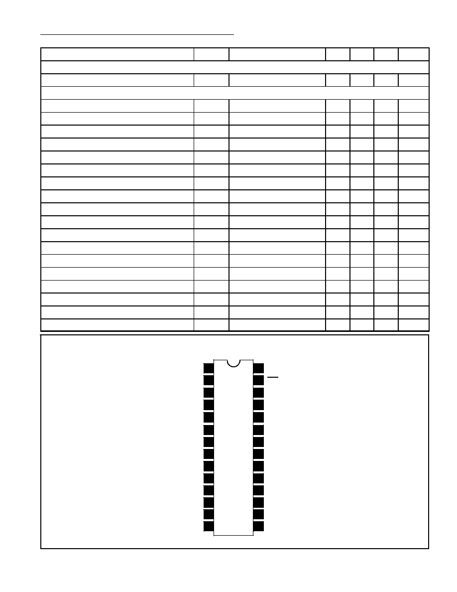
V
DD
2
C
CLK
C
CLK
V
DD
1
OB/TWC
V
DD
D
GND
A
GND
Pin Connection Diagram
AOL
LE/WS
Decoupling
Data R/SCK
Decoupling
Decoupling
Decoupling
Decoupling
Decoupling
Decoupling
Decoupling
1
2
3
4
BCK
Data l/Data
5
6
AOR
7
Decoupling
8
28
27
26
25
24
23
22
21
9
Decoupling
20
Decoupling
Decoupling
10
Decoupling
11
19
18
12
17
13
Decoupling
16
14
15

1.469 (37.32) Max
1.300 (33.02)
.540
(13.7)
.600
(15.24)
.250
(6.35)
.122
(3.1)
Min
.100 (2.54)
15
28
14
1