NTE937M
Integrated Circuit
JFET Input Operational Amplifier
Description:
The NTE937M is a monolithic JFET input operational amplifier in an 8≠Lead DIP type package incor-
porating well≠matched, high voltage JFET's on the same chip with standard bi≠polar transistors. This
amplifier features low input bias and offset currents, low offset voltage and offset voltage drift, coupled
with offset adjust which does not degrade drift or common≠mode rejection. It is also designed for high
slew rate, wide bandwidth, extremely fast settling time, low voltage and current noise and a low 1/f
noise corner.
Advantages:
D
Replaces Expensive Hybrid and Module FET OP Amps
D
Rugged JFET's Allow Blow≠Out Free Handling Compared with MOSFET Input Device
D
Excellent for Low Noise Applications using either High or Low Source Impedance ≠ Very Low
1/f Corner
D
Offset Adjust does not Degrade Drift or Common≠Mode Rejection as in Most Monolithic Amplifiers
D
New Output Stage Allows use of Large Capacitive Loads (10,000pF) without Stability Problems
D
Internal Compensation and Large Differential Input Voltage Capability
Applications:
D
Precision High Speed Integrators
D
Fast D/A and A/D Converters
D
High Impedance Buffers
D
Wideband, Low Noise, Low Drift Amplifiers
D
Logarithmic Amplifiers
D
Photocell Amplifiers
D
Sample and Hold Circuits
Absolute Maximum Ratings:
Supply Voltage
±
18V
. . . . . . . . . . . . . . . . . . . . . . . . . . . . . . . . . . . . . . . . . . . . . . . . . . . . . . . . . . . . . . . . . . . .
Maximum Power Dissipation (at +25
∞
C, Note 1), P
d
500mW
. . . . . . . . . . . . . . . . . . . . . . . . . . . . . . . . .
Differential Input Voltage
±
30V
. . . . . . . . . . . . . . . . . . . . . . . . . . . . . . . . . . . . . . . . . . . . . . . . . . . . . . . . . . .
Input Voltage Range (Note 2)
±
16V
. . . . . . . . . . . . . . . . . . . . . . . . . . . . . . . . . . . . . . . . . . . . . . . . . . . . . . .
Output Short≠Circuit Duration
Continuous
. . . . . . . . . . . . . . . . . . . . . . . . . . . . . . . . . . . . . . . . . . . . . . . . .
Maximum Operating Junction Temperature (Note 1), T
J
max
+100
∞
C
. . . . . . . . . . . . . . . . . . . . . . . . . .
Storage Temperature Range, T
stg
≠65
∞
to +150
∞
C
. . . . . . . . . . . . . . . . . . . . . . . . . . . . . . . . . . . . . . . . . .
Lead Temperature (During Soldering, 10sec), T
L
+300
∞
C
. . . . . . . . . . . . . . . . . . . . . . . . . . . . . . . . . . . .
Thermal Resistance, Junction≠to≠Ambient (Note 1), R
thJC
+155
∞
C/W
. . . . . . . . . . . . . . . . . . . . . . . . .
Note 1. The maximum power dissipation for this device must be derated at elevated temperatures
and is dictated by T
J
max, R
thJC
, and the ambient temperature, T
A
. The maximum available
power dissipation at any temperature is P
d
= (T
J
max ≠ T
A
)/R
thJC
or the +25
∞
C P
d
max, which-
ever is less.
Note 2. Unless otherwise specified, the absolute maximum negative input voltage is equal to the
negative power supply voltage.
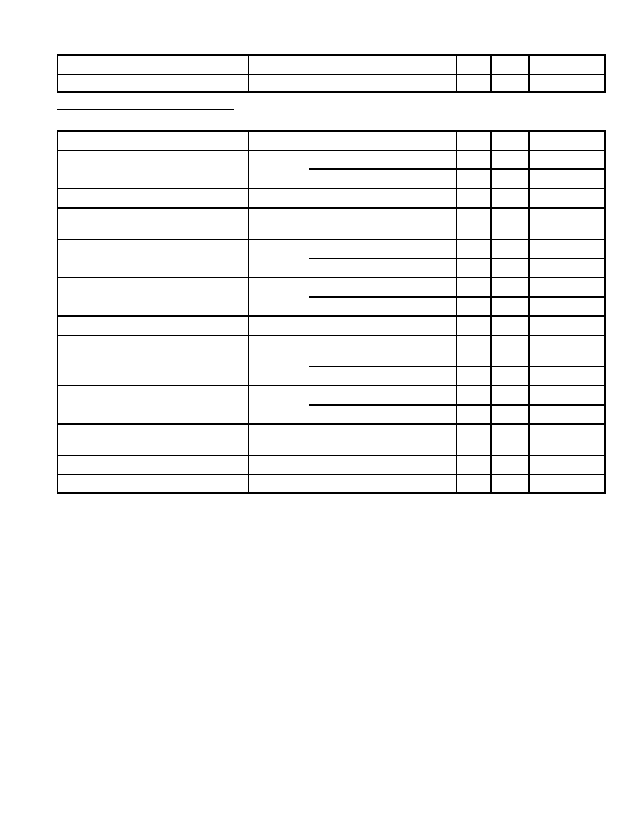
DC Electrical Characteristics: (T
A
= +25C, V
S
=
±
15V unless otherwise specified)
Parameter
Symbol
Test Conditions
Min
Typ
Max
Unit
Supply Current
I
CC
≠
5
10
mA
DC Electrical Characteristics: (V
S
=
±
15V, 0
∞
T
A
+70
∞
C, T
HIGH
= +70
∞
C unles otherwise
specified)
Parameter
Symbol
Test Conditions
Min
Typ
Max
Unit
Input Offset Voltage
V
OS
R
S
= 50
, T
A
= +25
∞
C
≠
3
10
mV
Over Temperature
≠
≠
13
mV
Average TC of Input Offset Voltage
V
OS
/
T
R
S
= 50
≠
5
≠
µ
V/
∞
C
Change in Average TC with V
OS
Adjust
TC/
V
OS
R
S
= 50
, Note 3
≠
0.5
≠
µ
V/
∞
C
Input Offset Current
I
OS
T
J
= +25
∞
C, Note 4
≠
3
50
pA
T
J
T
HIGH
≠
≠
2
nA
Input Bias Current
I
B
T
J
= +25
∞
C, Note 4
≠
30
200
pA
T
J
T
HIGH
≠
≠
8
nA
Input Resistance
R
IN
T
J
= +25
∞
C
≠
10
12
≠
Large Signal Voltage Gain
A
VOL
T
A
= +25
∞
C, V
O
=
±
10V,
R
L
= 2k
25
200
≠
V/mV
Over Temperature
15
≠
≠
V/mV
Output Voltage Swing
V
O
R
L
= 10k
±
12
±
13
≠
V
R
L
= 2k
±
10
±
12
≠
V
Input Common≠Mode Voltage Range
V
CM
±
10
+15.1
≠12
≠
V
Common≠Mode Rejection Ratio
CMRR
≠
80
100
dB
Supply Voltage Rejection Ratio
PSRR
Note 5
≠
80
100
dB
Note 3. The temperature coeficient of the adjust input offset voltage changes only a small amount
(0.5
µ
V/
∞
C typically) for each mV of adjustment from its original unadjusted value. Common≠
mode rejection and open loop voltage gain are also unaffected by offset adjustment.
Note 4. The input bias currents are junction leakage currents which approximately double for every
10
∞
C increase in the junction temperature, T
J
. Due to limited production test time, the input
bias currents measured are correlated to junction temperature. In normal operation the junc-
tion temperature rises above the ambient temperature as a result of internal power dissipa-
tion, P
d
. T
J
= T
A
+ R
thJC
P
d
where R
thJC
is the thermal resistance from junction to ambient.
Use of a heat sink is recommended if input bias current is to be kept to a minimum.
Note 5. Supply Voltage Rejection is measured for both supply magnitudes increasing or decreasing
simultaneously, in accordance with common practice.
