 | –≠–ª–µ–∫—Ç—Ä–æ–Ω–Ω—ã–π –∫–æ–º–ø–æ–Ω–µ–Ω—Ç: NTE955 | –°–∫–∞—á–∞—Ç—å:  PDF PDF  ZIP ZIP |

NTE955MC
Integrated Circuit
CMOS Timing Circuit
Description:
The NTE955MC is a monolithic timing circuit in an 8≠Lead DIP type package fabricated using CMOS
process. This timer is fully compatible with CMOS, TTL, and MOS logic and operates at frequencies
up to 2MHz. Because of its high impedance, this device uses smaller timing capacitors than those
used by the NE555. As a result, more accurate time delays and oscillations are possible. Power con-
sumption is low across the full range of power supply voltage.
Like the NE555, the NTE955MC has a trigger level equal to approximately one≠third of the supply
voltage and a threshold level equal to approximately two≠thirds of the supply voltage. These levels
can be altered by use of the control voltage terminal (Pin5). When the trigger input (Pin2) falls below
the trigger level, the flip≠flop is set and the output goes high. If Pin2 is above the trigger level and the
threshold input (Pin6) is above the threshold level, the flip≠flop is reset and the output is low. The reset
input (Pin4) can override all other inputs and can be used to initiate a new timing cycle. If Pin4 is low,
the flip≠flop is reset and the output is low. Whenever the output is low, a low≠impedance path is pro-
vided between the discharge terminal (Pin7) and GND. All unused inputs should be tied to an ap-
propriate logic level to prevent false triggering.
While the CMOS output is capable of sinking over 100mA and sourcing over 10mA, the NTE955MC
exhibits greatly reduced supply≠current spikes during output transitions. This minimizes the need for
the large decoupling capacitors required by the NE555.
Features:
D
Direct Replacement for 555 Timers
D
Very Low Power Consumption: 1mW Typ at V
DD
= 5V
D
Operates in Both Astable and Monostable Modes
D
CMOS Output Capable of Swinging Rail to Rail
D
High Output Current Capability:
Sink 100mA Typ
Source 10mA Typ
D
Output Fully Compatible with CMOS, TTL, and MOS
D
Low Supply Current Reduces Spikes During Output Transitions
D
Single Supply Operation from 2V to 15V
Applications:
D
Precision Timing
D
Pulse Generation
D
Sequential Timing
D
Time Delay Generation
D
Pulse Width Modulation
D
Pulse Position Modulation
D
Linear Ramp Generator

Absolute Maximum Ratings: (T
A
= +25
∞
C, Note 1 unless otherwise specified)
Power Supply Voltage (Note 2), V
DD
18V
. . . . . . . . . . . . . . . . . . . . . . . . . . . . . . . . . . . . . . . . . . . . . . . . . .
Input Voltage Range (Any Input), V
I
≠0.3 to V
DD
. . . . . . . . . . . . . . . . . . . . . . . . . . . . . . . . . . . . . . . . . . . .
Sink Current, Discharge or Output
150mA
. . . . . . . . . . . . . . . . . . . . . . . . . . . . . . . . . . . . . . . . . . . . . . . . .
Source Current, Output, I
O
15mA
. . . . . . . . . . . . . . . . . . . . . . . . . . . . . . . . . . . . . . . . . . . . . . . . . . . . . . . .
Continuous Total Power Dissipation, P
D
1000mW
. . . . . . . . . . . . . . . . . . . . . . . . . . . . . . . . . . . . . . . . . .
Derate Above 25
∞
C
8mW/
∞
C
. . . . . . . . . . . . . . . . . . . . . . . . . . . . . . . . . . . . . . . . . . . . . . . . . . . . . . .
Operating Temperature Range, T
A
0
∞
to +70
∞
C
. . . . . . . . . . . . . . . . . . . . . . . . . . . . . . . . . . . . . . . . . . . . .
Storage Temperature Range, T
stg
≠65
∞
to +150
∞
C
. . . . . . . . . . . . . . . . . . . . . . . . . . . . . . . . . . . . . . . . . .
Lead Temperature (During Soldering, 10sec), T
L
+260
∞
C
. . . . . . . . . . . . . . . . . . . . . . . . . . . . . . . . . . . .
Note 1. Stresses beyond those listed under "Absolute Maximum Ratings" may cause permanent
damage to the device. These are stress ratings only and functional operation of the device
at these or any other conditions beyond those indicated under "Recommended Operating
Conditions" is not implied. Exposure to absolute≠maximum≠rated conditions for extended
periods may affect device reliability.
Note 2. All voltage values are with respect to network GND.
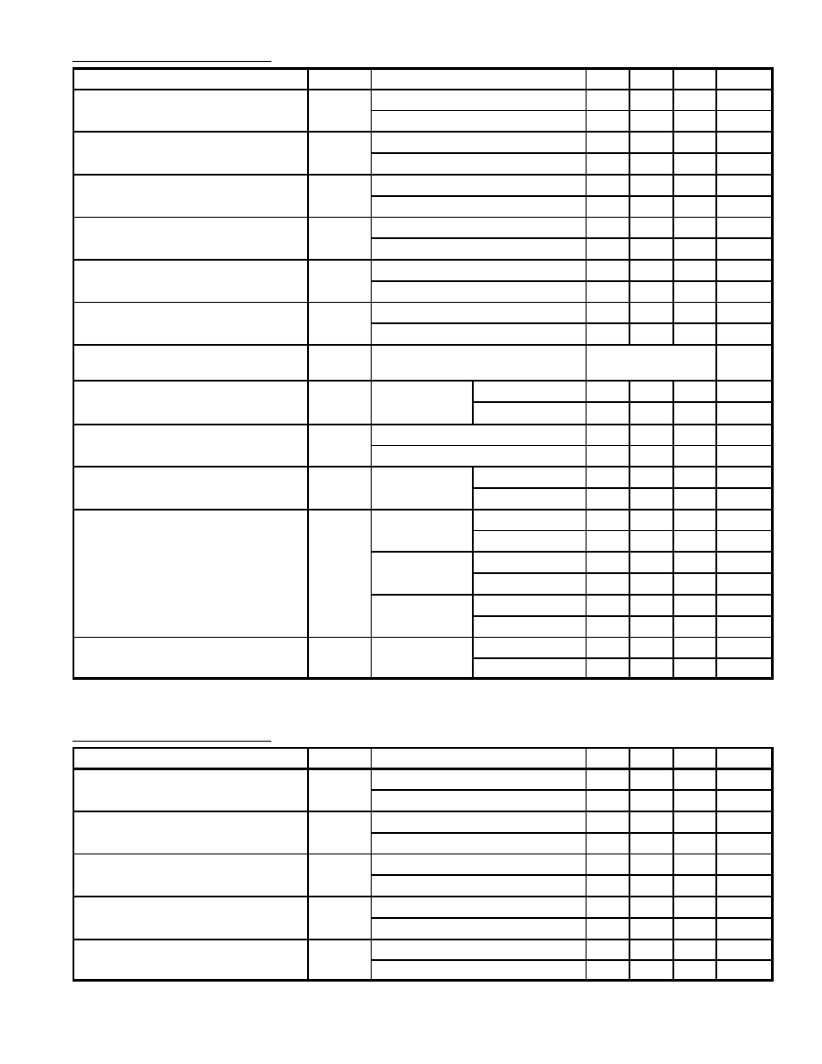
Recommended Operating Conditions:
Parameter
Symbol
Test Conditions
Min
Typ
Max
Unit
Supply Voltage
V
DD
2
≠
15
V
Operating Ambient Temperature Range
T
A
0
≠
70
∞
C
Electrical Characteristics: (T
A
= +25
∞
C, V
DD
= 2V unless otherwise specified)
Parameter
Symbol
Test Conditions
Min
Typ
Max
Unit
Threshold Voltage
V
TH
0.95
1.33
1.65
V
T
A
= 0
∞
to +70
∞
C
0.85
≠
1.75
V
Threshold Current
I
TH
≠
10
≠
pA
T
A
= 0
∞
to +70
∞
C
≠
75
≠
pA
Trigger Voltage
V
T
0.4
0.67
0.95
V
T
A
= 0
∞
to +70
∞
C
0.3
≠
1.05
V
Trigger Current
I
T
≠
10
≠
pA
T
A
= 0
∞
to +70
∞
C
≠
75
≠
pA
Reset Voltage
V
R
0.4
1.1
1.5
V
T
A
= 0
∞
to +70
∞
C
0.3
≠
2.0
V
Reset Current
I
R
≠
10
≠
pA
T
A
= 0
∞
to +70
∞
C
≠
75
≠
pA
Control Voltage (Open Circuit) as a
Percentage of Supply Voltage
T
A
= 0
∞
to +70
∞
C
66.7%
Discharge Switch On≠State Voltage
I
OL
= 1mA
≠
0.03
0.2
V
T
A
= 0
∞
to +70
∞
C
≠
≠
0.25
V
Discharge Switch Off≠State Current
≠
0.1
≠
nA
T
A
= 0
∞
to +70
∞
C
≠
0.5
≠
nA
High≠Level Output Voltage
V
OH
I
OH
= ≠300
µ
A
1.5
1.9
≠
V
T
A
= 0
∞
to +70
∞
C
1.5
≠
≠
V
Low≠Level Output Voltage
V
OL
I
OL
= 1mA
≠
0.07
0.3
V
T
A
= 0
∞
to +70
∞
C
≠
≠
0.35
V
Supply Current
I
DD
Note 3
≠
≠
250
µ
A
T
A
= 0
∞
to +70
∞
C
≠
≠
400
µ
A
Note 3. These values apply for the expected operating configurations in which Pin6 is connected
directly to Pin7 or Pin2.
Electrical Characteristics: (T
A
= +25
∞
C, V
DD
= 5V unless otherwise specified)
Parameter
Symbol
Test Conditions
Min
Typ
Max
Unit
Threshold Voltage
V
TH
2.8
3.3
3.8
V
T
A
= 0
∞
to +70
∞
C
2.7
≠
3.9
V
Threshold Current
I
TH
≠
10
≠
pA
T
A
= 0
∞
to +70
∞
C
≠
75
≠
pA
Trigger Voltage
V
T
1.36
1.66
1.96
V
T
A
= 0
∞
to +70
∞
C
1.26
≠
2.06
V
Trigger Current
I
T
≠
10
≠
pA
T
A
= 0
∞
to +70
∞
C
≠
75
≠
pA
Reset Voltage
V
R
0.4
1.1
1.5
V
T
A
= 0
∞
to +70
∞
C
0.3
≠
1.8
V
Reset Current
I
R
≠
10
≠
pA
T
A
= 0
∞
to +70
∞
C
≠
75
≠
pA
Control Voltage (Open Circuit) as a
Percentage of Supply Voltage
T
A
= 0
∞
to +70
∞
C
66.7%
Discharge Switch On≠State Voltage
I
OL
= 10mA
≠
0.14
0.5
V
T
A
= 0
∞
to +70
∞
C
≠
≠
0.6
V
Discharge Switch Off≠State Current
≠
0.1
≠
nA
T
A
= 0
∞
to +70
∞
C
≠
0.5
≠
nA
High≠Level Output Voltage
V
OH
I
OH
= ≠1mA
4.1
4.8
≠
V
T
A
= 0
∞
to +70
∞
C
4.1
≠
≠
V
Low≠Level Output Voltage
V
OL
I
OL
= 8mA
≠
0.21
0.4
V
T
A
= 0
∞
to +70
∞
C
≠
≠
0.5
V
I
OL
= 5mA
≠
0.13
0.3
V
T
A
= 0
∞
to +70
∞
C
≠
≠
0.4
V
I
OL
= 3.2mA
≠
0.08
0.3
V
T
A
= 0
∞
to +70
∞
C
≠
≠
0.35
V
Supply Current
I
DD
Note 3
≠
170
350
µ
A
T
A
= 0
∞
to +70
∞
C
≠
≠
500
µ
A
Note 3. These values apply for the expected operating configurations in which Pin6 is connected
directly to Pin7 or Pin2.
Electrical Characteristics: (T
A
= +25
∞
C, V
DD
= 15V unless otherwise specified)
Parameter
Symbol
Test Conditions
Min
Typ
Max
Unit
Threshold Voltage
V
TH
9.45
10.0
10.55
V
T
A
= 0
∞
to +70
∞
C
9.35
≠
10.65
V
Threshold Current
I
TH
≠
10
≠
pA
T
A
= 0
∞
to +70
∞
C
≠
75
≠
pA
Trigger Voltage
V
T
4.65
5.0
5.35
V
T
A
= 0
∞
to +70
∞
C
4.55
≠
5.45
V
Trigger Current
I
T
≠
10
≠
pA
T
A
= 0
∞
to +70
∞
C
≠
75
≠
pA
Reset Voltage
V
R
0.4
1.1
1.5
V
T
A
= 0
∞
to +70
∞
C
0.3
≠
1.8
V

Electrical Characteristics (Cont'd): (T
A
= +25
∞
C, V
DD
= 15V unless otherwise specified)
Parameter
Symbol
Test Conditions
Min
Typ
Max
Unit
Reset Current
I
R
≠
10
≠
pA
T
A
= 0
∞
to +70
∞
C
≠
75
≠
pA
Control Voltage (Open Circuit) as a
Percentage of Supply Voltage
T
A
= 0
∞
to +70
∞
C
66.7%
Discharge Switch On≠State Voltage
I
OL
= 100mA
≠
0.77
1.7
V
T
A
= 0
∞
to +70
∞
C
≠
≠
1.8
V
Discharge Switch Off≠State Current
≠
0.1
≠
nA
T
A
= 0
∞
to +70
∞
C
≠
0.5
≠
nA
High≠Level Output Voltage
V
OH
I
OH
= ≠10mA
12.5
14.2
≠
V
T
A
= 0
∞
to +70
∞
C
12.5
≠
≠
V
I
OH
= ≠5mA
13.5
14.6
≠
V
T
A
= 0
∞
to +70
∞
C
13.5
≠
≠
V
I
OH
= ≠1mA
14.2
14.9
≠
V
T
A
= 0
∞
to +70
∞
C
14.2
≠
≠
V
Low≠Level Output Voltage
V
OL
I
OL
= 100mA
≠
1.28
3.2
V
T
A
= 0
∞
to +70
∞
C
≠
≠
3.8
V
I
OL
= 50mA
≠
0.63
1.0
V
T
A
= 0
∞
to +70
∞
C
≠
≠
1.3
V
I
OL
= 10mA
≠
0.12
0.3
V
T
A
= 0
∞
to +70
∞
C
≠
≠
0.4
V
Supply Current
I
DD
Note 3
≠
360
600
µ
A
T
A
= 0
∞
to +70
∞
C
≠
≠
800
µ
A
Note 3. These values apply for the expected operating configurations in which Pin6 is connected
directly to Pin7 or Pin2.
Operating Characteristics: (T
A
= +25
∞
C, V
DD
= 5V unless otherwise specified)
Parameter
Symbol
Test Conditions
Min
Typ
Max
Unit
Initial Error of Timing Interval (Note 4)
V
DD
= 5V to 15V, C
T
= 0.1
µ
F,
≠
1%
3%
Supply Voltage Sensitivity of
Timing Interval
R
A
= R
B
= 1k
to 100k
≠
0.1
0.5
%/V
Output Pulse Rise Time
t
r
R
L
= 10M
, C
L
= 10pF
≠
20
75
ns
Output Pulse Fall Time
t
f
≠
15
60
ns
Maximum Frequency in Astable Mode
f
max
R
A
= 470
, R
B
= 200
,
C
T
= 200pF
1.2
2.1
≠
MHz
Note 4. Timing interval error is defined as the difference between the measured value and the
average value of a random sample from each process run.
Electrical Characteristics: (T
A
= +25
∞
C, V
DD
= 5V unless otherwise specified)
Parameter
Symbol
Test Conditions
Min
Typ
Max
Unit
Threshold Voltage
V
TH
2.8
3.3
3.8
V
Threshold Current
I
TH
≠
10
≠
pA
Trigger Voltage
V
T
1.36
1.66
1.96
V
Trigger Current
I
T
≠
10
≠
pA
Reset Voltage
V
R
0.4
1.1
1.5
V
Reset Current
I
R
≠
10
≠
pA
Electrical Characteristics (Cont'd): (T
A
= +25
∞
C, V
DD
= 5V unless otherwise specified)
Parameter
Symbol
Test Conditions
Min
Typ
Max
Unit
Control Voltage (Open Circuit) as a
Percentage of Supply Voltage
66.7%
Discharge Switch On≠State Voltage
I
OL
= 10mA
≠
0.14
0.5
V
Discharge Switch Off≠State Current
≠
0.1
≠
nA
High≠Level Output Voltage
V
OH
I
OH
= ≠1mA
4.1
4.8
≠
V
Low≠Level Output Voltage
V
OL
I
OL
= 8mA
≠
0.21
0.4
V
I
OL
= 5mA
≠
0.13
0.3
V
I
OL
= 3.2mA
≠
0.06
0.3
V
Supply Current
I
DD
Note 3
≠
170
350
µ
A
Note 3. These values apply for the expected operating configurations in which Pin6 is connected
directly to Pin7 or Pin2.
Function Table:
Threshold Voltage
Trigger Voltage
Reset Voltage
Output
Discharge Switch
Don't Care
Don't Care
< MIN
Low
On
Don't Care
< MIN
> MAX
High
Off
> MAX
> MAX
> MAX
Low
On
< MIN
> MAX
> MAX
As previously established
Note 5. For conditions shown as MIN or MAX, use the appropriate value specified under electrical
characteristics.
V
CC
Pin Connection Diagram
Reset
Discharge
Threshold
Trigger
1
2
3
4
GND
Output
8
7
6
5
Control Voltage
8
5
.256 (6.52) Max
.393 (10.0)
Max
1
4
.300 (7.62)
.300 (7.62)
.150
(3.81)
.070 (1.77) Min
.100 (2.54)