NTE959
Linear Integrated Circuit
Voltage Regulator, Negative, ≠18V, 1A
Description:
The NTE959 voltage regulator employs current limiting, thermal shutdown, and safe≠area com-
pensation which makes it remarkably rugged under most operating conditions. With adequate heat≠
sinking they can deliver output currents in excess of 1.0 amperes.
Features:
D
No External Components Required
D
Internal Thermal Overload Protection
D
Internal Short≠Circuit Current Limiting
D
Output Transistor Safe≠Area Compensation
Absolute Maximum Ratings: (T
A
= +25
∞
C unless otherwise specified)
Input Voltage, V
IN
≠35V
. . . . . . . . . . . . . . . . . . . . . . . . . . . . . . . . . . . . . . . . . . . . . . . . . . . . . . . . . . . . . . . . .
Internal Power Dissipation, P
D
Internally Limited
. . . . . . . . . . . . . . . . . . . . . . . . . . . . . . . . . . . . . . . . . . .
Derate Above +25
∞
C
15.4mW/
∞
C
. . . . . . . . . . . . . . . . . . . . . . . . . . . . . . . . . . . . . . . . . . . . . . . . . . .
Internal Power Dissipation (T
C
= +25
∞
C), P
D
Internally Limited
. . . . . . . . . . . . . . . . . . . . . . . . . . . . . . .
Derate Above +75
∞
C
200mW/
∞
C
. . . . . . . . . . . . . . . . . . . . . . . . . . . . . . . . . . . . . . . . . . . . . . . . . . . .
Maximum Junction Temperature Range, T
J
≠55
∞
to +150
∞
C
. . . . . . . . . . . . . . . . . . . . . . . . . . . . . . . . . .
Storage Temperature Range, T
stg
≠65
∞
to +150
∞
C
. . . . . . . . . . . . . . . . . . . . . . . . . . . . . . . . . . . . . . . . . .
Thermal Resistance, Junction≠to≠Ambient, R
thJA
65
∞
C/W
. . . . . . . . . . . . . . . . . . . . . . . . . . . . . . . . . . .
Thermal Resistance, Junction≠to≠Case, R
thJC
5
∞
C/W
. . . . . . . . . . . . . . . . . . . . . . . . . . . . . . . . . . . . . . .
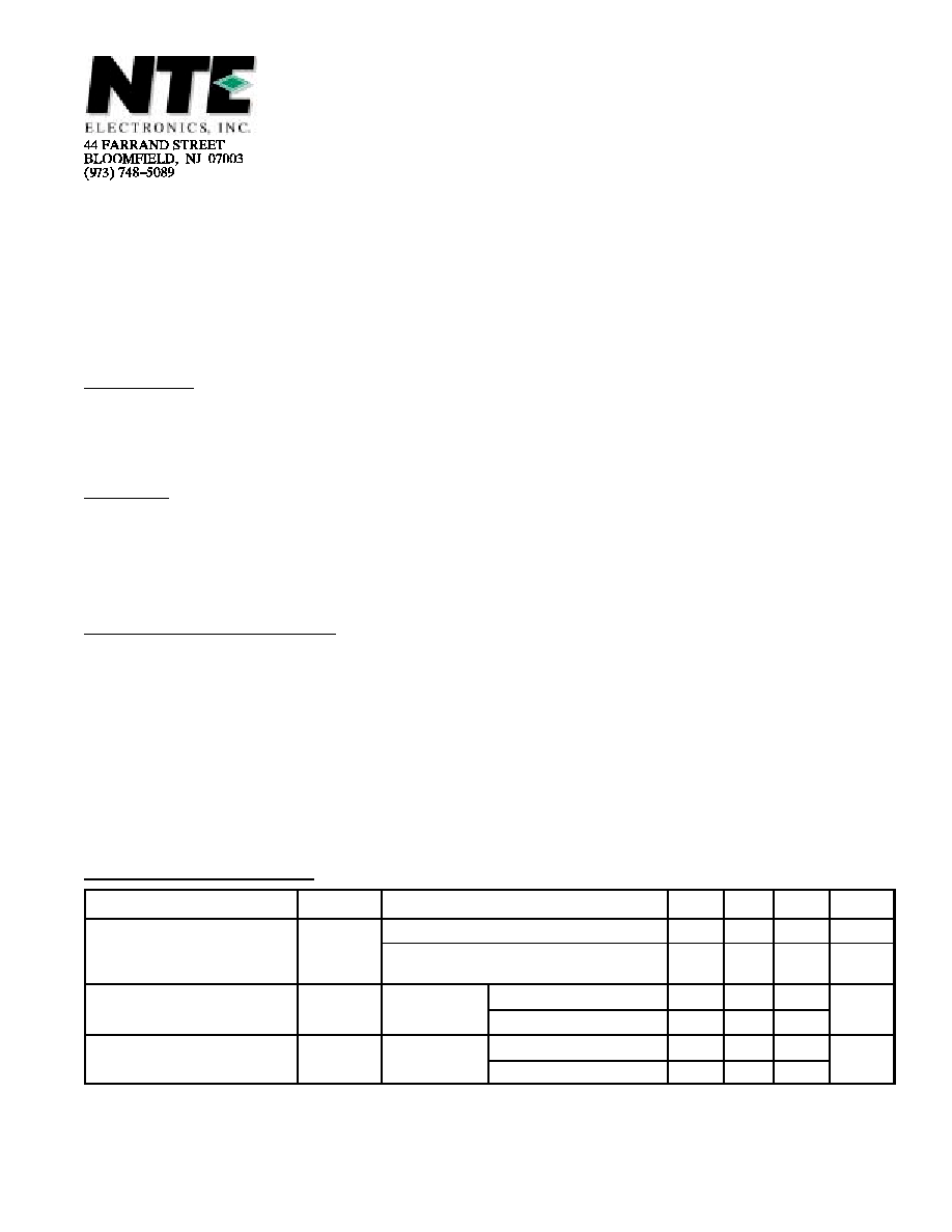
Electrical Characteristics: (V
IN
= ≠27V, I
O
= 500mA, T
J
= 0
∞
to +125
∞
C unless otherwise specified)
Parameter
Symbol
Test Conditions
Min
Typ
Max
Unit
Output Voltage
V
O
T
J
= +25
∞
C
≠17.3
≠18.0
≠18.7
V
5mA
I
O
1A, P
O
15W,
≠33V
V
IN
≠21V
≠17.1
≠18.0
≠18.9
V
Line Regulation
Reg
Line
T
J
= +25
∞
C,
≠33V
V
IN
≠21V
≠
25
360
mV
Note 1
≠30V
V
IN
≠24V
≠
10
180
Load Regulation
Reg
Load
T
J
= +25
∞
C,
5mA
I
O
1.5A
≠
55
360
mV
Note 1
250mA
I
O
750mA
≠
22
180
Electrical Characteristics: (V
IN
= ≠27V, I
O
= 500mA, T
J
= 0
∞
to +125
∞
C unless otherwise specified)
Parameter
Symbol
Test Conditions
Min
Typ
Max
Unit
Quiescent Current
I
B
T
J
= +25
∞
C
≠
4.5
8.0
mA
Quiescent Current Change
I
B
≠33V
V
IN
≠21V
≠
≠
1.0
mA
5mA
I
O
1A
≠
≠
0.5
Ripple Rejection
RR
32V
V
IN
21V, f = 120Hz
≠
57
≠
dB
Dropout Voltage
V
IN
≠ V
O
T
J
= +25
∞
C, I
O
= 1A
≠
2.0
≠
V
Output Noise Voltage
V
n
T
A
= +25
∞
C, 10Hz
f
100kHz
≠
10
≠
µ
V/V
O
Output Resistance
r
O
f = 1kHz
≠
19
≠
m
Short≠Circuit Current Limit
I
sc
T
A
= +25
∞
C, V
IN
= 35V
≠
0.2
≠
A
Peak Output Current
I
max
T
J
= +25
∞
C
≠
2.2
≠
A
Average Temperature
Coefficient of Output
Voltage
TCV
O
≠
≠1.1
≠
mV/
∞
C
Note 1. Load and line regulation are specified at constant junction temperature. Changes in V
O
due to heating effects must be taken into account spearately. Pulse testing with low duty
cycle is used.
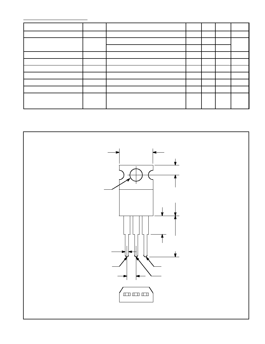
.420 (10.67)
Max
.500
(12.7)
Max
.500
(12.7)
Min
.250 (6.35)
Max
.147 (3.75)
Dia Max
.070 (1.78)
Max
.100 (2.54)
GND
V
IN
/Tab
V
OUT
.110 (2.79)