
Æ
CI0086
1
43 Gb/s 2: 1 SELECTOR
Features
Maximum output rate in multiplexing mode: 43 Gb/s
Output amplitude: 0.9 Vpp
Single-ended inputs
General Description
The CI0086 is a 2: 1 selector operating at rates up to 43 Gb/s output. The I/O levels are
SCFL (VH: 0.0 V, VL: -0.9 V). The IC is fabricated using a 0.1-µm InP HEMT process.
The CI0086 is provided in a hermetically-sealed package with V-connectors.
Applications
2: 1 Multiplexer
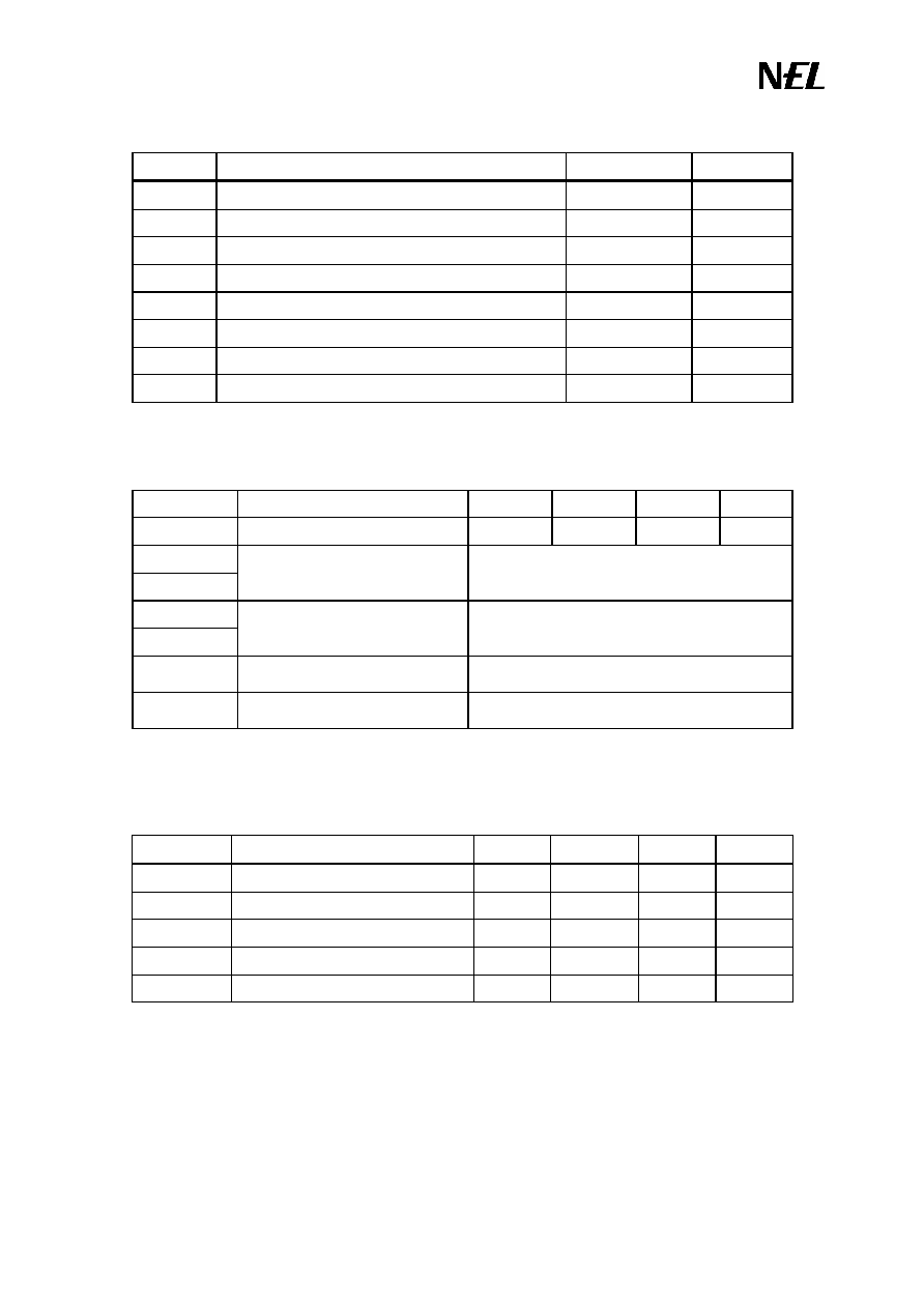
Functional Diagram
GD-01-1-60-42-123
28 Dec. 2001
SUGGESTED SPECIFICATION
D0
Q
QT
S
QC
D0
D1 S
D1
50
50
50
70
70

Æ
CI0086
3
Connection Table
No.
NAME FUNCTION No.
NAME FUNCTION
1 NC No Internal Connection
8
QT
(2)
Data Output (True)
2 S
Select Signal Input
9
QC
(2)
Data Output (Complementary)
3 GND
Ground (0.0 V)
10 GND
Ground (0.0 V)
4 Vrefd0
(1)
Data Input 0 Reference
11 Vss Power Supply (-4.5 V)
5 D0
Data Input 0
12 D1
Data Input 1
6 NC No Internal Connection
13 Vrefd1
(1)
Data Input 1 Reference
7 GND
Ground (0.0 V)
14 GND
Ground (0.0 V)
Notes
(1) Adjust Vrefd0 and Vrefd1 in the range between -0.75 V and -0.2 V.
(2) Terminate unused output to GND through 50 ohm resistors.
Connection Diagram (Top View)
NC
GND
GND
D0
QC
QT
S
NC
1
2
9
8
3
13
5
6
14
12
4
7
10
11
Vr
e
f
d
0
GND
Vss
GND
Vr
e
f
d
1
CI0086
D1
Æ
CI0086
4
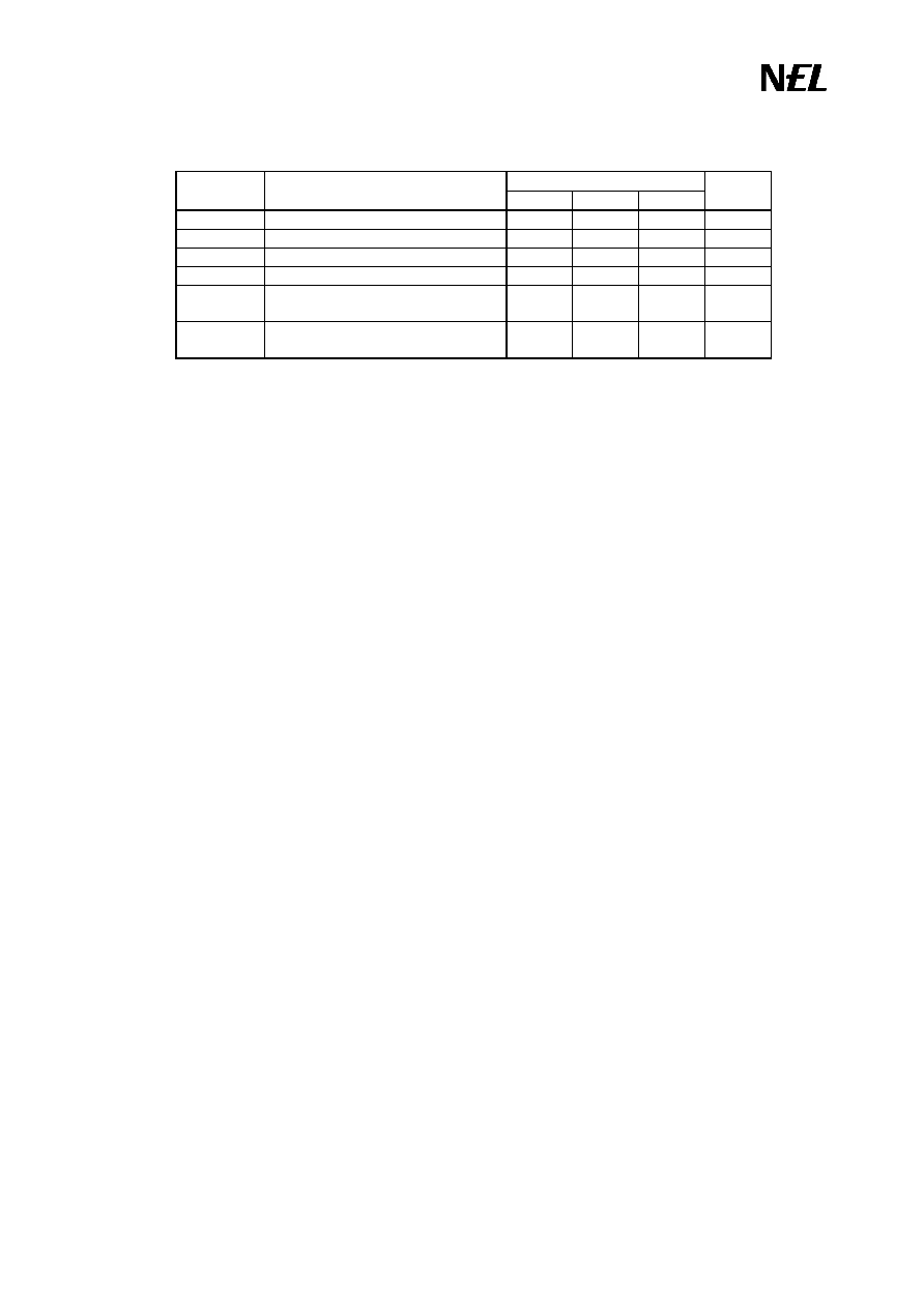
Absolute Maximum Ratings
SYMBOL PARAMETER
RATING
UNIT
VSS
Power Supply Voltage
-5.0 to +0.1
V
Vin
Applied Voltage Amplitude at Select Signal Input (S)
1.2 Vpp
Vind
Applied Voltage at Data Inputs (D0, D1)
-1.2 to +0.1
V
Vins
Applied Voltage at Select Signal Input (S)
-1.2 to +1.2
V
Vout
Applied Voltage at Data Outputs (QT, QC)
TBD V
Vrefd
Applied Voltage at Vrefd0 and Vrefd1 pin
-1.2 to +0.1
V
Tstor
Storage Temperature
TBD ∞C
Tc
(1)
Case Temperature under Bias
TBD ∞C
TBD: To Be Determined
Recommended Operating Conditions
SYMBOL PARAMETER MIN.
TYP.
MAX.
UNIT
VSS
Power Supply
-4.7 -4.5 -4.3 V
Vrefd0
Vrefd1
Data Input Reference Voltage
Adjust in the range from -0.75 V to -0.2 V
D0
D1
Data Input Interface
DC coupling (see DC Characteristics)
S
Select Signal Input Interface
DC coupling (see DC Characteristics) or
AC coupling (see AC Characteristics)
QT, QC
Data Output Interface
DC coupling (see DC Characteristics) ,
Terminate to GND through 50
DC Characteristics
(Vss = -4.5 V, GND = 0.0 V, Tc
(1)
= 30 ∞C)
SYMBOL PARAMETER MIN.
TYP.
MAX.
UNIT
ISS
Power Supply Current
420
TBD
mA
VOH
Output Voltage, High (QT, QC)
TBD 0.0 V
VOL
Output Voltage, Low (QT, QC)
-0.9
TBD
V
VIH
Input Voltage, High (D0, D1, S)
TBD 0.0 V
VIL
Input Voltage, Low (D0, D1, S)
-0.9
TBD
V
TBD: To Be Determined
Note
(1) Tc: Temperature at package base.
Æ
CI0086
5
AC Characteristics (43 GHz)
(Vss = -4.5 V, GND = 0.0 V, Vrefd0 and Vrefd1: Adjust in the range from -0.75 V to -0.2 V)
Tc=30
∞C
SYMBOL PARAMETER
MIN. TYP. MAX.
UNIT
Vin
Select Signal Input Voltage Amplitude
TBD 0.9 Vpp
f
MAX
Maximum Output Data Rate
43 Gb/s
S
MIN
Minimum Select Signal Frequency
10 GHz
Vamp
Output Voltage Amplitude (QT, QC)
TBD 0.9 Vpp
tr
Output Rise Time (QT, QC)
20 - 80%
10
TBD ps
tf
Output Fall Time (QT, QC)
20 - 80%
10
TBD ps
