 | –≠–ª–µ–∫—Ç—Ä–æ–Ω–Ω—ã–π –∫–æ–º–ø–æ–Ω–µ–Ω—Ç: IL422 | –°–∫–∞—á–∞—Ç—å:  PDF PDF  ZIP ZIP |

NVE Corporation
11409 Valley View Road
Eden Prairie, MN 55344-3617 USA
Telephone: (952) 829-9217
Fax: (952) 829-9189
Internet: www.isoloop.com
Functional Diagram
Features
∑
2500 V
RMS
Isolation (1 min)
∑
25 ns Propagation Delay
∑
25 MBaud Data Rate
∑
1 ns Pulse Skew (typ)
∑
±60 mA Driver Output Capability
∑
Thermal Shutdown Protection
∑
Meets or Exceeds EIA 422-B, EIA 485-A and
ITU Recommendation V11
∑
-40∞C to +85∞C Temperature Range
∑
16 Pin SOIC Package
∑
PROFIBUS International Component Recognition
∑
UL 1577 Approval (pending)
∑
IEC 61010-1 Approval (pending)
Applications
Multi-point or Multi-drop Transmission on Long Bus Lines
in Noisy Environments
Description
The IL422 is a galvanically isolated, high speed differential
driver and receiver pair, designed for bidirectional data
communication on balanced transmission lines. Isolation is
achieved through patented
*
Isoloop
Æ
technology. The IL422 is
the first isolated RS-422 interface available in a standard 16 pin
SOIC package, which meets the ANSI Standards EIA/TIA-422-B
and RS485.
The IL422 has current limiting and thermal shutdown features to
protect against output short circuits and bus contention situations
where these may cause excessive power dissipation.
Isolated RS422/RS485 Interface
Function Table
V
ID1
V
ID2
(Y-Z)
(A-B)
DE RE ISODE
R
D
MODE
X
0.2V
X
L
X
H
X
Receive
X
-
0.2V
X
L
X
L
X
Receive
-7<V
ID1
<12 -7<V
ID2
<12
X
H
X
Z
X
Receive/Drive
1.5
X
H
L
H
H
H
Drive
-1.5
X
H
L
H
L
L
Drive
Open
L
L
L
H
X
Receive
H= High Level, L= Low Level,
X= Irrelevant, Z= High Impedance
Isoloop
Æ
is a registered trademark of NVE Corporation
* US Patent number 5,831,426; 6,300,617 and others
Ordering Information
Order as IL422. If requesting tape and reel, please
specify as IL422TR.
IL422
I
SO
L
OOP
Æ
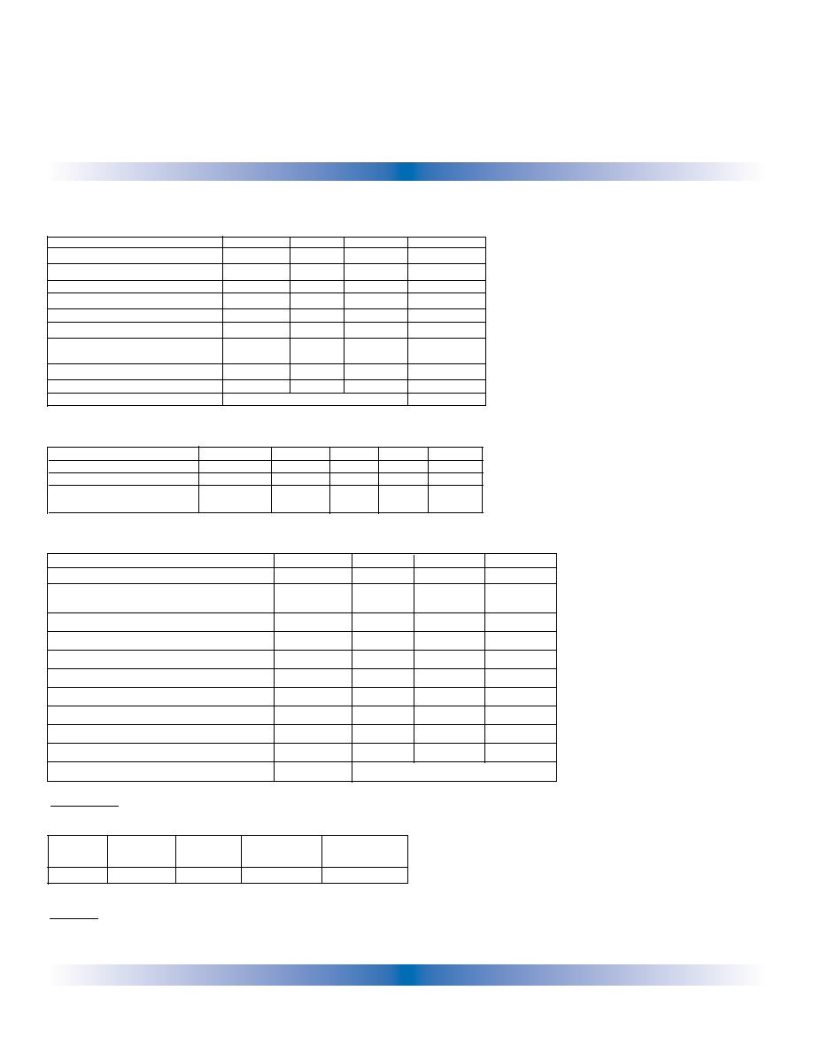
Recommended Operating Conditions
Parameters
Symbol
Min.
Max.
Units
Supply Voltage
V
DD
1,V
DD
2
4.5
5.5
V
Input Voltage at any bus terminal
V
I
12
V
(separately or common mode)
V
IC
-7
High-level Digital Input Voltage
V
IH
3.0
V
Low-Level Digital Input Voltage
V
IL
0.8
V
Differential Input Voltage
(2)
V
ID
±12
V
High-Level Output Current (Driver)
I
OH
-60
mA
High-Level Digital Output Current (Receiver)
I
OH
8
mA
Low-Level Output Current (Driver)
I
OL
60
mA
Low-Level Digital Output Current (Receiver)
I
OL
8
mA
Operating Free Air Temperature
T
A
-40
85
∞C
Digital Input Signal Rise and Fall Times
t
IR
,t
IF
DC Stable
Absolute Maximum Ratings
Parameters
Symbol
Min.
Max.
Units
Storage Temperature
T
S
-65
150
o
C
Ambient Operating Temperature
T
A
-40
85
o
C
Voltage Range at A or B Bus Pins
-7
12
V
Supply Voltage
(1)
V
DD
1,V
DD
2
-0.5
7
V
Digital Input Voltage
-0.5
5.5
V
Digital Output Voltage
-0.5
V
DD
+ 0.1
V
Continuous Total Power Dissipation
725
mW (25∞C)
377
mW (85∞C)
Maximum Output Current
I
O
95
mA
Lead Solder Temperature (10s)
260
∞C
ESD
2kV Human Body Model
Insulation Specifications
Parameter
Condition
Min.
Typ.
Max.
Units
Creepage Distance (External)
8.077
mm
Barrier Impedance
>10
14
||7
||
pF
Leakage Current
240 V
RMS
0.2
µ
A
60Hz
Model
Pollution
Material
Max Working
Package Type
Degree
Group
Voltage
IL422
II
III
400 V
RMS
16≠SOIC (0.3'')
IEC61010-1
TUV Certificate Numbers: Pending
Classification as Table 1.
UL 1577
Component Recognition program. File # Pending
Rated 2500Vrms for 1min.
2
NVE Corporation
11409 Valley View Road
Eden Prairie, MN 55344-3617 USA
Telephone: (612) 829-9217
Fax: (612) 829-9189
Internet: www.isoloop.com
IL422
I
SO
L
OOP
Æ

NVE Corporation
11409 Valley View Road
Eden Prairie, MN 55344-3617 USA
Telephone: (612) 829-9217
Fax: (612) 829-9189
Internet: www.isoloop.com
Driver Section
All Specifications are Tmin to Tmax unless otherwise stated.
Parameter
Symbol
Min.
Typ.
(5)
Max.
Units
Test Conditions
Input Clamp Voltage
V
IK
-1.5
V
I
L
=-18mA
Output Voltage
V
O
0
6
V
I
O
=0
Differential Output Voltage
|V
OD
1|
1.5
6
V
I
O
=0
Differential Output Voltage
(6)
|V
OD
2|
1.5
2.5
5
V
R
L
=54
Differential Output Voltage
V
OD
3
1.5
5
V
Vtest=-7 to 12V
Change in Magnitude of
(7)
|V
OD
|
±0.2
V
R
L
=54 or 100
Differential Output Voltage
Common Mode Output Voltage
V
OC
3
V
R
L
=54 or 100
-1
Change in Magnitude of
(7 )
|V
OC
|
±0.2
V
R
L
=54 or 100
Common Mode Output Voltage
Output Current
(4)
I
O
1
mA
Output Disabled V
O
=12
-0.8
mA
V
O
=-7
High Level Input Current
I
IH
10
µ
A
V1=3.5 V
Low Level Input Current
I
IL
-10
µ
A
V1=0.4 V
Short-Circuit Output Current
I
OS
-250
mA
V
O
= -6
-150
V
O
= 0
250
V
O
= 8
Supply Current (V
DD
2= +5V)
I
DD
2
27
34
mA
No Load (Outputs Enabled)
(V
DD
1= +5V)
I
DD
1
5
10
mA
Switching Characteristics
Parameter
Symbol
Min.
Typ.
(5)
Max.
Units
Test Conditions
Maximum Data Rate
25
Mbd
R
L
=54
, C
L
=50pF
Differential Output Delay Time
t
D
(
OD
)
16
25
ns
R
L
=54
, C
L
=50pF
Pulse Skew
(10)
t
SK
(
P
)
1
6
ns
R
L
=54
, C
L
=50pF
Differential Output Transition Time
t
T
(
OD
)
8
10
ns
R
L
=54
, C
L
=50pF
Output Enable Time To High Level
t
PZH
31
65
ns
R
L
=54
, C
L
=50pF
Output Enable Time To Low Level
t
PZL
22
35
ns
R
L
=54
, C
L
=50pF
Output Disable Time From High Level
t
PHZ
28
50
ns
R
L
=54
, C
L
=50pF
Output Disable Time From Low Level
t
PLZ
16
32
ns
R
L
=54
, C
L
=50pF
Skew Limit
(3)
t
SK
(
LIM
)
2
8
ns
R
L
=54
, C
L
=50pF
3
IL422
I
SO
L
OOP
Æ

Electrostatic Discharge Sensitivity
This product has been tested for electrostatic sensitivity to the limits stated in the specifications. However, NVE
recommends that all integrated circuits be handled with appropriate care to avoid damage. Damage caused by
inappropriate handling or storage could range from performance degradation to complete failure.
Receiver Section
All Specifications are Tmin to Tmax unless otherwise stated.
Parameter
Symbol
Min.
Typ.
(5)
Max.
Units
Test Conditions
Positive-going Input Threshold Voltage
V
IT
+
0.2
V
V
O
= 2.7V, Io= - 0.4mA
Negative-going Input Threshold Voltage
V
IT
-
-0.2
V
V
O
= 0.5V, Io= 8mA
Hysteresis Voltage (V
IT
+ - V
IT
-)
Vhys
60
mV
High Level Digital Output Voltage
V
OH
V
DD
- 0.1
V
V
ID
= 200mV, I
OH
= -20
µ
A
Low Level Digital Output Voltage
V
OL
0.2
V
V
ID
= -200mV, I
OL
= 20
µ
A
High-impedance-state output current
I
OZ
±10
µ
A
V
O
= 0.4 to (V
DD
2 - 0.5) V
Line Input Current
(8)
I
I
1
mA
Other Input
(11)
= 0V
V
I
=12V
-0.8
V
I
= ≠7V
Input Resistance
r
I
50
k
Supply Current (V
DD
2 = +5)
I
DD
2
27
34
mA
No Load (Outputs Enabled)
(V
DD
1 = +5)
I
DD
1
5
10
mA
Switching Characteristics
Parameter
Symbol
Min.
Typ.
(5)
Max.
Units
Test Conditions
Maximum Data Rate
25
Mbd
R
L
=54
, C
L
=50pF
Propagation Time
(9)
t
PD
24
32
ns
V
O
=-1.5 to 1.5V, C
L
=15pF
Pulse Skew
(10)
t
SK
(
P
)
1
6
ns
V
O
=-1.5 to 1.5V, C
L
=15pF
Skew Limit
(3)
t
SK
(lim)
2
8
ns
R
L
=54
, C
L
=50pF
Output Enable Time To High Level
t
PZH
17
24
ns
C
L
=15pF
Output Enable Time To Low Level
t
PZL
30
45
ns
C
L
=15pF
Output Disable Time From High Level
t
PHZ
30
45
ns
C
L
=15pF
Output Disable Time From Low Level
t
PLZ
18
27
ns
C
L
=15pF
4
IL422
I
SO
L
OOP
Æ
NVE Corporation
11409 Valley View Road
Eden Prairie, MN 55344-3617 USA
Telephone: (612) 829-9217
Fax: (612) 829-9189
Internet: www.isoloop.com
Notes:
1.
All Voltage values are with respect to network ground
except differential I/O bus voltages.
2.
Differential input/output voltage is measured at the
noninverting terminal A/Y with respect to the inverting
terminal B/Z.
3.
Skew limit is the maximum difference in any two channels
in one device.
4.
The power-off measurement in ANSI Standard
EIA/TIA-422-B applies to disabled outputs only and is not
applied to combined inputs and outputs.
5.
All typical values are at V
DD
1
,V
DD
2
= 5V and T
A
= 25∞C.
6.
The minimum V
OD
2
with a 100
load is either ΩV
OD
1
or
2V, whichever is greater.
7.
|
V
OD
| and
|V
OC
| are the changes in magnitude of V
OD
and V
OC
, respectively, that occur when the input is changed
form one logic state to the other.
8.
This applies for both power on and power off, refer to
ANSI standard RS-485 for exact condition. The EIA/TIA-
422-B limit does not apply for a combined driver and
receiver terminal.
9.
Includes 8 ns read enable time. Maximum propagation
delay is 25 ns after read assertion.
10. Pulse skew is defined as the |t
PLH
-t
PHL
| of each channel.
Application Notes:
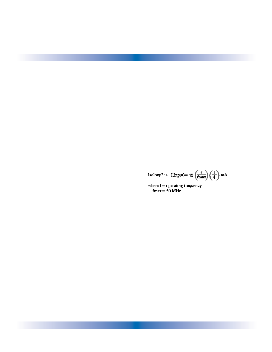
Power Consumption
Isoloop
devices achieve their low power consumption from
the manner by which they transmit data across the isolation
barrier. By detecting the edge transitions of the input logic
signal and converting these to narrow current pulses a
magnetic field is created around the GMR Wheatstone
bridge. Depending on the direction of the magnetic field,
the bridge causes the output comparator to switch following
the input logic signal. Since the current pulses are narrow,
about 2.5ns wide, the power consumption is independent of
mark-to-space ratio and solely dependent on frequency. This
has obvious advantages over optocouplers whose power
consumption is heavily dependent on its on-state and
frequency.
The approximate power supply current per channel for
Power Supplies
It is recommended that low ESR ceramic capacitors be
used to decouple the supplies. Both V
DD
1
and V
DD
2
should
be bypassed with 47 nF capacitors. These should be placed
no further than 1 cm from the device pins for proper
operation. In addition, V
DD
2
should have a 10
µ
F tantalum
capacitor connected in parallel with the 47 nF capacitor.
NVE Corporation
11409 Valley View Road
Eden Prairie, MN 55344-3617 USA
Telephone: (612) 829-9217
Fax: (612) 829-9189
Internet: www.isoloop.com
5
IL422
I
SO
L
OOP
Æ