 | –≠–ª–µ–∫—Ç—Ä–æ–Ω–Ω—ã–π –∫–æ–º–ø–æ–Ω–µ–Ω—Ç: IL716-3 | –°–∫–∞—á–∞—Ç—å:  PDF PDF  ZIP ZIP |
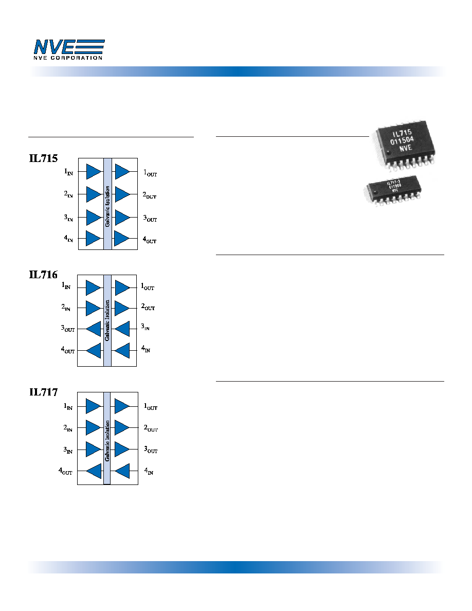
Functional Diagram
Features
∑
+5/3.3V or 5V CMOS/TTL Compatible
∑
High Speed: 110 MBaud
∑
2500 V
RMS
Isolation (1 min)
∑
2 ns Typical Pulse Width Distortion
∑
4 ns Typical Propagation Delay s Skew
∑
10 ns Typical Propagation Delay
∑
30 kV/
µs Typical Transient Immunity
∑
2 ns Channel to Channel Skew
∑
0.3'' and 0.15'' 16≠Pin SOIC Packages
∑
UL1577 Approved (File # E207481)
∑
IEC 61010-1 Approved (Report # 607057)
Isolation Applications
∑
ADCs and DACs
∑
Digital Fieldbus
∑
RS485 and RS422
∑
Multiplexed Data Transmission
∑
Data Interfaces
∑
Board-To-Board Communication
∑
Digital Noise Reduction
∑
Operator Interface
∑
Ground Loop Elimination
∑
Peripheral Interfaces
∑
Parallel Bus
∑
Logic Level Shifting
Description
NVE's family of high-speed digital isolators are CMOS devices created
by integrating active circuitry and our GMR-based and patented
*
IsoLoop
Æ
technology. The IL715, IL716 and IL717 are four channel
versions of the world's fastest digital isolator with a 110 Mbaud data
rate. These devices provide the designer with the most compact isolated
logic devices yet available. All transmit and receive channels operate at
110 Mbd over the full temperature and supply voltage range. The
symmetric magnetic coupling barrier provides a typical propagation
delay of only 10 ns and a pulse width distortion of 2 ns achieving the
best specifications of any isolator device. Typical transient immunity of
30 kV/µs is unsurpassed. The IL715 has four transmit channels; the
IL716 has two transmit channels and two receive channels; the IL717
has three transmit channels and one receive channel. The IL715, IL716
and IL717 high channel density make them ideally suited to isolating
ADCs and DACs, parallel buses and peripheral interfaces.
The IL715, IL716 and IL717 are available in 0.3" and 0.15" 16-pin
SOIC packages and performance is specified over the temperature range
of -40∞C to +100∞C without any derating.
High Speed Four Channel Digital Coupler
Isoloop
Æ
is a registered trademark of NVE Corporation
* US Patent number 5,831,426; 6,300,617 and others.
NVE Corporation 11409 Valley View Road Eden Prairie, MN 55344-3617 USA Telephone: (952) 829-9217 Fax: (952) 829-9189 Internet: www.isoloop.com
IL715/6/7
I
SO
L
OOP
Æ
Recommended Operating Conditions
Parameters
Symbol
Min.
Max.
Units
Ambient Operating Temperature
T
A
-40
100
o
C
Supply Voltage (3.3/5.0 V operation)
V
DD
1,V
DD
2
3.0
5.5
Volts
Supply Voltage (5.0 V operation)
V
DD
1,V
DD
2
4.5
5.5
Volts
Logic High Input Voltage
V
IH
2.4
V
DD
Volts
Logic Low Input Voltage
V
IL
0
0.8
Volts
Minimum Signal Rise and Fall Times
t
IR
,t
IF
1
µsec
Absolute Maximum Ratings
Parameters
Symbol
Min.
Max.
Units
Storage Temperature
T
S
-55
175
o
C
Ambient Operating Temperature
(1)
T
A
-55
125
o
C
Supply Voltage
V
DD
1,V
DD
2
-0.5
7
Volts
Input Voltage
V
I
-0.5
V
DD
+0.5
Volts
Output Voltage
V
O
-0.5
V
DD
+0.5
Volts
Output Current Drive Channel
I
O
10
mA
Lead Solder Temperature (10s)
280
o
C
ESD
2kV Human Body Model
Insulation Specifications
Parameter
Symbol
Min
Typ.
Max.
Units
Test Condition
Barrier Impedance
>10
14
||7
|| pF
Creepage Distance (External)
8.077 (0.3'' SOIC)
mm
4.026 (0.15'' SOIC)
Leakage Current
0.2
µA
240 V
RMS
Capacitance (Input-Output)
(5)
C
I
-
O
4.0
pF
f = 1MHz
Model
Pollution Material Max Working
Package Type
Degree
Group
Voltage
16≠SOIC (0.3'') 16≠SOIC (0.15'')
IL715, IL716, IL717
II
III
300 V
RMS
IL715-3, IL716-6, IL717-3
II
III
150 V
RMS
IEC61010-1
TUV Certificate Numbers: B 01 07 44230 003
Classification as Table 1.
UL 1577
Component Recognition program. File # E207481
Rated 2500Vrms for 1min.
* UL & IEC approval is pending for the 16-SOIC (0.15'') parts.
2
NVE Corporation 11409 Valley View Road Eden Prairie, MN 55344-3617 USA Telephone: (952) 829-9217 Fax: (952) 829-9189 Internet: www.isoloop.com
IL715/6/7
I
SO
L
OOP
Æ

Electrical Specifications
Electrical Specifications are Tmin to Tmax
Parameter
Symbol
3.3 Volt Specifications
5.0 Volt Specifications
Units
Test Conditions
DC Specifications
Min.
Typ.
Max.
Min.
Typ.
Max.
Input Quiescent Supply Current
IL715
I
DD
1
16
20
24
30
µA
IL716
I
DD
1
3.3
4
5
6
mA
IL717
I
DD
1
1.5
2.0
2.5
3.0
mA
Output Quiescent Supply Current
IL715
I
DD
2
5.5
8
8
12
mA
IL716
I
DD
2
3.3
4
5
6
mA
IL717
I
DD
2
3
6
6
9
mA
Logic Input Current
I
I
-10
10
-10
10
µA
Logic High Output Voltage
V
OH
V
DD
-0.1
V
DD
V
DD
-0.1
V
DD
V
I
O
=-20
µA, V
I
=V
IH
0.8*V
DD
V
DD
-0.5
0.8*V
DD
V
DD
-0.5
I
O
= -4 mA, V
I
=V
IH
Logic Low Output Voltage
V
OL
0
0.1
0
0.1
V
I
O
= 20
µA, V
I
=V
IL
0.5
0.8
0.5
0.8
I
O
= 4 mA, V
I
=V
IL
Switching Parameters
Maximum Data Rate
100
110
100
110
MBd
C
L
= 15 pF
Minimum Pulse Width
PW
10
10
ns
50% Points, V
O
Propagation Delay
Input to Output (High to Low)
t
PHL
12
18
10
15
ns
C
L
= 15 pF
Propagation Delay
Input to Output (Low to High)
t
PLH
12
18
10
15
ns
C
L
= 15 pF
Pulse Width Distortion
(2)
| tPHL- tPLH |
PWD
2
3
2
3
ns
C
L
= 15 pF
Propagation Delay Skew
(3)
t
PSK
4
6
4
6
ns
C
L
= 15 pF
Output Rise Time (10-90%)
t
R
2
4
1
3
ns
C
L
= 15 pF
Output Fall Time (10-90%)
t
F
2
4
1
3
ns
C
L
= 15 pF
Common Mode Transient
|CMH|
Immunity (Output Logic High
20
30
20
30
kV/
µs
Vcm = 300V
or Logic Low)
(4)
|CML|
Channel to Channel Skew
t
CSK
2
3
2
3
ns
C
L
= 15 pF
3
NVE Corporation 11409 Valley View Road Eden Prairie, MN 55344-3617 USA Telephone: (952) 829-9217 Fax: (952) 829-9189 Internet: www.isoloop.com
IL715/6/7
I
SO
L
OOP
Æ
Notes:
1.
Absolute Maximum ambient operating temperature means the
device will not be damaged if operated under these conditions. It
does not guarantee performance.
2.
PWD is defined as | t
PHL
≠ t
PLH
|. %PWD is equal to the PWD
divided by the pulse width.
3.
t
PSK
is equal to the magnitude of the worst case difference in t
PHL
and/or t
PLH
that will be seen between units at 25
O
C.
4.
CM
H
is the maximum common mode voltage slew rate that can be
sustained while maintaining V
O
> 0.8 V
DD
. CM
L
is the maximum
common mode input voltage that can be sustained while
maintaining V
O
< 0.8 V. The common mode voltage slew rates
apply to both rising and falling common mode voltage edges.
5.
Device is considered a two terminal device:
pins 1-8 shorted and pins 9-16 shorted.
4
Dynamic Power Consumption
Isoloop
devices achieve their low power consumption from the
manner by which they transmit data across the isolation barrier. By
detecting the edge transitions of the input logic signal and
converting these to narrow current pulses, a magnetic field is
created around the GMR Wheatstone bridge. Depending on the
direction of the magnetic field, the bridge causes the output
comparator to switch following the input logic signal. Since the
current pulses are narrow, about 2.5ns wide, the power
consumption is independent of mark-to-space ratio and solely
dependent on frequency. This has obvious advantages over
optocouplers whose power consumption is heavily dependent on
its on-state and frequency.
The approximate power supply current per channel for
Power Supply Decoupling
Both power supplies to these devices should be decoupled with
low ESR 47 nF ceramic capacitors. For data rates in excess of
10MBd, use of ground planes for both GND1 and GND2 is highly
recommended. Capacitors should be located as close as possible to
the device.
Signal Status on Start-up and Shut Down
To minimize power dissipation, the input signals are differentiated
and then latched on the output side of the isolation barrier to
reconstruct the signal. This could result in an ambiguous output
state depending on power up, shutdown and power loss
sequencing. Therefore, the designer should consider the inclusion
of an initialization signal in his start-up circuit. Initialization
consists of toggling each channel either high then low or low then
high, depending on the desired state.
Electrostatic Discharge Sensitivity
This product has been tested for electrostatic sensitivity to the
limits stated in the specifications. However, NVE recommends that
all integrated circuits be handled with appropriate care to avoid
damage. Damage caused by inappropriate handling or storage
could range from performance degradation to complete failure.
Data Transmission Rates
The reliability of a transmission system is directly related to the
accuracy and quality of the transmitted digital information. For a
digital system, those parameters which determine the limits of the
data transmission are pulse width distortion and propagation delay
skew.
Propagation delay is the time taken for the signal to travel through
the device. This is usually different when sending a low-to-high
than when sending a high-to-low signal. This difference, or error,
is called pulse width distortion (PWD) and is usually in ns. It may
also be expressed as a percentage:
This figure is almost three times better than for any available
optocoupler with the same temperature range, and two times better
than any optocoupler regardless of published temperature range.
The IsoLoop
Æ
range of isolators surpasses the 10% maximum
PWD recommended by PROFIBUS, and will run at almost 35 Mb
before reaching the 10% limit.
Propagation delay skew is the difference in time taken for two or
more channels to propagate their signals. This becomes significant
when clocking is involved since it is undesirable for the clock
pulse to arrive before the data has settled. A short propagation
delay skew is therefore critical, especially in high data rate parallel
systems, to establish and maintain accuracy and repeatability. The
IsoLoop
Æ
range of isolators all have a maximum propagation delay
skew of 6 ns, which is five times better than any optocoupler. The
maximum channel to channel skew in the IsoLoop
Æ
coupler is only
3 ns which is ten times better than any optocoupler.
Application Notes:
PWD% = Maximum Pulse Width Distortion (ns) x 100%
Signal Pulse Width (ns)
For example: For data rates of 12.5 Mb
PWD% =
3 ns
x 100% = 3.75%
80 ns
NVE Corporation 11409 Valley View Road Eden Prairie, MN 55344-3617 USA Telephone: (952) 829-9217 Fax: (952) 829-9189 Internet: www.isoloop.com
IL715/6/7
I
SO
L
OOP
Æ

5
NVE Corporation 11409 Valley View Road Eden Prairie, MN 55344-3617 USA Telephone: (952) 829-9217 Fax: (952) 829-9189 Internet: www.isoloop.com
IL715/6/7
I
SO
L
OOP
Æ
Applications:
Isolated Logic Level Shifters
CS
CLK
DI
DO
Sensor
ADC
IL717
Controller
+5V
+3.3V
GND 1
GND 2