PRELIMINARY PRODUCT SPECIFICATION
nDA10200x2-18a
Dual 10-bit 200 MSPS Digital-to-Analog Converter IP
Main office: Nordic VLSI ASA - Vestre Rosten 81, N-7075 Tiller, Norway - Phone +4772898900 - Fax +4772898989
Template ID:1159140_045 r.1.1A
Revision: 1.0B
Page 1 of 13
2003-04-10
FEATURES
∑ Dual 10-bit Current Output Transmit DAC
∑ Up to 200 MSPS Update Rate
∑ Single 1.8 V Power Supply
∑ Complementary Current Outputs
5 ≠ 15 mA Adjustable Full Scale Current
1.5 V p-p Differential Compliance Range
∑ Excellent Spurious-Free-Dynamic-Range
71 dBc at F
OUT
= 5 MHz
62 dBc at F
OUT
= 60 MHz
∑ Excellent Gain and Phase Matching
∑ Low Power Consumption
80 mW at 200 MSPS
∑ Power Saving Idle Modes
∑ Internal Voltage Reference
∑ 0.8 mm
2
Core Area
APPLICATIONS
∑ Communication Transmit Channel
WLAN / HiperLan / 802.11x
∑ Quadrature ( I and Q ) Modulation
∑ Digital Imaging / Video
∑ TV / Video / Radio Enecoders
∑ Graphic Encoders
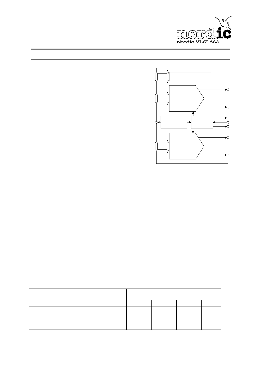
GENERAL DESCRIPTION
The nDA10200x2-18a is a monolithic, high speed,
low power, dual channel digital-to-analog
converter silicon IP. It uses a complementary
segmented current source architecture to provide
10-bit dynamic performance for update rates up to
200 MSPS. The core includes edge-triggered input
latches, an internal voltage reference and bias
circuitry that provides an adjustable full-scale
output current from 5 to 15 mA. The
complementary current outputs support a
compliance range of up to 1.5 V peak-to-peak
differential.
VOLTAGE
REFERENCE
CURRENT
BIAS
OPM[2:0]
CLK
DIGITAL CONTROL
VREF
VCAS0
IREF
D0[9:0]
CURRENT
OUTPUT
DAC
LA
TCH
IOUT0
IOUTC0
D1[9:0]
CURRENT
OUTPUT
DAC
LA
TC
H
IOUT1
IOUTC1
VCAS1
Figure 1. Functional block diagram
Designed specifically to address the transmit signal
path of broadband multicarrier communication
systems, it provides excellent dynamic
performance for output frequencies up to Nyquist
and beyond. The high performance also makes the
DAC ideal in applications like digital imaging and
video encoders. Combination of only 36 mW
power consumption and power saving idle modes,
makes the DAC very suitable for battery powered
operation.
Implemented in a generic 0.18
µm CMOS process,
operating from a single 1.8 V supply and
employing a fully differential architecture it
represents an ideal DAC for highly integrated
mixed signal systems.
.
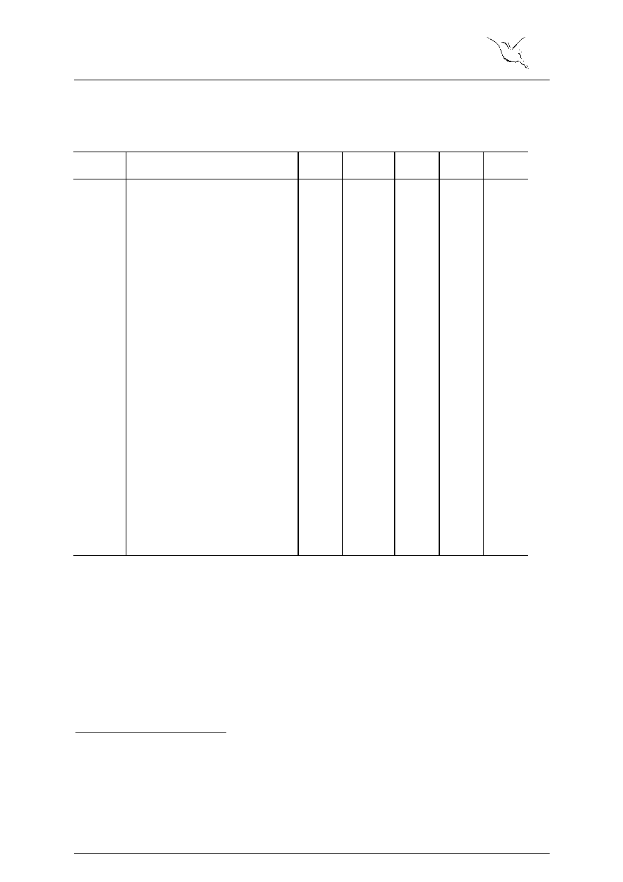
QUICK REFERENCE DATA
IP Type / Technology
Hard Macro / TSMC Generic, 6 Metal 0.18
µm CMOS
IP Area / Dimensions
0.8 mm
2
/ 0.8
◊ 1.0 mm
Parameter
Min.
Typ.
Max.
Unit
Supply Voltage
1.6
1.8
2.0
V
Power Dissipation, at 200 MSPS
80
mW
Differential Non Linearity
± 0.1
± 0.5
LSB
Integral Non Linearity
± 0.4
± 1.0
LSB
Spurious-Free-Dynamic Range, F
OUT
= 5 MHz
71
dBc
Table 1. nDA10200x2-18a quick reference data
PRELIMINARY PRODUCT SPECIFICATION
nDA10200x2-18a - Dual 10-bit 200 MSPS Digital-to-Analog Converter IP
Nordic VLSI
Page 2 of 13
Revision: 1.0B
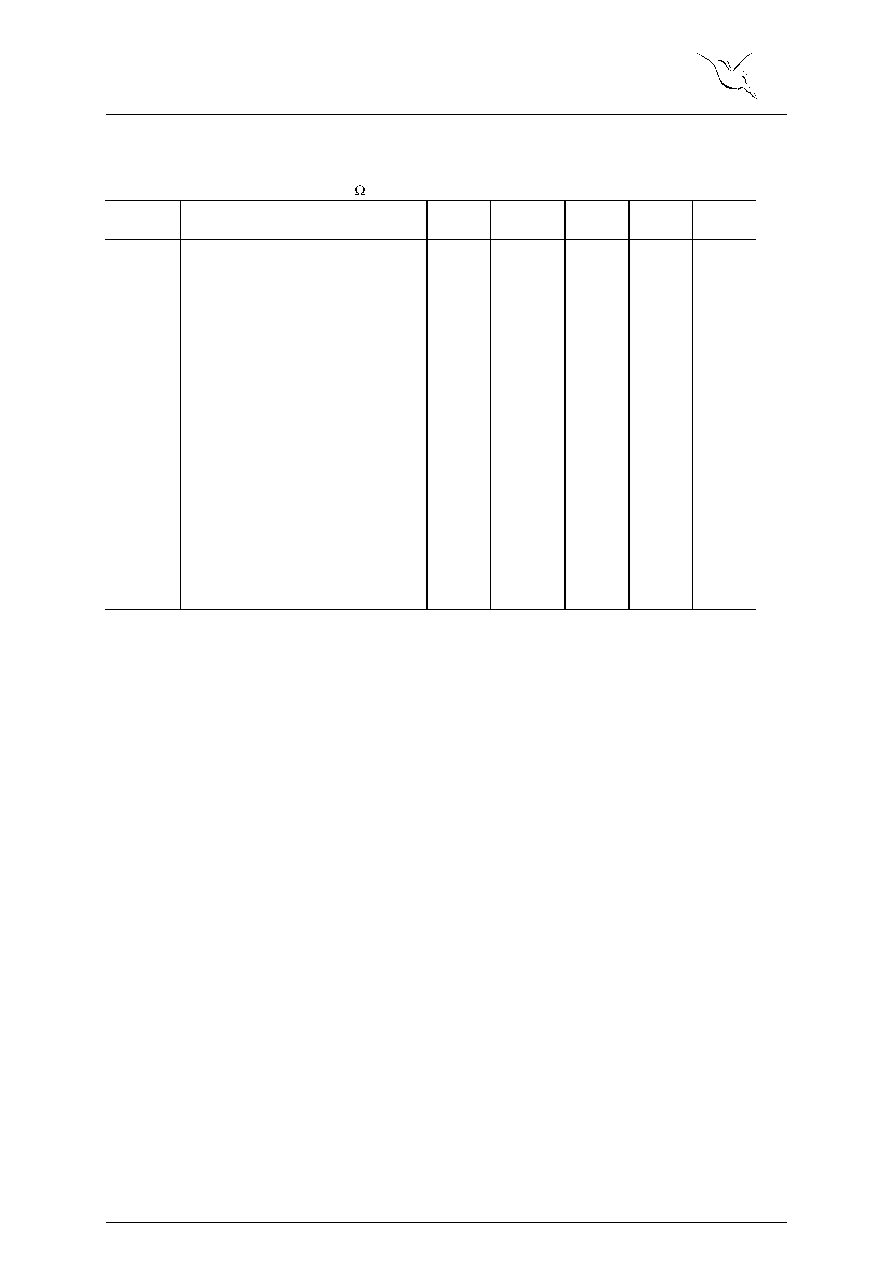
ELECTRICAL SPECIFICATIONS
DC SPECIFICATIONS
( At T
A
= 25 ∫C, V
AVDD
= V
VDD
= 1.8 V, F
CLK
= 200 MHz, I
FS
= 15 mA, unless otherwise noted )
Symbol
Parameter (condition)
Test
level
Min.
Typ.
Max.
Unit
DC ACCURACY
N
Resolution
10
Bits
INL
Integral Non Linearity
± 0.4
± 1.0
LSB
DNL
Differential Non Linearity
± 0.1
± 0.5
LSB
Monotonicity
Guarantied
ANALOG OUTPUT
Full-scale Output Current
5
15
mA
Output Compliance Range
0
0.75
Output Resistance
100
k
Output Capacitance
5
pF
Offset Error
-0.03
0.03
% of FSR
Gain Error ( With Internal Reference )
-10
± 3
+10
% of FSR
Gain Error ( With External Reference )
-3
± 0.5
+3
% of FSR
Gain Matching
-3
+3
% of FSR
REFERENCE VOLTAGE
Reference Voltage
1.18
1.22
1.26
V
Reference Voltage Drift
100
ppm /
∞C
POWER SUPPLY
Positive Supply Voltage
1.6
1.8
2.0
V
Negative Supply Voltage
GND
Supply Current, both Channels Active
40
mA
Supply Current, one Channel Active
22
mA
Supply Current, both Channels Sleep
1.8
mA
Supply Current, Power down
87
µA
Power Dissipation
1
, both Channels Active
72
mW
Power Dissipation
1
, both Channels Sleep
3.3
mW
Power Dissipation
1
, Power down
156
µW
Start-up time from Power down
2
65
µs
Start-up time from Sleep
2
0.5
µs
OPERATING CONDITIONS
Junction Operating Temperature
-40
125
∞C
Table 2. nDA10200x2-18a DC Specifications
1
Measured at V
AVDD
=1.8 V ,F
CLK
= 200 MSPS, I
FSR
=15 mA
2
10 nF VCAS0 and VCAS1 bypass, 100nF IREF and VREF bypass, V
AVDD
=1.8 V ,F
CLK
= 200 MSPS, I
FSR
=15 mA
PRELIMINARY PRODUCT SPECIFICATION
nDA10200x2-18a - Dual 10-bit 200 MSPS Digital-to-Analog Converter IP
Nordic VLSI
Page 3 of 13
Revision: 1.0B
DYNAMIC SPECIFICATIONS
(
T
A
= 25
∞C, V
DD
= 1.8V, I
FS
P$ GRXEO\ WHUPLQDWHG WUDQVIRUPHU FRXSOHG GLIIHUHQWLDO RXWSXW
)
Symbol
Parameter (condition)
Test
level
Min.
Typ.
Max.
Unit
DYNAMIC PERFORMANCE
Maximum Update Rate
200
MSPS
Glitch Impulse Energy
5
p-Vs
Output Rise Time
2.3
ns
Output Fall Time
2.3
ns
Output Noise ( I
FSR
= 15 mA )
50
pA / Hz
Ú
Output Noise ( I
FSR
= 5 mA )
30
pA / Hz
Ú
SPURIOUS FREE DYNAMIC RANGE
80 MSPS, F
OUT
= 5 MHz
73
dBc
80 MSPS, F
OUT
= 10 MHz
70
dBc
80 MSPS, F
OUT
= 20 MHz
64
dBc
80 MSPS, F
OUT
= 30 MHz
59
dBc
80 MSPS, F
OUT
= 39.5 MHz
60
dBc
200 MSPS, F
OUT
= 5 MHz
71
dBc
200 MSPS, F
OUT
= 20 MHz
69
dBc
200 MSPS, F
OUT
= 40 MHz
63
dBc
200 MSPS, F
OUT
= 60 MHz
62
dBc
200 MSPS, F
OUT
= 80 MHz
60
dBc
20 MSPS, F
OUT
= 94 MHz
59
dBc
CHANNEL ISOLATION
80 MSPS, F
OUT
= 39.5 MHz
60
dBc
200 MSPS, F
OUT
= 94 MHz
50
dBc
Table 3. nDA10200x2-18a Dynamic Specifications

PRELIMINARY PRODUCT SPECIFICATION
nDA10200x2-18a - Dual 10-bit 200 MSPS Digital-to-Analog Converter IP
Nordic VLSI
Page 4 of 13
Revision: 1.0B
DEFINITIONS OF SPECIFICATIONS
Integral Non Linearity ( INL )
The deviation of the DAC transfer function from
the ideal transfer function. The ideal transfer
function is defined as a straight line between the
end points of the transfer characteristic corrected
for gain and offset. INL for each code is calculated
at the code transitions.
Differential Non Linearity ( DNL )
In an ideal DAC every code transition to its
neighbours equals 1 LSB. DNL is the deviation of
each code transition from the ideal value.
Monotonicity
A DAC is monotonic if the output either increases
or remains constant if the digital input increases.
Output Compliance Range
The voltage range allowed at each current output.
Operation beyond this range will result in nonlinear
performance or breakdown
Gain Error
The deviation of the actual difference between the
first and last code transition and the ideal
difference.
Offset Error
Mid output ideally occurs for mid code input. The
offset error is the difference of the actual output at
mid code input and the ideal mid output.
Temperature Drift
The temperature drift specifies the maximum
change from the nominal junction temperature to
the minimum and maximum junction temperature.
Maximum Update Rate
The maximum update rate is the highest update rate
at which electrical specifications are tested.
Minimum Update Rate
The minimum update rate is the lowest update rate
where the DAC is functional.
Clock Duty Cycle
The fraction of the time the clock spends above the
logic threshold.
Glitch Impulse Energy
The net area of undesired output transients at a
code transition measured in pV-s.
Latency
The latency is the time it takes from a digital input
is latched in, to the sample is converted and put on
the analog output.
Propagation Delay ( t
PD
)
Propagation delay is the time from the clock edge
that defines output data transition to the output data
starts to change.
Output Rise Time
The time required the output to rise from 10 % to
90 % of a full-scale transition.
Output Fall Time
The time required the output to fall from 90 % to
10 % of a full-scale transition.
Settling Time
The time it takes for the output to reach and remain
within a specified absolute error measured from the
start of the transition.
Output Noise
Output noise density with a dc signal input.
Spurious-Free Dynamic Range ( SFDR )
SFDR is the amplitude difference between the
measured output signal and the highest harmonic
component.

PRELIMINARY PRODUCT SPECIFICATION
nDA10200x2-18a - Dual 10-bit 200 MSPS Digital-to-Analog Converter IP
Nordic VLSI
Page 5 of 13
Revision: 1.0B
ABSOLUTE MAXIMUM RATINGS
1
Pin / Condition
Min
Max
Unit
All pins referred to AVSS pin
-0.2
2.2
V
Operating Junction Temperature
-40
125
∞C
Storage Temperature
-65
125
∞C
Table 4. Absolute maximum ratings
EXPLANATION OF TEST LEVELS
Test Level I:
100% production tested at +25∞C
Test Level II:
100% production tested at +25∞C and sample tested at specified temperatures
Test Level III:
Sample tested only
Test Level IV:
Parameter is guaranteed by design and characterization testing
Test Level V:
Parameter is typical value only
Test Level VI:
100% production tested at +25∞C. Guaranteed by design and characterization testing for
industrial temperature range
COMPLETE PINOUT LIST
Name
Type
1)
Description
D0[9:0]
DI
Input Data Bits for Channel 0. D0[9] is MSB, D0[0] is LSB
D1[9:0]
DI
Input Data Bits for Channel 1. D1[9] is MSB, D1[0] is LSB
CLKA
DI
Conversion Clock A
CLKB
DI
Conversion Clock B
CLKBSEL
DI
Conversion Clock B Select.
CLK_OUT
DO
Reference Clock Output
OPM[2:0]
DI
Operational Mode Control both Channels
IOUT0, IOUTC0
AO
Complementary Current Outputs for Channel 0
IOUT1, IOUTC1
AO
Complementary Current Outputs for Channel 1
VCAS0
AB
Decoupling pin for Channel 0. Bypass with at least 10nF to AVDDCS0
VCAS1
AB
Decoupling pin for Channel 0. Bypass with at least 10nF to AVDDCS1
IREF
AI
Full-scale Current Reference both Channels
VREF
AB
Voltage Reference
AVDDCS0
AP
Positive 1.8 V Supply, Channel 0 Current Sources
AVDDCS1
AP
Positive 1.8 V Supply, Channel 1 Current Sources
AVDD
AP
Positive 1.8 V Supply both Channels
AVSS
AG
Ground
1) D = Digital, A = Analog, I = In, O = Out, B = Bidirectional, T = Tristate, P = Power, G = Ground.
Table 5. nDA10200x2-18a pinout list
1
Stress above one or more of the limiting values may cause permanent damage to the device