1/26
° Semiconductor
MSM82C51A-2RS/GS/JS
GENERAL DESCRIPTION
The MSM82C51A-2 is a USART (Universal Synchronous Asynchronous Receiver Transmitter)
for serial data communication.
As a peripheral device of a microcomputer system, the MSM82C51A-2 receives parallel data
from the CPU and transmits serial data after conversion. This device also receives serial data
from the outside and transmits parallel data to the CPU after conversion.
The MSM82C51A-2 configures a fully static circuit using silicon gate CMOS technology.
Therefore, it operates on extremely low power at 100 mA (max) of standby current by
suspending all operations.
FEATURES
∑ Wide power supply voltage range from 3 V to 6 V
∑ Wide temperature range from ≠40
∞
C to 85
∞
C
∑ Synchronous communication upto 64 Kbaud
∑ Asynchronous communication upto 38.4 Kbaud
∑ Transmitting/receiving operations under double buffered configuration.
∑ Error detection (parity, overrun and framing)
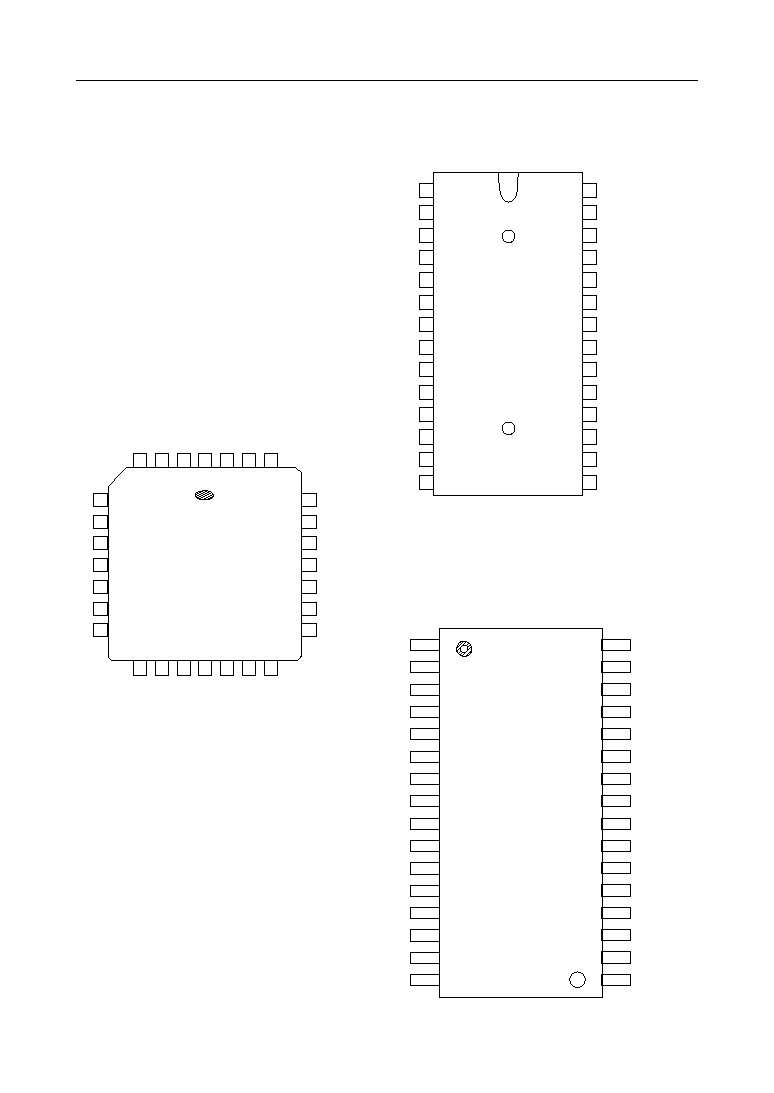
∑ 28-pin Plastic DIP (DIP28-P-600-2.54): (Product name: MSM82C51A-2RS)
∑ 28-pin Plastic QFJ (QFJ28-P-S450-1.27): (Product name: MSM82C51A-2JS)
∑ 32-pin Plastic SSOP(SSOP32-P-430-1.00-K): (Product name: MSM82C51A-2GS-K)
° Semiconductor
MSM82C51A-2RS/GS/JS
UNIVERSAL SYNCHRONOUS ASYNCHRONOUS RECEIVER TRANSMITTER
E2O0017-27-X2
This version: Jan. 1998
Previous version: Aug. 1996
4/26
° Semiconductor
MSM82C51A-2RS/GS/JS
FUNCTION
Outline
The MSM82C51A-2's functional configuration is programed by software.
Operation between the MSM82C51A-2 and a CPU is executed by program control. Table 1
shows the operation between a CPU and the device.
0
0
0
Data Bus 3-State
1
Data Bus 3-State
CS
•
1
1
•
C/
D
Status ∆ CPU
Control Word ® CPU
1
1
0
•
0
Data ® CPU
0
Data ∆ CPU
0
0
0
1
WR
1
0
1
•
1
0
RD
Table 1 Operation between MSM82C51A and CPU
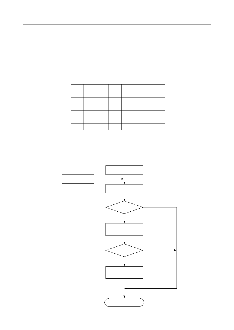
It is necessary to execute a function-setting sequence after resetting the MSM82C51A-2. Fig. 1
shows the function-setting sequence.
If the function was set, the device is ready to receive a command, thus enabling the transfer of
data by setting a necessary command, reading a status and reading/writing data.
Asynchronous
External Reset
Internal Reset
Write Mode Instruction
Write First Sync
Charactor
yes
no
Single
Sync Mode
Write Second Sync
Charactor
yes
no
End of Mode Setting
Fig. 1 Function-setting Sequence (Mode Instruction Sequence)

5/26
° Semiconductor
MSM82C51A-2RS/GS/JS
Control Words
There are two types of control word.
1. Mode instruction (setting of function)
2. Command (setting of operation)
1) Mode Instruction
Mode instruction is used for setting the function of the MSM82C51A-2. Mode instruction
will be in "wait for write" at either internal reset or external reset. That is, the writing of a
control word after resetting will be recognized as a "mode instruction."
Items set by mode instruction are as follows:
∑
Synchronous/asynchronous mode
∑
Stop bit length (asynchronous mode)
∑
Character length
∑
Parity bit
∑
Baud rate factor (asynchronous mode)
∑
Internal/external synchronization (synchronous mode)
∑
Number of synchronous characters (Synchronous mode)
The bit configuration of mode instruction is shown in Figures 2 and 3. In the case of
synchronous mode, it is necessary to write one-or two byte sync characters.
If sync characters were written, a function will be set because the writing of sync characters
constitutes part of mode instruction.
S
1
S
1
EP
PEN
L
2
L
1
B
2
B
1
D
7
D
6
D
5
D
4
D
3
D
2
D
1
D
0
0
1
0
1
0
0
1
1
Refer to
Fig. 3
SYNC
1 •
16 •
64 •
Baud Rate Factor
0
1
0
0
0
1
5 bits
6 bits
7 bits
Charactor Length
1
1
8 bits
0
1
0
1
0
0
1
1
Disable
Odd
Parity
Disable
Even
Parity
Parity Check
0
1
0
0
0
1
Inhabit
1 bit
1.5 bits
Stop bit Length
1
1
2 bits
Fig. 2 Bit Configuration of Mode Instruction (Asynchronous)