1/26
° Semiconductor
MSM82C55A-2RS/GS/VJS
GENERAL DESCRIPTION
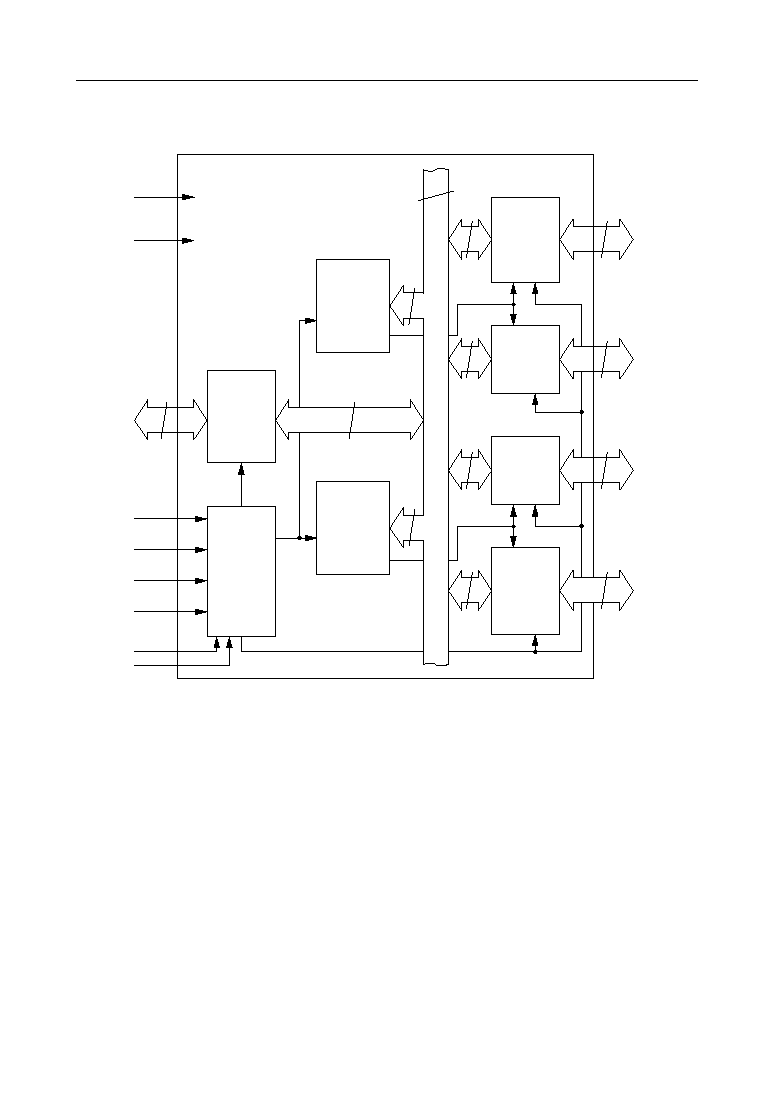
The MSM82C55A-2 is a programmable universal I/O interface device which operates as high
speed and on low power consumption due to 3m silicon gate CMOS technology. It is the best
fit as an I/O port in a system which employs the 8-bit parallel processing MSM80C85AH CPU.
This device has 24-bit I/O pins equivalent to three 8-bit I/O ports and all inputs/outputs are
TTL interface compatible.
FEATURES
∑ High speed and low power consumption due to 3m silicon gate CMOS technology
∑ 3 V to 6 V single power supply
∑ Full static operation
∑ Programmable 24-bit I/O ports
∑ Bidirectional bus operation (Port A)
∑ Bit set/reset function (Port C)
∑ TTL compatible
∑ Compatible with 8255A-5
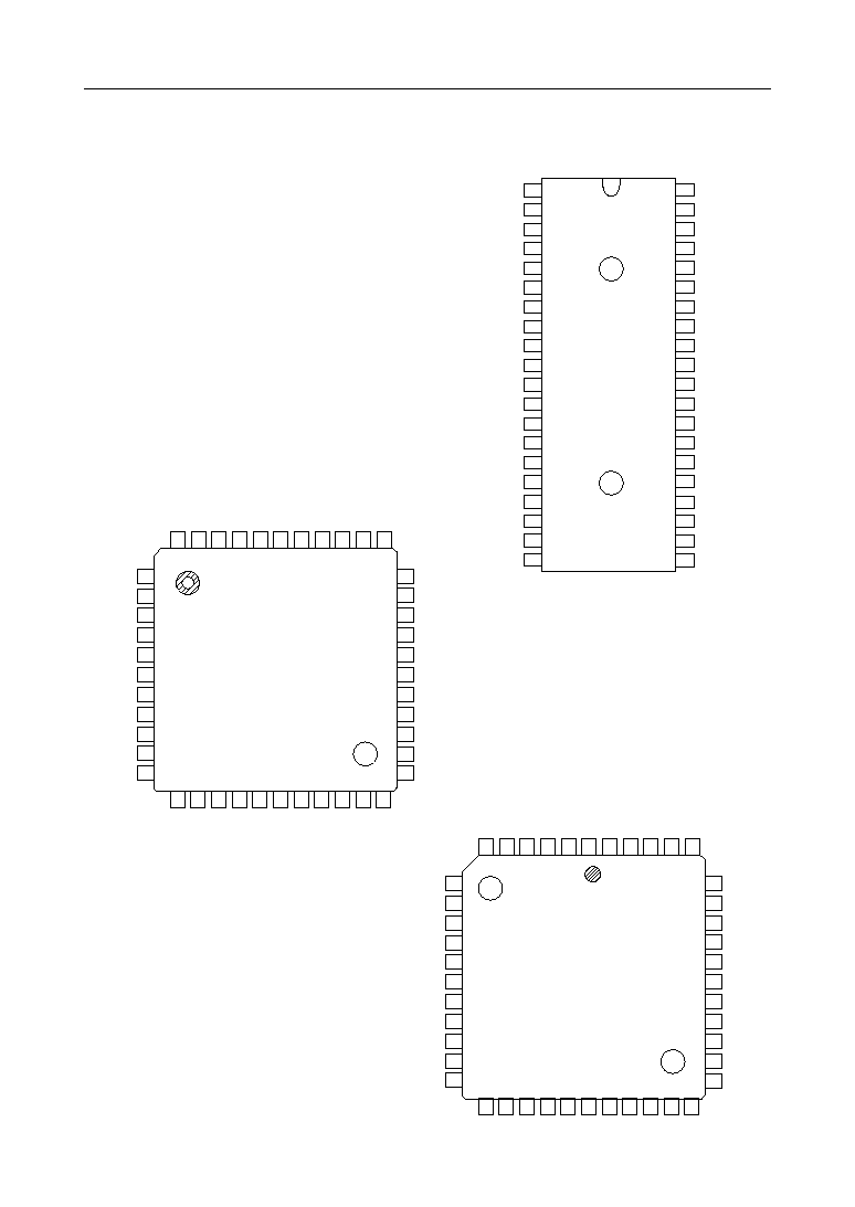
∑ 40-pin Plastic DIP (DIP40-P-600-2.54): (Product name: MSM82C55A-2RS)
∑ 44-pin Plastic QFJ (QFJ44-P-S650-1.27): (Product name: MSM82C55A-2VJS)
∑ 44-pin Plastic QFP (QFP44-P-910-0.80-2K): (Product name: MSM82C55A-2GS-2K)
° Semiconductor
MSM82C55A-2RS/GS/VJS
CMOS PROGRAMMABLE PERIPHERAL INTERFACE
E2O0020-27-X3
This version: Jan. 1998
Previous version: Aug. 1996
4/26
° Semiconductor
MSM82C55A-2RS/GS/VJS
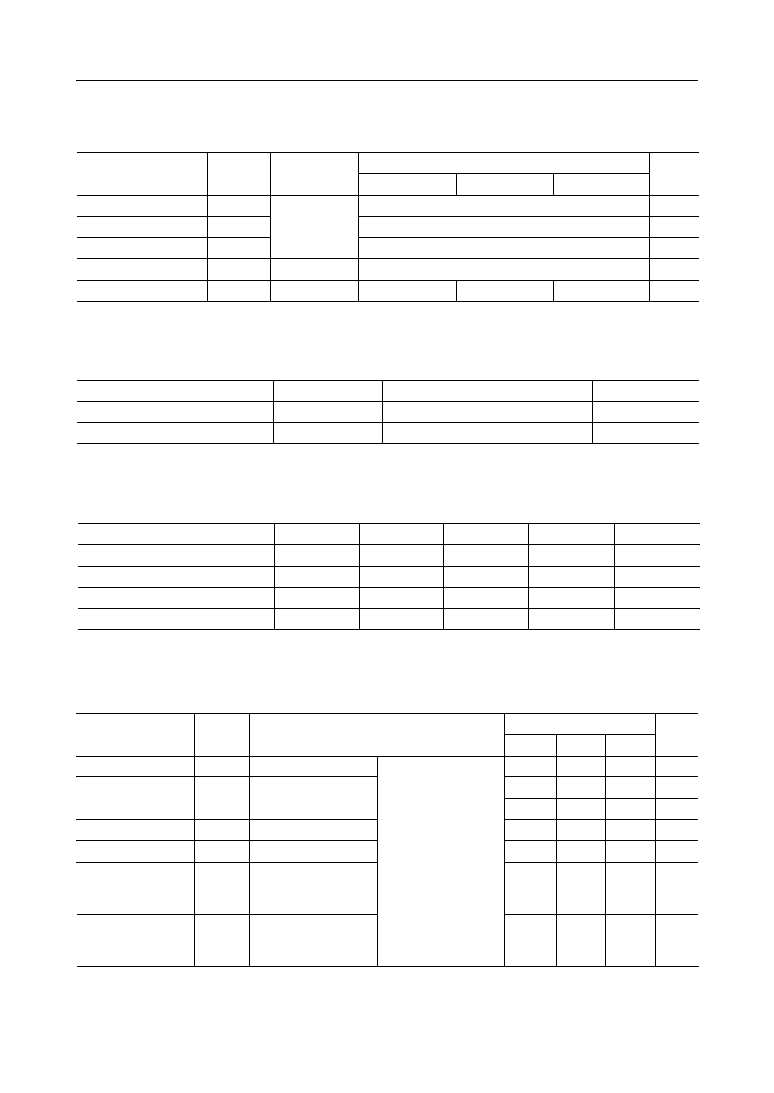
ABSOLUTE MAXIMUM RATINGS
≠55 to +150
MSM82C55A-2RS
Supply Voltage
V
CC
≠0.5 to +7
V
Input Voltage
V
IN
≠0.5 to V
CC
+0.5
V
Output Voltage
V
OUT
≠0.5 to V
CC
+0.5
V
Storage Temperature
T
STG
∞C
Power Dissipation
P
D
0.7
W
Parameter
Unit
Symbol
--
Ta = 25∞C
Conditions
Rating
MSM82C55A-2GS MSM82C55A-2vJS
1.0
1.0
Ta = 25∞C
with respect
to GND
OPERATING RANGE
Supply Voltage
V
CC
V
T
op
Range
3 to 6
≠40 to 85
Parameter
Unit
Symbol
∞C
Operating Temperature
RECOMMENDED OPERATING RANGE
DC CHARACTERISTICS
Typ.
Supply Voltage
V
CC
5
V
T
op
+25
"L" Input Voltage
V
IL
--
"H" Input Voltage
V
IH
--
Min.
4.5
≠40
≠0.3
2.2
Max.
5.5
+85
+0.8
V
CC
+ 0.3
Parameter
Unit
Symbol
∞C
V
V
Operating Temperature
Typ.
Max.
"L" Output Voltage
V
OL
0.4
V
"H" Output Voltage
V
OH
--
V
--
V
Parameter
Unit
Symbol
Min.
--
4.2
3.7
I
OL
= 2.5 mA
I
OH
= ≠40
mA
I
OH
= ≠2.5 mA
Conditions
V
CC
= 4.5 V to 5.5 V
Ta
= ≠40∞C to +85∞C
(C
L
= 0 pF)
Input Leak Current
I
LI
1
mA
Output Leak Current
I
LO
10
mA
≠1
≠10
0
£ V
IN
£ V
CC
0
£ V
OUT
£ V
CC
CS V
CC
≠0.2 V
V
IH
V
CC
≠0.2 V
V
IL
£
0.2 V
Supply Current
(Standby)
I
CCS
mA
8
mA
--
--
I/O Wire Cycle
82C55A-2
...8 MHzCPU Timing
I
CC
Average Supply
Current (Active)
10
--
--
--
--
--
0.1
--
MSM82C55A-2

5/26
° Semiconductor
MSM82C55A-2RS/GS/VJS
AC CHARACTERISTICS
Min.
Max.
Setup Time of Address to the Falling Edge of RD
t
AR
20
--
ns
Hold Time of Address to the Rising Edge of RD
t
RA
0
--
ns
Parameter
Unit
Symbol
Remarks
Setup Time of Address before the Falling Edge of WR
t
AW
0
--
ns
Load
150 pF
(V
CC
= 4.5 V to 5.5 V, Ta = ≠40 to +85∞C)
MSM82C55A-2
Delay Time from the Falling Edge of RD to the Output of
Defined Data
t
RD
--
120
ns
Delay Time from the Rising Edge of RD to the Floating of
Data Bus
t
DF
10
75
ns
Time from the Rising Edge of RD or WR to the Next Falling
Edge of RD or WR
t
RV
200
--
ns
RD Pulse Width
t
RR
100
--
ns
Hold Time of Address after the Rising Edge of WR
t
WA
20
--
ns
WR Pulse Width
t
WW
150
--
ns
Setup Time of Bus Data before the Rising Edge of WR
t
DW
50
--
ns
Hold Time of Bus Data after the Rising Edge of WR
t
WD
30
--
ns
Delay Time from the rising Edge of WR to the Output of
Defined Data
t
WB
--
200
ns
Setup Time of Port Data before the Falling Edge of RD
t
IR
20
--
ns
Hold Time of Port Data after the Rising Edge of RD
t
HR
10
--
ns
ACK Pulse Width
t
AK
100
--
ns
STB Pulse Width
t
ST
100
--
ns
Setup Time of Port Data before the rising Edge of STB
t
PS
20
--
ns
Hold Time of Port Bus Data after the rising Edge of STB
t
PH
50
--
ns
Delay Time from the Falling Edge of ACK to the Output of
Defined Data
t
AD
--
150
ns
Delay Time from the Rising Edge of ACK to the Floating of
Port (Port A in Mode 2)
t
KD
20
250
ns
Delay Time from the Rising Edge of WR to the Falling Edge of
OBF
t
WOB
--
150
ns
Delay Time from the Falling Edge of ACK to the Rising Edge of
OBF
t
AOB
--
150
ns
Delay Time from the Falling Edge of STB to the Rising Edge of
IBF
t
SIB
--
150
ns
Delay Time from the Rising Edge of RD to the Falling Edge of
IBF
t
RIB
--
150
ns
Delay Time from the the Falling Edge of RD to the Falling Edge
of INTR
t
RIT
--
200
ns
Delay Time from the Rising Edge of STB to the Rising Edge of
INTR
t
SIT
--
150
ns
Delay Time from the Rising Edge of ACK to the Rising Edge of
INTR
t
AIT
--
150
ns
Delay Time from the Falling Edge of WR to the Falling Edge of
INTR
t
WIT
--
250
ns
Note: Timing measured at V
L
= 0.8 V and V
H
= 2.2 V for both inputs and outputs.