1/14
KGF1256B/1256
° electronic components
This version: Jul. 1998
Previous version: Jan. 1998
GENERAL DESCRIPTION
The KGF1256B is a medium-power amplifier, with frequencies ranging from the UHF-band to
the L-band, that features high output power, low noise, and low current operation. The
KGF1256B specifications are guaranteed to a fixed matching circuit for 5 V and 850 MHz; external
impedance-matching circuits are also required. Because of the low noise and high output power
at the low operating current, the KGF1256B is ideal as a transmitter-driver amplifier for personal
handy phones.
The KGF1256 is similar to the KGF1256B in specifications and typical properties. Although
having S Parameters that are slightly different from those of the KGF1256B, the KGF1256 meets
the specifications for the KGF1256B, even with the same matching circuits.
FEATURES
∑ High output power: 15 dBm (min.)
∑ Low noise: 2.5 dB (max.)
∑ Low current: 40 mA (max.)
∑ Self-bias circuit configuration with built-in source capacitor
∑ Package: 4PSOP
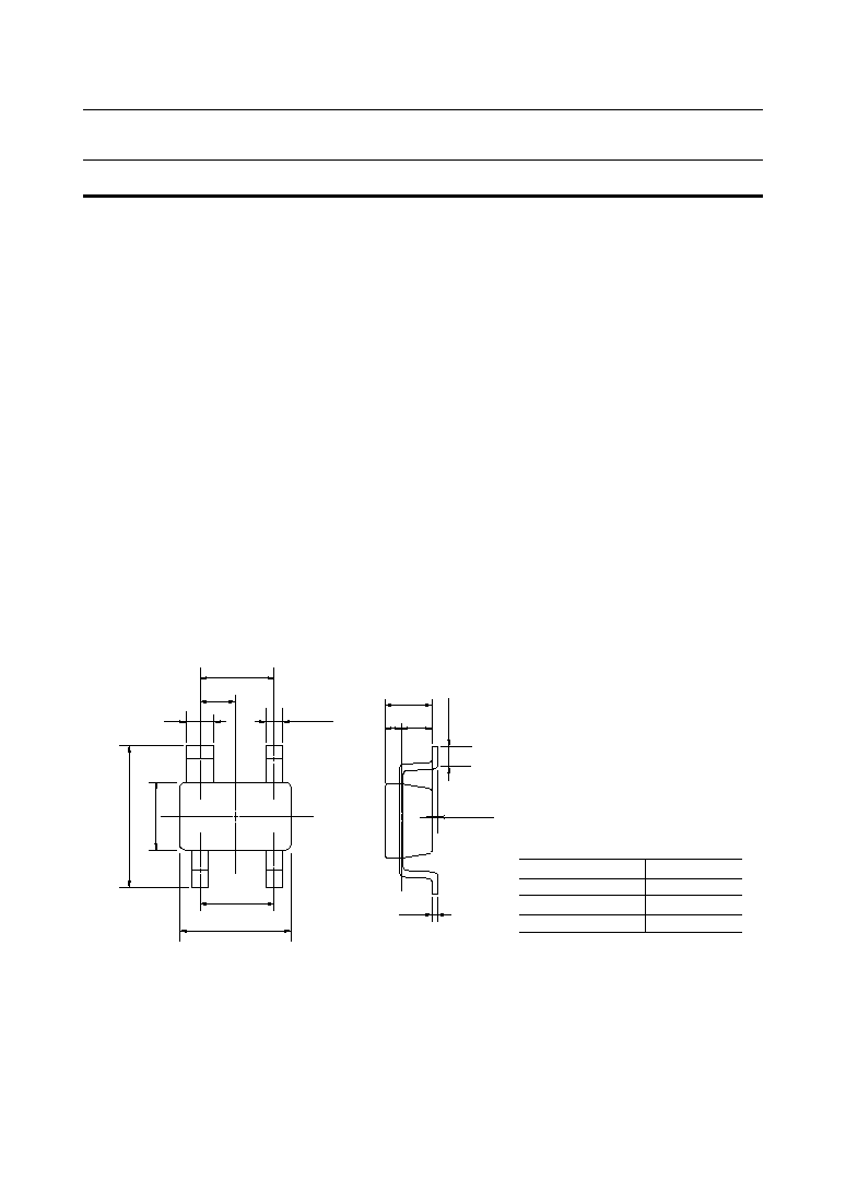
PACKAGE DIMENSIONS
°
electronic components
KGF1256B/1256
Medium-Power Amplifier
E2Q0024-38-71
Note: Ask our sales department for detailed requirements of the KGF1256.
1.5±0.15
3.0±0.2
0.3 MIN
0.6
+0.1
≠0.05
0.4
+0.1
≠0.05
1.8±0.1
0.85±0.05
1.9±0.1
2.8±0.15
0 to 0.15
0.125
+0.03
≠0
1.1±0.15
0.36 0.74
(Unit: mm)
Package material
Pin treatment
Solder plate thickness
Lead frame material
Epoxy resin
Solder plating
5 mm or more
42 alloy

2/14
KGF1256B/1256
° electronic components
MARKING
CIRCUIT
X
ALPHABETICAL
NUMERICAL
PRODUCT TYPE
LOT
NUMBER
(1)
X
D
(2)
(4)
(3)
(1) Gate
(2) Source
(3) Drain
(4) GND
Gate(1)
GND(4)
Drain(3)
Source(2)

3/14
KGF1256B/1256
° electronic components
ABSOLUTE MAXIMUM RATINGS
ELECTRICAL CHARACTERISTICS
*1 Self-bias condition: V
DD
= 5
±
0.25 V, V
G
= 0 V
*2 Self-bias condition: V
DD
= 3 V, V
G
= 0 V
Item
V
DS
Symbol
Condition
Max.
Unit
Drain-source voltage
Gate-source voltage
Total power dissipation
Channel temperature
V
GS
P
tot
T
ch
Ta = 25∞C
--
7
0.4
300
150
V
V
mW
∞C
Storage temperature
T
stg
--
125
∞C
Min.
--
≠3.0
--
--
≠45
Ta = 25∞C
Ta = 25∞C
Drain current
I
DS
Ta = 25∞C
360
mA
--
Item
I
GSS
Symbol
Condition
Max.
Unit
Gate-source leakage current
72
--
--
--
mA
dB
--
Min.
--
14.0
--
--
--
(*1), P
IN
=
≠20 dBm
V
GS
= ≠3 V
Typ.
--
18.0
13.0
10.5
18.0
Linear gain
G
LIN
(*2), P
IN
=
≠20 dBm
--
--
12.5
--
--
10.0
--
16.0
18.0
Output power
P
O
(*1), P
IN
=
5 dBm
--
dBm
--
15.5
--
--
11.5
--
--
15.0
(*2), P
IN
=
5 dBm
--
--
13.0
--
--
10.5
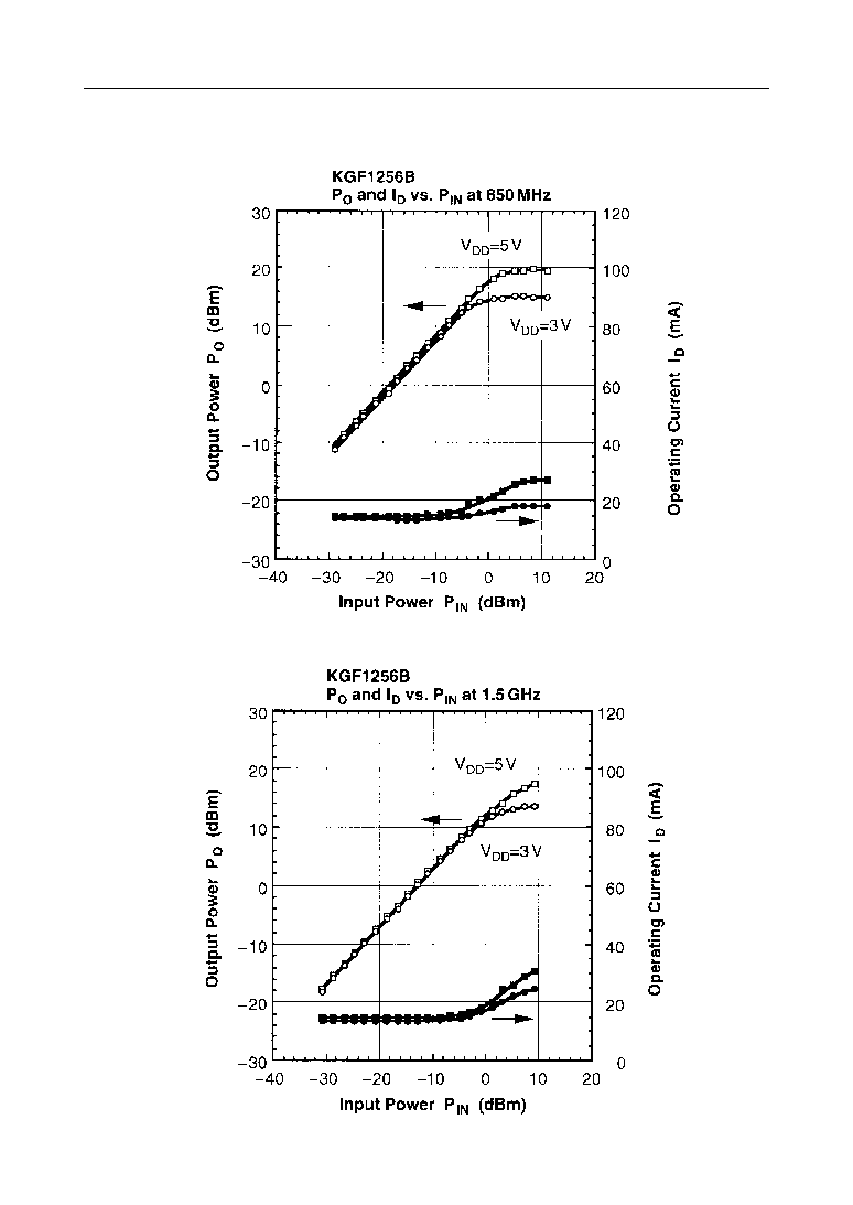
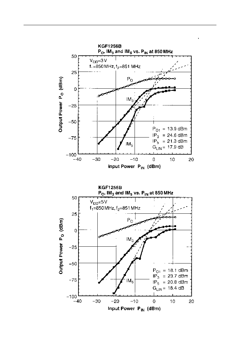
f = 850 MHz
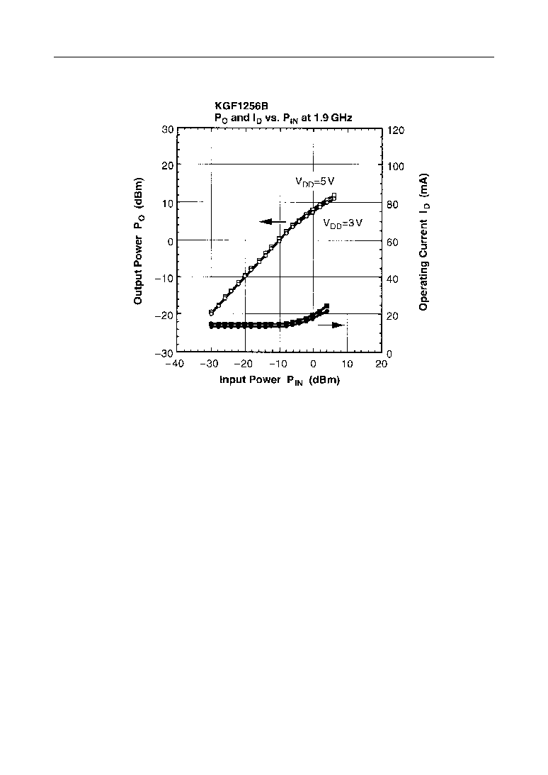
f = 1.9 GHz
f = 850 MHz
f = 1.5 GHz
f = 1.5 GHz
f = 1.9 GHz
f = 850 MHz
f = 1.5 GHz
f = 1.9 GHz
f = 850 MHz
f = 1.5 GHz
f = 1.9 GHz
(Ta = 25∞C)
I
GDO
Gate-drain leakage current
360
mA
--
V
GD
= ≠11 V
--
I
DS(off)
Drain-source leakage current
720
mA
--
V
DS
= 3 V, V
GS
= ≠2 V
--
I
DSS
Drain current
--
mA
100
V
DS
= 3 V, V
GS
= 0 V
--
I
D
Operating current
40.0
mA
--
(*1), P
IN
= 5 dBm,
f = 850 MHz
--
V
GS(off)
Gate-source cut-off voltage
≠0.5
V
≠1.5
V
DS
= 3 V, I
DS
= 720
mA
--
gm
Transconductance
--
mS
100
V
DS
= 3 V, I
DS
= 25 mA
--
F
Noise figure
2.5
dB
--
(*1), f = 850 MHz
--
4/14
KGF1256B/1256
° electronic components
RF CHARACTERISTICS
5/14
KGF1256B/1256
° electronic components
6/14
KGF1256B/1256
° electronic components

7/14
KGF1256B/1256
° electronic components

8/14
KGF1256B/1256
° electronic components

9/14
KGF1256B/1256
° electronic components
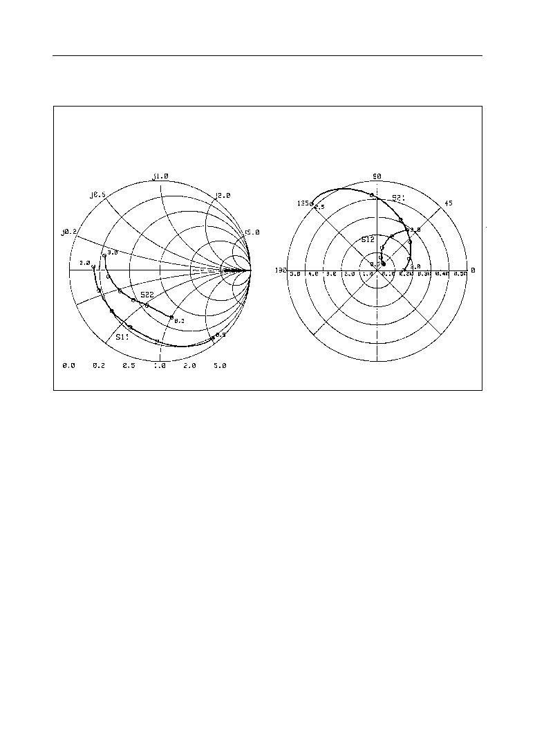
Typical S Parameters of KGF1256B
Freq(MHz)
500.0
MAG(S
11
) ANG(S
11
) MAG(S
21
) ANG(S
21
) MAG(S
12
) ANG(S
12
) MAG(S
22
) ANG(S
22
)
V
DD
= 3 V, V
G
= 0 V, I
D
= 14.0 mA
600.0
700.0
800.0
900.0
1000.0
1100.0
1200.0
1300.0
1400.0
1500.0
1600.0
1700.0
1800.0
1900.0
2000.0
2100.0
2200.0
2300.0
2400.0
2500.0
2600.0
2700.0
2800.0
2900.0
3000.0
0.941
0.917
0.874
0.837
0.806
0.777
0.755
0.737
0.720
0.710
0.703
0.700
0.693
0.691
0.696
0.693
0.693
0.695
0.704
0.702
0.707
0.716
0.719
0.719
0.727
0.731
≠52.03
≠62.43
≠71.90
≠78.93
≠86.02
≠92.27
≠98.15
≠102.90
≠108.50
≠113.18
≠117.55
≠122.22
≠126.28
≠131.15
≠135.24
≠139.61
≠144.32
≠147.69
≠152.62
≠156.91
≠161.26
≠165.51
≠170.07
≠174.51
≠178.84
177.05
5.226
5.315
5.111
4.827
4.537
4.238
3.966
3.730
3.496
3.307
3.145
2.968
2.830
2.672
2.559
2.432
2.310
2.205
2.092
2.006
1.898
1.816
1.732
1.646
1.561
1.492
134.33
126.90
117.12
101.30
94.02
87.45
81.35
75.71
70.03
65.11
59.63
55.27
51.43
40.78
36.30
32.02
27.18
23.36
19.63
15.30
11.81
8.05
4.42
0.51
0.051
0.052
0.050
0.048
0.051
0.052
0.052
0.057
0.061
0.066
0.077
0.082
0.093
0.104
0.115
0.131
0.146
0.159
0.174
0.194
0.210
0.223
0.243
0.253
0.269
0.283
42.22
39.67
38.92
43.95
44.67
52.24
54.10
61.31
68.35
68.45
73.21
74.54
76.69
76.81
78.98
77.39
77.41
73.86
73.40
70.69
66.14
65.02
61.54
58.95
56.33
53.45
0.531
0.470
0.443
0.426
0.415
0.412
0.407
0.412
0.413
0.428
0.435
0.446
0.454
0.461
0.481
0.494
0.500
0.520
0.534
0.547
0.570
0.576
0.597
0.607
0.614
0.630
≠76.18
≠86.88
≠94.46
≠99.94
≠105.46
≠109.85
≠114.89
≠118.94
≠123.38
≠127.26
≠131.30
≠136.06
≠139.61
≠143.33
≠147.66
≠151.56
≠156.02
≠160.73
≠164.01
≠169.05
≠172.95
≠177.32
178.74
174.30
169.67
165.37
45.44
108.84
10/14
KGF1256B/1256
° electronic components
Typical S Parameters of KGF1256B
V
DD
= 3 V, V
G
= 0 V, I
D
= 14.0 mA
Frequency : 0.5 to 3.0 GHz
Z
0
= 50 W

11/14
KGF1256B/1256
° electronic components
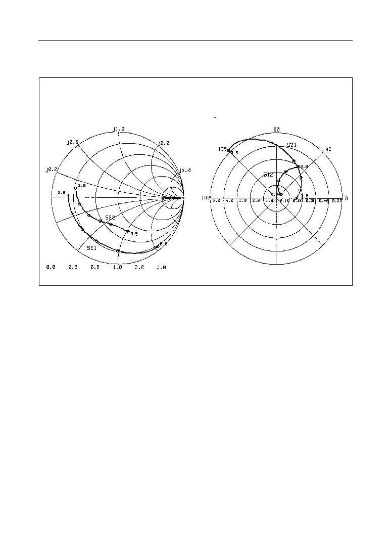
Typical S Parameters of KGF1256B
Freq(MHz)
500.0
MAG(S
11
) ANG(S
11
) MAG(S
21
) ANG(S
21
) MAG(S
12
) ANG(S
12
) MAG(S
22
) ANG(S
22
)
V
DD
= 5 V, V
G
= 0 V, I
D
= 15.4 mA
600.0
700.0
800.0
900.0
1000.0
1100.0
1200.0
1300.0
1400.0
1500.0
1600.0
1700.0
1800.0
1900.0
2000.0
2100.0
2200.0
2300.0
2400.0
2500.0
2600.0
2700.0
2800.0
2900.0
3000.0
0.946
0.929
0.888
0.849
0.819
0.798
0.772
0.754
0.737
0.734
0.725
0.719
0.714
0.712
0.720
0.715
0.716
0.720
0.726
0.726
0.730
0.736
0.742
0.742
0.746
0.753
≠50.39
≠60.59
≠69.71
≠77.00
≠83.83
≠90.00
≠95.94
≠101.07
≠106.32
≠111.29
≠115.68
≠120.16
≠124.65
≠129.15
≠133.48
≠137.90
≠142.76
≠146.59
≠151.65
≠155.82
≠160.35
≠164.80
≠169.18
≠173.83
≠178.20
177.40
5.163
5.261
5.067
4.808
4.532
4.249
3.991
3.747
3.514
3.326
3.174
2.997
2.860
2.700
2.585
2.467
2.331
2.229
2.108
2.017
1.907
1.825
1.734
1.648
1.566
1.494
134.98
127.92
109.79
102.16
94.87
88.30
81.91
76.24
70.45
65.44
59.74
55.18
45.17
40.55
35.99
31.65
26.60
22.47
19.12
10.62
7.08
3.43
≠0.62
0.046
0.044
0.043
0.043
0.045
0.044
0.045
0.052
0.057
0.066
0.074
0.082
0.096
0.106
0.117
0.136
0.151
0.165
0.184
0.202
0.218
0.237
0.252
0.267
0.285
0.296
41.95
42.66
43.75
47.27
46.06
60.51
62.09
68.42
76.71
76.64
81.63
84.47
85.33
81.95
83.83
82.48
83.14
78.59
76.66
75.03
71.03
67.89
64.26
60.87
57.36
55.75
0.531
0.469
0.439
0.426
0.420
0.414
0.407
0.414
0.424
0.437
0.442
0.451
0.460
0.475
0.490
0.509
0.517
0.539
0.551
0.563
0.583
0.595
0.611
0.623
0.632
0.648
≠72.83
≠82.56
≠89.70
≠94.94
≠99.99
≠104.80
≠109.30
≠113.96
≠118.19
≠122.15
≠126.67
≠131.24
≠134.86
≠138.98
≠143.98
≠147.62
≠152.36
≠156.77
≠160.66
≠165.98
≠169.93
≠174.37
≠179.30
176.68
171.64
167.22
50.32
118.20
14.31
12/14
KGF1256B/1256
° electronic components
Typical S Parameters of KGF1256B
V
DD
= 5 V, V
G
= 0 V, I
D
= 15.4 mA
Frequency : 0.5 to 3.0 GHz
Z
0
= 50 W
13/14
KGF1256B/1256
° electronic components
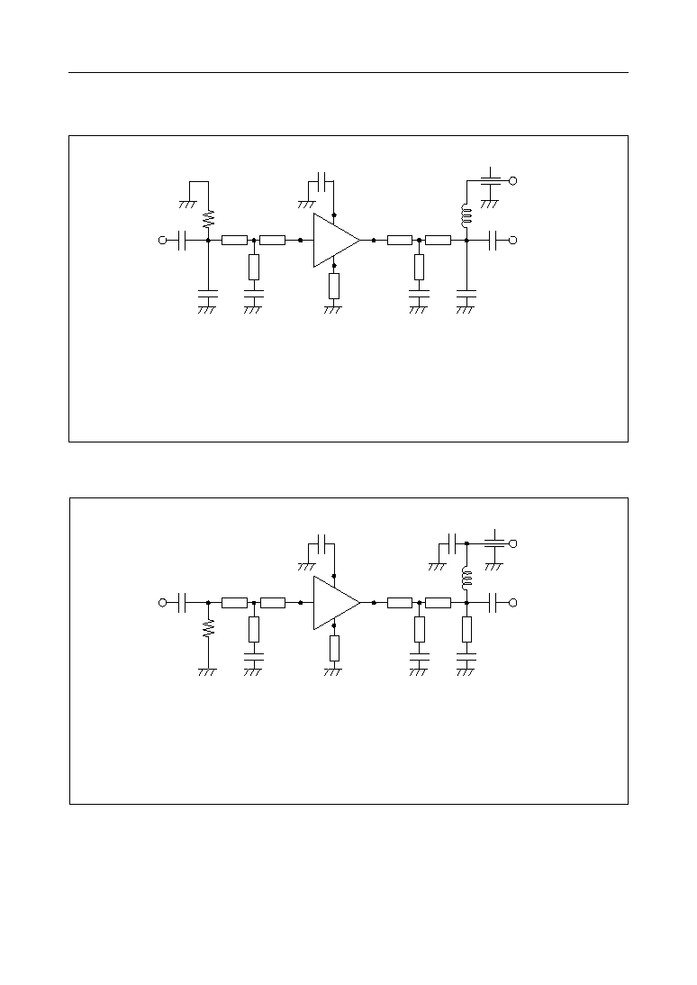
Test Circuit and Bias Configuration for KGF1256B at 1.5 GHz
Test Circuit and Bias Configuration for KGF1256B at 850 MHz
IN
T
1
: Z
0
= 75
W, E = 30 deg
T
2
: Z
0
= 75
W, E = 28 deg
T
3
= T
6
: Z
0
= 100
W, E = 5 deg
C
1
= 7.0 pF, C
2
= 0.8 pF, C
3
= 5.0 pF, C
4
= 5.5 pF, C
S
= 100 pF
C
C(DC Block)
= 1000 pF, C
F(Feed through)
= 1000 pF
RFC = 200 nH, R
G
= 1000
W
OUT
(1)
(3)
(2)
(4)
KGF
1256B
R
G
C
C
T
2
T
1
C
1
C
S
T
5
T
4
C
4
C
C
C
F
V
DD
RFC
T
4
: Z
0
= 75
W, E = 30 deg
T
5
: Z
0
= 75
W, E = 30 deg
T
7
: Z
0
= 100
W, E = 1 deg
T
3
C
2
T
7
T
6
C
3
IN
T
1
: Z
0
= 75
W, E = 65 deg
T
2
: Z
0
= 75
W, E = 40 deg
T
3
= T
6
= T
7
: Z
0
= 100
W, E = 8 deg
C
1
= 2.4 pF, C
2
= 1.2 pF, C
3
= 0.6 pF, C
S
= 100 pF
C
C(DC Block)
= 1000 pF, C
B(By-pass)
= 1000 pF, C
F(Feed through)
= 1000 pF
RFC = 60 nH, R
G
= 1000
W
OUT
(1)
(3)
(2)
(4)
KGF
1256B
R
G
C
C
T
2
T
1
C
S
T
5
T
4
C
3
C
C
V
DD
RFC
T
4
: Z
0
= 75
W, E = 50 deg
T
5
: Z
0
= 75
W, E = 50 deg
T
8
: Z
0
= 100
W, E = 1 deg
T
3
C
1
T
8
T
6
C
2
T
7
C
B
C
F

14/14
KGF1256B/1256
° electronic components
Test Circuit and Bias Configuration for KGF1256B at 1.9 GHz
IN
T
1
: Z
0
= 75
W, E = 65 deg
T
2
: Z
0
= 75
W, E = 40 deg
T
3
= T
6
= T
7
: Z
0
= 100
W, E = 1 deg
C
1
= 1.7 pF, C
2
= 1.3 pF, C
3
= 0.2 pF, C
S
= 100 pF
C
C(DC Block)
= 1000 pF, C
B(By-pass)
= 1000 pF, C
F(Feed through)
= 1000 pF
RFC = 60 nH, R
G
= 1000
W
OUT
(1)
(3)
(2)
(4)
KGF
1256B
R
G
C
C
T
2
T
1
C
S
T
5
T
4
C
3
C
C
V
DD
RFC
T
4
: Z
0
= 75
W, E = 50 deg
T
5
: Z
0
= 75
W, E = 50 deg
T
8
: Z
0
= 100
W, E = 1 deg
T
3
C
1
T
8
T
6
C
2
T
7
C
B
C
F