 | –≠–ª–µ–∫—Ç—Ä–æ–Ω–Ω—ã–π –∫–æ–º–ø–æ–Ω–µ–Ω—Ç: KGL4175HW | –°–∫–∞—á–∞—Ç—å:  PDF PDF  ZIP ZIP |
1Electronic Components
September 9, 2002
GTD-18609 Rev. 1.1
KGL4175HW
Preliminary
10.7 Gbps Direct Modulation Driver IC
1/6
FEATURES
∑ Low Power
: 0.6 W (excluding modulation current and bias current)
∑ High Sensitive Input
: 0.25 Vpp (differential)
∑ Modulation Current Control
: 20 mApp to 50 mApp
∑ Bias Current Control
: 0 mA to 45 mA
∑ X-Point Controllability
: 40 % to 60 %
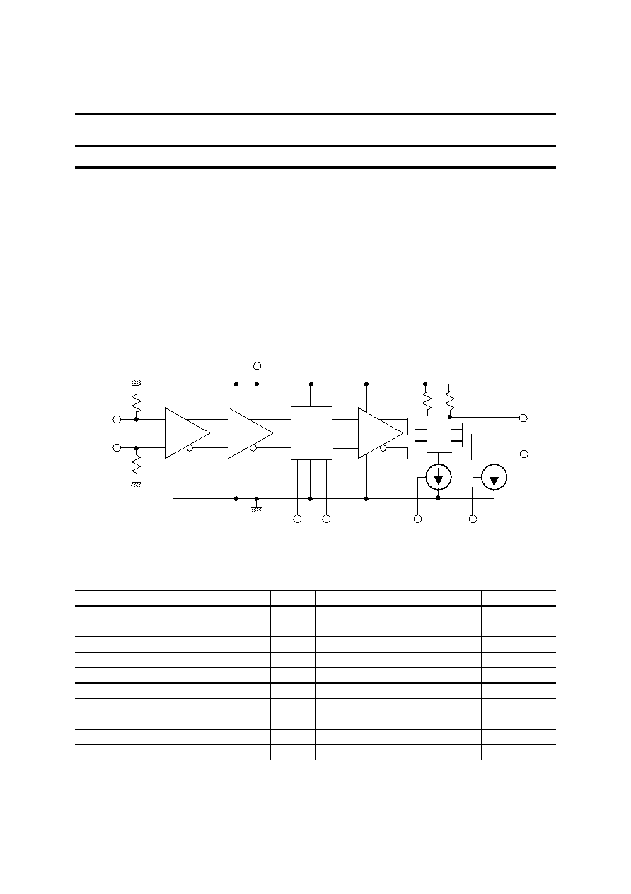
FUNCTION DIAGRAM
ABSOLUTE MAXIMUM RATINGS
Parameter
Symbol
Min
Max
Unit
Note
Supply Voltage
VD1
-0.3
4
V
Voltage of Modulation Current Output
V(OUT)
-0.3
6
V
Voltage of Bias Current Output
V(BIAS)
-0.3
6
V
X-Point Control Voltage
VB1
-1
+2.5
V
X-Point Reference Voltage
VB2
-1
+2.5
V
Modulation Current Control Voltage
VC1
-1
+1.6
V
Bias Current Control Voltage
VC2
-1
+2.6
V
Input Amplitude
Vin
-
1.6
Vpp
AC coupled
Operating Temperature at Package Base
Ts
-10
100
∞C
Storage Temperature
Tst
-40
125
∞C
IN
INB
OUT
Crossing
Point
Control
VD1
VB1
VB2
VC1
VC2
BIAS
150
50
50

GTD-18609 Rev. 1.1
1Electronic Components
KGL4175HW
2/6
RECOMMENDED OPERATING CONDITIONS
Parameter
Symbol
Min
Typ
Max
Unit
Note
Supply Voltage
VD1
3.13
3.3
3.47
V
Low Voltage of Modulation Current Output
VL(OUT)
1.4
-
-
V
Low Voltage of Bias Current Output
VL(BIAS)
1.9
-
-
V
X-Point Control Voltage
VB1
0.6
1.2
1.8
V
X-Point Reference Voltage
VB2
1)
1.2
V
Output Amplitude Control Voltage
VC1
0
-
1.2
V
Output Bias Control Voltage
VC2
0
-
2.4
V
Single-ended Input Amplitude
0.5
-
1.2
Vpp
AC coupled
Differential Input Amplitude
Vin
0.25
-
1.2
Vpp
AC coupled
Operating Temperature at Package Base
Ts
0
-
85
∞C
Input Interface
AC coupled (External blocking capacitor is required)
Output Interface
DC coupled( Pull up through LD )
1) VB2 can be open or biased by the external circuit.
For VB2 opened, VB2 is biased at about 1.2V ( VD1=3.3V ).
ELECTRICAL CHARACTERISTICS ( TARGET SPECIFICATIONS)
Parameter
Symbol
Condition
Min
Typ
Max
Unit
Maximum Operating Data Rate
NRZ
10.7
-
-
Gbps
Supply Current
Id1
-
150
180
mA
Minimum Modulation Current
Imod (min)
50
load
-
20
25
mApp
Maximum Modulation Current
Imod (max)
50
load
45
50
-
mApp
Minimum Bias Current
Ibias (min)
50
load
-
0
0.5
mA
Maximum Bias Current
Ibias (max)
50
load
40
45
-
mA
High
XPH
57
60
%
X-Point Control Range
Low
XPL
50
load,
NRZ
-
40
43
%
X-Point Stability
Del (Xp)
50
load,
0≠85∞C
-10
-
10
%
Output Rise/Fall Time
Tr/Tf
50
load,
20%/80%
-
25
37
ps
Input Return Loss
S11
100kHz≠10 GHz
-
13
-
dB
GTD-18609 Rev. 1.1
1Electronic Components
KGL4175HW
3/6
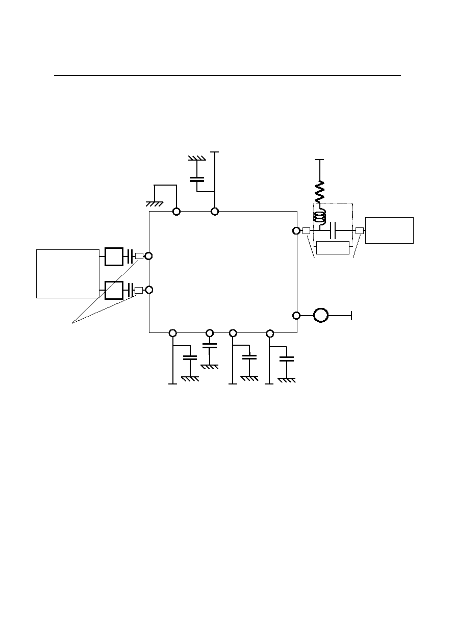
AC CHARACTERISTICS TEST CIRCUIT
IN
OUT
GND
Blocking
Capacitor
0.1
µ
F
P
o
w
e
r
S
uppl
y
(VD1
)
VB1
KGL4175HW
INB
VB2
VD1
VC1
VC2
+3.
8
V
BIAS
0.1
µ
F
Bias-T
50
OSCILLO
-SCOPE
PULSE
PATTERN
GENERATOR
Fc=7.5GHz
Bessel
Filter
P
o
w
e
r
S
uppl
y
(VB
1
)
P
o
w
e
r
S
uppl
y
(VC
1
)
P
o
w
e
r
S
uppl
y
(VC
2
)
+3.8V
I
BIAS
0.1
µ
F
0.1
µ
F
0.1
µ
F
50
Transmission Line
50
Transmission Line

GTD-18609 Rev. 1.1
1Electronic Components
KGL4175HW
4/6
PACKAGE DIMENSIONS
Note. This package is non-hermetic.
PIN CONNECTION
No.
Symbol
Note
1
GND
Ground
2
GND
Ground
3
GND
Ground
4
GND
Ground
5
GND
Ground
6
GND
Ground
7
BIAS
Bias Current Output Port
8
GND
Ground
9
GND
Ground
10
OUT
Modulation Current Output Port
11
GND
Ground
12
GND
Ground
13
GND
Ground
14
GND
Ground
15
GND
Ground
16
GND
Ground
17
GND
Ground
18
VC2
Bias Current Control Port
19
VC1
Modulation Current Control Port
20
VD1
Supply Voltage Port
21
VD1
Supply Voltage Port
22
VB2
X-Point Reference Port
23
VB1
X-Point Control Port
24
GND
Ground
25
GND
Ground
26
GND
Ground
27
GND
Ground
28
INB
Inverted Input Port
29
GND
Ground
30
GND
Ground
31
IN
Signal Input Port
32
GND
Ground
4.445
(Lot No.)
Unit : mm
(T
op View)
28-0.635
7.0±
0.2
7.0±0.2
25
32
24 17
16
9
1.5±0.25
1 8
K4175
1
HW
0.4
0.1
2
5
0.6
2
0.5
0.3
5
GTD-18609 Rev. 1.1
1Electronic Components
KGL4175HW
5/6
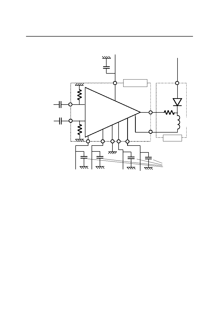
TYPICAL APPLICATION
APPLICATION NOTE
1. For stable operation;
1-1. To prevent a dependence of "X-Point" on the supply voltage VD1,
(1) Use an external voltage source of 1.2V for "VB2", or
(2) Control the voltage of "VB1", so that the voltage difference "VB1≠VB2" is constant.
2. Power-up/shut-down sequence;
For power-up, LD pull up voltage at first, next supply voltage(VD1), then control voltages (VB1, VB2,
VC1, VC2) or supply all simultaneously.
For shut-down, control voltages at first, next VD1 then LD pull up voltage or shut down all
simultaneously. .
Customer does not need to care about the sequence for the control voltages (VB1,VB2,VC1,VC2).
Ou
tp
ut
B
i
a
s
Co
ntr
o
l
Data Input
IN
OUT
GND
Blocking
Capacitor
Ex. 0.1
µ
F
Chip
Capacitor
0.1
µ
F
S
u
pp
ly
V
o
lt
a
g
e
Ou
tp
ut
A
m
p
litud
e
X
-
P
o
int Re
f
e
r
e
nce
VB1
KGL4175HW
LD Module
X
-
P
o
int Co
n
t
r
o
l
Data-bar Input
INB
VB2
VD1
VC1
VC2
P
u
ll
Up
BIAS
Choke
Coil
Chip
Capacitor
0.1
µ
F

GTD-18609 Rev. 1.1
1Electronic Components
KGL4175HW
6/6
SAFETY AND HANDRING INFORMATION ON GaAs DEVICES
Arsenic Compound (GaAs Devices)
The product contains arsenic (As) as a compound.
This material is stable for normal use, however, its dust or vapor may be potentially hazardous to the human
body.
Avoid ingestion, fracture, burning or chemical treatment to the product.
∑ Do not put the product in your mouth.
∑ Do not burn or destroy the product.
∑ Do not perform chemical treatment for the product.
Keep laws and ordinances related to the disposal of the products.
NOTICE
1.
The information contained herein can change without notice owing to product and/or technical improvements.
Before using the product, please make sure that the information being referred to is up-to-date.
2.
The outline of action and examples for application circuits described herein have been chosen as an
explanation for the standard action and performance of the product. When planning to use the product, please
ensure that the external conditions are reflected in the actual circuit, assembly, and program designs.
3.
When designing your product, please use our product below the specified maximum ratings and within the
specified operating ranges including, but not limited to, operating voltage, power dissipation, and operating
temperature.
4.
Oki assumes no responsibility or liability whatsoever for any failure or unusual or unexpected operation
resulting from misuse, neglect, improper installation, repair, alteration or accident, improper handling, or
unusual physical or electrical stress including, but not limited to, exposure to parameters beyond the specified
maximum ratings or operation outside the specified operating range.
5.
Neither indemnity against nor license of a third party's industrial and intellectual property right, etc. is
granted by us in connection with the use of the product and/or the information and drawings contained herein.
No responsibility is assumed by us for any infringement of a third party's right which may result from the use
thereof.
6.
The products listed in this document are intended for use in general electronics equipment for commercial
applications (e.g., office automation, communication equipment, measurement equipment, consumer
electronics, etc.). These products are not authorized for use in any system or application that requires special
or enhanced quality and reliability characteristics nor in any system or application where the failure of such
system or application may result in the loss or damage of property, or death or injury to humans.
Such applications include, but are not limited to, traffic and automotive equipment, safety devices, aerospace
equipment, nuclear power control, medical equipment, and life-support systems.
7.
Certain products in this document may need government approval before they can be exported to particular
countries. The purchaser assumes the responsibility of determining the legality of export of these products
and will take appropriate and necessary steps at their own expense for these.
8.
No part of the contents contained herein may be reprinted or reproduced without our prior permission.
Copyright 2002 Oki Electric Industry Co., Ltd.