1
Oki Semiconductor
KGL4216
10-Gbps GaAs T-Flip Flop IC
INTRODUCTION
Oki Semiconductor's KGL4216 is a 10-Gbps T-Flip Flop IC designed for ultra high-speed digital
communications systems. The KGL4216 uses 0.2-µm gate length GaAs MESFETs and Oki's unique MCFF
( Memory Cell type Flip Flop ) technology to achieve operations of over 11-GHz. The KGL4216 is
available as a 24-pin ceramic packaged device. Due to the KGL4216's high sensitivity, capacitive
coupling is recommended for the KGL4216's I/O connections.
FEATURES
∑ High-speed operation: 11-Gbps data rate (min)
∑ Low-power dissipation: 400 mW (typ.) using 2-V power-supply
∑ 0.2-µm gate length GaAs MESFET process
∑ MCFF ( Memory Cell type Flip Flop ) technology
∑ 24-pin ceramic package
APPLICATION
∑ High-speed optical communication systems: 10 Gbps
∑ High-speed test equipment
s
KGL4216
s
≠≠≠≠≠≠≠≠≠≠≠≠≠≠≠≠≠≠≠≠≠≠≠≠≠≠≠≠≠≠≠≠≠≠≠≠≠≠≠≠≠≠≠≠≠≠≠≠≠≠≠≠≠≠≠≠≠≠≠≠≠≠≠≠≠≠≠≠≠≠≠≠≠≠≠≠≠≠≠≠≠≠≠
2
Oki Semiconductor
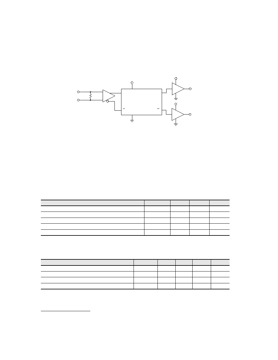
BLOCK DIAGRAM
ELECTRICAL CHARACTERISTICS
Exceeding these maximum ratings could cause immediate damage or lead to permanent deterioration of the device.
Absolute Maximum Ratings
Parameter
Symbol
Min.
Max.
Units
Supply Voltage
V
DD
-0.3
2.3
V
Clock Input Voltage
V
CI
-0.3
1.5
V
Clock Reference Bias Voltage
V
RI
-0.3
1.5
V
Temperature at Package Base under Bias
Ts
-45
100
∞C
Storage Temperature
Tst
-45
125
∞C
Electrical Characteristics
V
DD
= 2 V ± 0.1 V, Ts = 0∞C to 70∞C
Parameter
Symbol
Min.
Typ.
Max.
Units
Maximum Operating Frequency Range
OFR
11
GHz
Power Dissipation
PW
0.4
0.5
W
Clock Input Voltage Swing
V
I
0.3
0.8
1.2
Vpp
Output Voltage Swing
V
O
0.4
0.6
0.8
Vpp
CR
CK
50
QN
V
DD
V
DD
CK
Clock Input Terminal
CR
Reference Voltage Bias Terminal
Q, QN
Complimentary Data Outputs
VDD
Power Supply of Internal Circuit
Q
V
DD
C
C
Q
Q
T-Flip Flop
(MCFF)