Document Outline
- DESCRIPTION
- FEATURES
- PRODUCT FAMILY
- PIN CONFIGURATION (TOP VIEW)
- PIN DESCRIPTION
- BLOCK DIAGRAM
- ELECTRICAL CHARACTERISTICS
- TIMING CHART
- Read & Write Cycle (Same Bank) @CAS Latency = 2, Burst Length = 4
- Single Bit Read-Write-Read Cycle (Same Page) @CAS Latency = 2, Burst Length = 4
- Page Read & Write Cycle (Same Bank) @CAS Latency = 2, Burst Length = 4
- Burst Read & Single Write Cycle (Same Bank) @CAS Latency = 2, Burst Length = 4
- Read & Write Cycle with Auto Precharge @ Burst Length = 4
- Bank Interleave Random Row Read Cycle @CAS Latency = 2, Burst Length = 4
- Bank Interleave Random Row Write Cycle @CAS Latency = 2, Burst Length = 4
- Bank Interleave Page Read Cycle @CAS Latency = 2, Burst Length = 4
- Bank Interleave Page Write Cycle @CAS Latency = 2, Burst Length = 4
- Bank Interleave Random Row Read/Write Cycle @CAS Latency = 2, Burst Length = 4
- Bank Interleave Page Read/Write Cycle @CAS Latency = 2, Burst Length = 4
- Clock Suspension & DQM Operation Cycle @CAS Latency = 2, Burst Length = 4
- Read to Write Cycle (Same Bank) @CAS Latency = 2, Burst Length = 4
- Read Interruption by Precharge Command @Burst Length = 8
- Burst Stop Command @Burst Length = 8
- Power Down Mode @CAS Latency = 2, Burst Length = 4
- Self Refresh Cycle
- Mode Register Set Cycle Auto Refresh Cycle
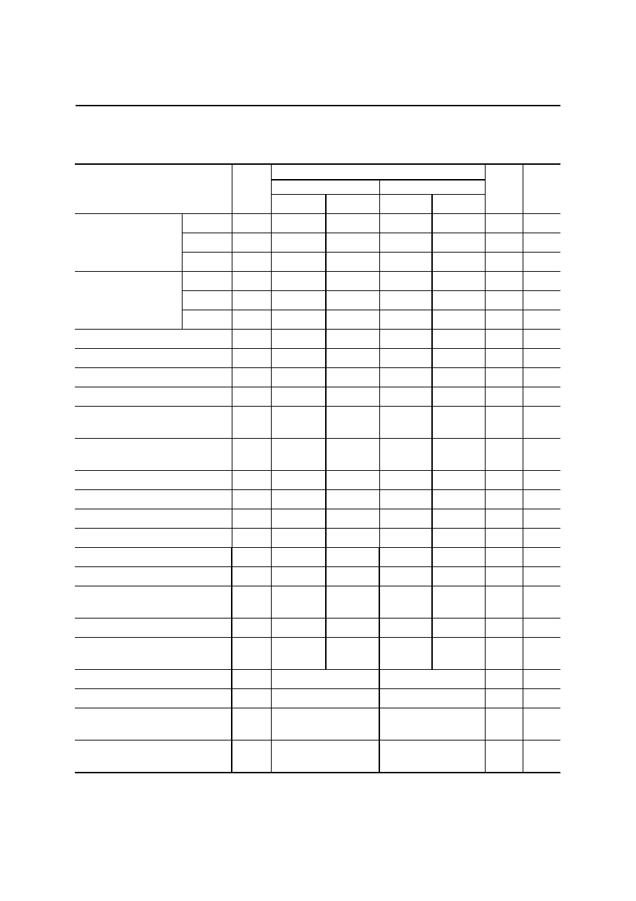
- FUNCTION TRUTH TABLE (Table 1) (1/2)
- FUNCTION TRUTH TABLE (Table 1) (2/2)
- FUNCTION TRUTH TABLE for CKE (Table 2)
- PACKAGE DIMENSIONS
- REVISION HISTORY

OKI Semiconductor
FEDD56V62160E-01
Issue Date: Feb. 4, 2002
MD56V62160E
4-Bank
�
1,048,576-Word
�
16-Bit SYNCHRONOUS DYNAMIC RAM
1/34
DESCRIPTION
The MD56V62160E is a 4-Bank
�
1,048,576-word
�
16-bit Synchronous dynamic RAM fabricated in
Oki's silicon-gate CMOS technology. The device operates at 3.3 V. The inputs and outputs are LVTTL
compatible.
FEATURES
�
Silicon gate, quadruple polysilicon CMOS, 1-transistor memory cell
� 4-Bank
�
1,048,576-word
�
16-bit configuration
�
Single 3.3 V power supply,
�
0.3 V tolerance
�
Input : LVTTL compatible
�
Output : LVTTL compatible
�
Refresh : 4096 cycles/64 ms
�
Programmable data transfer mode
- CAS Latency (1, 2, 3)
- Burst Length (1, 2, 4, 8, Full Page)
- Data scramble (sequential, interleave)
�
CBR auto-refresh, Self-refresh capability
� Packages:
54-pin 400 mil plastic TSOP (TypeII)
(
TSOP(2)54-P-400-0.80-K
)
(Product: MD56V62160E-xxTA)
xx indicates speed rank.
PRODUCT FAMILY
Access Time (Max.)
Family
Max.
Frequency
t
AC2
t
AC3
MD56V62160E-7
143 MHz
6 ns
6 ns
MD56V62160E-10
100 MHz
6 ns
6 ns

FEDD56V62160E-01
OKI Semiconductor
MD56V62160E
2/34
PIN CONFIGURATION (TOP VIEW)
Pin Name
Function
Pin Name
Function
CLK
System Clock
UDQM, LDQM
Data Input/ Output Mask
CS
Chip Select
DQi
Data Input/ Output
CKE Clock
Enable V
CC
Power Supply (3.3 V)
A0�A10 Address V
SS
Ground (0 V)
A11 Bank
Select
Address V
CC
Q
Data Output Power Supply (3.3 V)
RAS
Row Address Strobe
V
SS
Q
Data Output Ground (0 V)
CAS
Column Address Strobe
NC
No Connection
WE
Write Enable
Note : The same power supply voltage must be provided to every V
CC
pin and V
CC
Q pin.
The same GND voltage level must be provided to every V
SS
pin and V
SS
Q pin.
54-Pin Plastic TSOP(II)
(K Type)
1
2
3
4
5
9
10
11
12
13
54
53
52
51
50
46
45
44
43
42
DQ1
V
CC
Q
DQ3
V
CC
V
SS
DQ16
V
SS
Q
DQ14
V
SS
Q
V
CC
Q
DQ7
V
SS
Q
DQ8
DQ10
V
CC
Q
NC
6
7
8
14
15
DQ5
CAS
V
CC
V
SS
Q
19
20
21
22
23
A12
A10
A0
A1
CS
16
17
18
24
25
RAS
LDQM
A13
WE
49
48
47
V
CC
Q
DQ12
41
40
36
35
34
33
32
V
SS
NC
A11
A9
A8
A7
A6
39
38
37
UDQM
CLK
CKE
31
30 A5
A2
DQ6
DQ4
DQ2
DQ15
DQ13
DQ11
DQ9
A3 26
27
A4
29
28 V
SS
V
CC

FEDD56V62160E-01
OKI Semiconductor
MD56V62160E
3/34
PIN DESCRIPTION
CLK
Fetches all inputs at the "H" edge.
CS
Disables or enables device operation by asserting or deactivating all inputs except CLK, CKE,
UDQM and LDQM.
CKE
Masks system clock to deactivate the subsequent CLK operation.
If CKE is deactivated, system clock will be masked so that the subsequent CLK operation is
deactivated. CKE should be asserted at least one cycle prior to a new command.
Address
Row & column multiplexed.
Row address
: RA0 � RA11
Column Address
: CA0 � CA7
A13, A12
(BA0, BA1)
Slects bank to be activated during row address latch time and selects bank for precharge and
read/write during column address latch time.
RAS
CAS
WE
Functionality depends on the combination. For details, see the function truth table.
UDQM,
LDQM
Masks the read data of two clocks later when UDQM and LDQM are set "H" at the "H" edge of the
clock signal. Masks the write data of the same clock when UDQM and LDQM are set "H" at the "H"
edge of the clock signal. UDQM controls upper byte and LDQM controls lower byte.
DQi
Data inputs/outputs are multiplexed on the same pin.

FEDD56V62160E-01
OKI Semiconductor
MD56V62160E
4/34
BLOCK DIAGRAM
Timing
Register
Column
Decoders
Sense
Amplifiers
DQ1 -
DQ16
RAS
CAS
A0 - A11
Progra-m
ing
Register
Bank
Controller
Latency
& Burst
Controller
Internal
Col.
Address
Counter
I/O
Controller
Column
Address
Buffers
Internal
Row
Address
Counter
Row
Address
Buffers
8
Row
Decoders
Word
Drivers
16Mb
Memory
Cells
Read
Data
Register
Output
Buffers
Column
Decoders
Input
Data
Register
Input
Buffers
CKE
CLK
CS
WE
UDQM
LDQM
A13, A12
8
12
16
16
16
16
Row
Decoders
Word
Drivers
16Mb
Memory
Cells
8
Column
Decoders
Row
Decoders
Word
Drivers
16Mb
Memory
Cells
Column
Decoders
Row
Decoders
Word
Drivers
16Mb
Memory
Cells
12
12
12
12
8
8
8
16
Sense
Amplifiers
Sense
Amplifiers
Sense
Amplifiers
8

FEDD56V62160E-01
OKI Semiconductor
MD56V62160E
5/34
ELECTRICAL CHARACTERISTICS
Absolute Maximum Ratings
Parameter Symbol
Value
Unit
Voltage on Any Pin Relative to V
SS
V
IN
, V
OUT
�0.5 to V
CC
+ 0.5
V
V
CC
Supply Voltage
V
CC
, V
CC
Q
�0.5 to 4.6
V
Storage Temperature
T
stg
�55 to 150
�C
Power Dissipation
P
D*
1000
mW
Short Circuit Output Current
I
OS
50
mA
Operating Temperature
T
opr
0 to 70
�C
*: Ta = 25
�
C
Recommended Operating Conditions
(Voltages referenced to V
SS
= 0 V)
Parameter Symbol
Min.
Typ.
Max.
Unit
Power Supply Voltage
V
CC
, V
CC
Q 3.0
3.3
3.6
V
Input High Voltage
V
IH
2.0
V
CC
+ 0.3
V
Input Low Voltage
V
IL
-
0.3
0.8 V
Pin Capacitance
(V
bias
= 1.4 V, Ta = 25�C, f = 1 MHz)
Parameter Symbol
Min.
Max.
Unit
Input Capacitance (CLK)
C
CLK
2.5 4 pF
Input Capacitance
(
RAS
,
CAS
,
WE
,
CS
, CKE, UDQM, LDQM,
A0 - A13)
C
IN
2.5 5 pF
Input/Output Capacitance (DQ1 � DQ16)
C
OUT
4 6.5
pF

FEDD56V62160E-01
OKI Semiconductor
MD56V62160E
6/34
DC Characteristics
MD56V62160
Condition
E-7 E-10
Parameter
Symbol
Bank CKE Others
Min. Max. Min. Max.
Unit Note
Output High
Voltage
V
OH
I
OH
=
-
2.0mA
2.4
2.4
V
Output Low
Voltage
V
OL
I
OL
=
2.0mA
0.4
0.4 V
Input Leakage
Current
I
LI
-
10 10
-
10 10
�
A
Output Leakage
Current
I
LO
-
10 10
-
10 10
�
A
I
CC1
One Bank
Active
CKE
V
IH
t
CC
= Min.
t
RC
= Min.
No Burst
85
70
mA
1,2
Average Power
Supply Current
(Operating)
I
CC1D
Both
Banks
Active
CKE
V
IH
t
CC
= Min.
t
RC
= Min.
t
RRD
= Min.
No Burst
135
115
mA
1,2
Power Supply
Current
(Standby)
I
CC2
Both
Banks
Precharge
CKE
V
IH
t
CC
= Min.
30
30
mA
3
Average Power
Supply Current
(Clock
Suspension)
I
CC3S
Both
Banks
Active
CKE
V
IL
t
CC
= Min.
3
3
mA
2
Average Power
Supply Current
(Active Standby)
I
CC3
One Bank
Active
CKE
V
IH
t
CC
= Min.
40
30
mA
3
Power Supply
Current (Burst)
I
CC4
Both
Banks
Active
CKE
V
IH
t
CC
= Min.
110
90
mA
1,2
Power Supply
Current
(Auto-Refresh)
I
CC5
One Bank
Active
CKE
V
IH
t
CC
= Min.
t
RC
= Min.
135
115
mA 2
Average Power
Supply Current
(Self-Refresh)
I
CC6
Both
Banks
Precharge
CKE
V
IL
t
CC
= Min.
2
2
mA
Average Power
Supply Current
(Power Down)
I
CC7
Both
Banks
Precharge
CKE
V
IL
t
CC
= Min.
2
2
mA
Notes: 1. Measured with outputs open.
2. The address and data can be changed once or left unchanged during one cycle.
3. The address and data can be changed once or left unchanged during two cycles. DC

FEDD56V62160E-01
OKI Semiconductor
MD56V62160E
7/34
Mode Set Address Keys
Single Write
CAS
Latency
Burst Type
Burst Length
A9
BRSW
A6 A5 A4
CL
A3
BT
A2 A1 A0
BT = 0
BT = 1
0 Normal 0
0
0
Reserved
0
Sequential
0 0 0
1
1
1
Single
Write
0
0
1 1 1
Interleave
0
0
1 2
2
0 1 0
2
0 1 0
4
4
0 1 1
3
0 1 1
8
8
1 0 0 Reserved
1 0 0 Reserved
Reserved
1 0 1 Reserved
1 0 1 Reserved
Reserved
1 1 0 Reserved
1 1 0 Reserved
Reserved
1 1 1 Reserved
1 1 1 Full
Page
Reserved
Notes: A7, A8, A10, A11, A12 and A13 should stay "L" during mode set cycle.
MD56V62160E supports two methods of Power on Sequence.
POWER ON SEQUENCE 1
1. With inputs in NOP state, turn on the power supply and start the system clock.
2.
After
the
V
CC
voltage has reached the specified level, pause for 200
�
s or more with the input kept in
NOP state.
3. Issue the precharge all bank command.
4. Apply a CBR auto-refresh eight or more times.
5. Enter the mode register setting command.
POWER ON SEQUENCE 2
1. With inputs in NOP state, turn on the power supply and start the system clock.
2.
After
the
V
CC
voltage has reached the specified level, pause for 200
�
s or more with the input kept in
NOP state.
3. Issue the precharge all bank command.
4. Enter the mode register setting command.
5. Apply a CBR auto-refresh eight or more times.
FEDD56V62160E-01
OKI Semiconductor
MD56V62160E
8/34
AC Characteristics (1/2)
Note1, 2
MD56V62160
E-7 E-10
Parameter Symbol
Min. Max. Min. Max.
Unit Note
CL = 3
t
CC3
7
10
ns
CL = 2
t
CC2
10
10
ns
Clock Cycle Time
CL = 1
t
CC1
20
20
ns
CL = 3
t
AC3
6
6
ns 3,
4
CL = 2
t
AC2
6
6
ns 3,
4
Access Time from
Clock
CL = 1
t
CC1
17
17
ns 3,
4
Clock High Pulse Time
t
CH
2
3
ns 4
Clock Low Pulse Time
t
CL
2
3
ns 4
Input Setup Time
t
SI
1.5
3
ns
Input Hold Time
t
HI
0.8
1
ns
Output Low Impedance Time
from Clock
t
OLZ
1
1
ns
Output High Impedance Time
from Clock
t
OHZ
6
6
ns
Output Hold from Clock
t
OH
2
3
ns 3
Random Read or Write Cycle Time
t
RC
69
70
ns
RAS
Precharge Time
t
RP
20
20
ns
RAS
Pulse Width
t
RAS
49 100,000 50 100,000
ns
RAS
to
CAS
Delay Time
t
RCD
20
20
ns
Write Recovery Time
t
WR
8
10
ns
RAS
to
CAS
Bank Active Delay
Time
t
RRD
14
20
ns
Refresh Time
t
REF
64
64
ms
Power-down Exit setup Time
t
RDE
t
SI
+1CLK
t
SI
+1CLK
ns
CAS
to
CAS
Delay Time (Min.)
l
CCD
1
1 Cycle
Clock Disable Time from CKE
l
CKE
1
1 Cycle
Data Output High Impedance Time
from UDQM, LDQM
l
DOZ
2
2 Cycle
Dada Input Mask Time from UDQM,
LDQM
l
DOD
0
0 Cycle

FEDD56V62160E-01
OKI Semiconductor
MD56V62160E
9/34
AC Characteristics (2/2)
Note1, 2
MD56V62160
E-7 E-10
Parameter Symbol
Min. Max. Min. Max.
Unit Note
Data Input Mask Time from Write
Command
l
DWD
0
0 Cycle
Data Output High Impedance Time
from Precharge Command
l
ROH
CL
CL Cycle
Active Command Input Time from
Mode Register Set Command Input
(Min.)
l
MRD
2
2 Cycle
Write Command Input Time from
Output
l
OWD
2
2 Cycle
Notes: 1. AC measurements assume that t
T
= 1 ns.
2. The reference level for timing of input signals is 1.4 V.
The input signal conditions are below.
V
IH
= 2.4 V, V
IL
= 0.4 V
3.
Output
load.
4. The access time is defined at 1.4 V.
5.
If
t
T
is longer than 1 ns, then the reference level for timing of input signals is V
IH
and V
IL
.
Output
Z = 50
50 pF (External Load)

FEDD56V62160E-01
OKI Semiconductor
MD56V62160E
10/34
TIMING CHART
Read & Write Cycle (Same Bank) @
CAS Latency
=
2, Burst Length
=
4
0
1
2
3
4
5
6
7
8
9
10
11
12
13 14
15
16
17
18 19
CLK
CKE
CS
RAS
CAS
ADDR
A12,
A13
A10
DQ
WE
UDQM,
LDQM
t
OH
Ra
Ca0
t
RP
t
RC
Qa1
Cb0
Rb
Rb
Ra
Qa0
Qa2 Qa3
Db0
Db1
Db2
Db3
t
AC
t
OH
Row Active
Read Command
Precharge Command
Row Active
Write Command
Precharge Command
t
RCD

FEDD56V62160E-01
OKI Semiconductor
MD56V62160E
11/34
Single Bit Read-Write-Read Cycle (Same Page) @
CAS Latency
=
2, Burst Length = 4
CLK
CKE
CS
RAS
CAS
ADDR
A12.
A13
A10
DQ
WE
UDQM,
LDQM
Row Active
0
1
2
3
4
5
6
7
8
9
10
11
12
13 14
15
16
17
18 19
High
t
OLZ
Db
t
SI
Qc
t
HI
Qa
t
OH
Ra
l
OWD
BS
BS
BS
BS
BS
Ra
Cc
Cb
Ca
t
OHZ
t
AC
t
HI
t
SI
t
SI
t
HI
t
HI
t
SI
t
SI
t
HI
t
HI
t
SI
I
CCD
t
SI
t
CL
t
CC
t
CH
Read Command
Write Command
Read Command
Precharge Command

FEDD56V62160E-01
OKI Semiconductor
MD56V62160E
12/34
*Notes: 1. When
CS is set "High" at a clock transition from "Low" to "High", all inputs except CLK, CKE,
UDQM and LDQM are invalid.
2. When issuing an active, read or write command, the bank is selected by A12 and A13.
A11
A12
Active, read or write
0 0
Bank
A
0 1
Bank
B
1 0
Bank
C
1 1
Bank
D
3. The auto precharge function is enabled or disabled by the A10 input when the read or write command
is issued.
A10 A12 A13
Operation
0
0
0
After the end of burst, bank A holds the idle status.
1
0
0
After the end of burst, bank A is precharged automatically.
0
0
1
After the end of burst, bank B holds the idle status.
1
0
1
After the end of burst, bank B is precharged automatically.
0
1
0
After the end of burst, bank C holds the idle status.
1
1
0
After the end of burst, bank C is precharged automatically.
0
1
1
After the end of burst, bank D holds the idle status.
1
1
1
After the end of burst, bank D is precharged automatically.
4. When issuing a precharge command, the bank to be precharged is selected by the A10 and A11 inputs.
A10
A12
A13 Operation
0
0
0
Bank A is precharged.
0
0
1
Bank B is precharged.
0
1
0
Bank C is precharged.
0
1
1
Bank D is precharged.
1
X
X
All banks are precharged.
5. The input data and the write command are latched by the same clock (Write latency = 0).
6. The output is forced to high impedance by (1CLK+ t
OHZ
) after UDQM, LDQM entry.

FEDD56V62160E-01
OKI Semiconductor
MD56V62160E
13/34
Page Read & Write Cycle (Same Bank) @
CAS Latency
=
2, Burst Length = 4
*Notes: 1. To write data before a burst read ends, UDQM and LDQM should be asserted three cycles prior to the
write command to avoid bus contention.
2. To assert row precharge before a burst write ends, wait t
WR
after the last write data input.
Input data during the precharge input cycle will be masked internally.
0
1
2
3
4
5
6
7
8
9
10
11
12
13 14
15
16
17
18 19
CLK
CKE
CS
RAS
CAS
ADDR
A12,
A13
A10
DQ
WE
UDQM,
LDQM
Read Command
Read Command
Write Command
Write Command
Precharge Command
Qa0
Qa1 Qb0
Qb1
Dc0
Dc1
Dd0
Cc0
Cd0
Ca0
Cb0
t
WR
I
CCD
Note 2
Note 1
Bank A Active
l
OWD
High

FEDD56V62160E-01
OKI Semiconductor
MD56V62160E
14/34
Burst Read & Single Write Cycle (Same Bank) @
CAS Latency
=
2, Burst Length = 4
*Note: 1. If you set A9 to high during mode register set cycle, the write burst length is set to 1.
0
1
2
3
4
5
6
7
8
9
10
11
12
13 14
15
16
17
18 19
CLK
CKE
CS
RAS
CAS
ADDR
A12,
A13
A10
DQ
WE
UDQM,
LDQM
t
OH
Ra
Ca0
Qa1
Cc0
Cb0
Ra
Qa0
Qa2
Qa3
Qc0
Qc1
Qc2 Qc3
t
AC
t
OH
Row Active
Read Command
Write Command
Read Command
Precharge Command
t
RCD
Db0
BS
BS
BS
BS
Note 1

FEDD56V62160E-01
OKI Semiconductor
MD56V62160E
15/34
Read & Write Cycle with Auto Precharge @ Burst Length
=
4
0
1
2
3
4
5
6
7
8
9
10
11
12
13 14
15
16
17
18 19
CLK
CKE
CS
RAS
CAS
ADDR
A12,
A13
A10
DQ
WE
UDQM,
LDQM
A-Bank Precharge Start
Row Active
(B-Bank)
A Bank Read with
Auto Precharge
B Bank Write with
Auto Precharge
B Bank Precharge
Start Point
A-Bank Precharge Start
A-Bank Precharge Start
High
Ra
t
RRD
Qa0
t
WR
Rb
Ra
Rb
Ca
Cb
Qa1 Qa2 Qa3
Db0 Db1 Db2 Db3
Db0 Db1 Db2 Db3
Qa0 Qa1 Qa2 Qa3
Qa0 Qa1 Qa2 Qa3
Db0 Db1 Db2 Db3
CAS
Latency=2
CAS
Latency=3
CAS
Latency=1
Row Active
(A-Bank)
DQ
DQ
UDQM,
LDQM
UDQM,
LDQM

FEDD56V62160E-01
OKI Semiconductor
MD56V62160E
16/34
Bank Interleave Random Row Read Cycle @
CAS Latency = 2, Burst Length = 4
CLK
CKE
CS
RAS
CAS
ADDR
A12,
A13
A10
DQ
WE
UDQM,
LDQM
0
1
2
3
4
5
6
7
8
9
10
11
12
13 14
15
16
17
18 19
RAa
CAa
RBb CBb
RAc CAc
RAa
RBb RAc
QAa0 QAa1 QAa2 QAa3
QBb1 QBb2 QBb3 QBb4
QAc0 QAc1 QAc2 QAc3
Row Active
(A-Bank)
Read Command
(A-Bank)
Precharge Command
(A-Bank)
Row Active
(B-Bank)
Read Command
(B-Bank)
Precharge Command
(B-Bank)
Row Active
(A-Bank)
Read Command
(A-Bank)
t
RRD
t
RC
High

FEDD56V62160E-01
OKI Semiconductor
MD56V62160E
17/34
Bank Interleave Random Row Write Cycle @
CAS Latency = 2, Burst Length = 4
CLK
CKE
CS
RAS
CAS
ADDR
A12,
A13
A10
DQ
WE
UDQM,
LDQM
0
1
2
3
4
5
6
7
8
9
10
11
12
13 14
15
16
17
18 19
RAa
CAa
RBb CBb
RAc CAc
RAa
RBb
RAc
DAa0 DAa1 DAa2 DAa3
Row Active
(A-Bank)
Write Command
(A-Bank)
Precharge Command
(A-Bank)
Row Active
(B-Bank)
Write Command
(B-Bank)
Precharge Command
(B-Bank)
Row Active
(A-Bank)
Write Command
(A-Bank)
DBb0 DBb1 DBb2 DBb3
DAc0 DAc1
High
Precharge Command
(A-Bank)

FEDD56V62160E-01
OKI Semiconductor
MD56V62160E
18/34
Bank Interleave Page Read Cycle @
CAS Latency = 2, Burst Length = 4
*Note: 1.
CS is ignored when RAS, CAS and WE are high at the same cycle.
CLK
CKE
CS
RAS
CAS
ADDR
A12,
A13
A10
DQ
WE
UDQM,
LDQM
0
1
2
3
4
5
6
7
8
9
10
11
12
13 14
15
16
17
18 19
RAa
CAa
RBb CBb
CAc CBd CAe
RAa
RBb
QAa0 QAa1 QAa2 QAa3 QBb0 QBb1 QBb2 QBb3 QAc0 QAc1 QBd0 QBd1 QAe0 QAe1
Note 1
Row Active
(A-Bank)
Read Command
(A-Bank)
Row Active
(B-Bank)
Read Command
(B-Bank)
Precharge Command
(A-Bank)
Read Command
(A-Bank)
Read Command
(A-Bank)
Read Command
(B-Bank)
I
ROH
High

FEDD56V62160E-01
OKI Semiconductor
MD56V62160E
19/34
Bank Interleave Page Write Cycle @
CAS Latency = 2, Burst Length
=
4
0
1
2
3
4
5
6
7
8
9
10
11
12
13 14
15
16
17
18 19
CLK
CKE
CS
RAS
CAS
ADDR
A12,
A13
A10
DQ
WE
UDQM,
LDQM
Row Active
(A-Bank)
Row Active
(B-Bank)
Write Command
(A-Bank)
Precharge Command
(Both Bank)
High
RAa
CAa
RAa
RBb
RBb
CBd
DAa3 DBb0 DBb1 DBb2 DBb3 DAc0 DAc1 DBd0
Write Command
(B-Bank)
Write Command
(A-Bank)
Write Command
(B-Bank)
DAa2
DAa1
DAa0
CAc
CBb

FEDD56V62160E-01
OKI Semiconductor
MD56V62160E
20/34
Bank Interleave Random Row Read/Write Cycle @
CAS Latency = 2, Burst Length = 4
CLK
CKE
CS
RAS
CAS
ADDR
A12,
A13
A10
DQ
WE
UDQM,
LDQM
0
1
2
3
4
5
6
7
8
9
10
11
12
13 14
15
16
17
18 19
RAa
CAa
RBb CBb
RAc
CAc
RAa
RBb RAc
QAa0 QAa1 QAa2 QAa3
QBb0 QBb1 QBb2 QBb3
QAc0 QAc1 QAc2 QAc3
Row Active
(A-Bank)
Read Command
(A-Bank)
Precharge Command
(A-Bank)
Row Active
(B-Bank)
Write Command
(B-Bank)
Row Active
(A-Bank)
Read Command
(A-Bank)
High

FEDD56V62160E-01
OKI Semiconductor
MD56V62160E
21/34
Bank Interleave Page Read/Write Cycle @
CAS Latency = 2, Burst Length = 4
CLK
CKE
CS
RAS
CAS
ADDR
A12,
A13
A10
DQ
WE
UDQM,
LDQM
0
1
2
3
4
5
6
7
8
9
10
11
12
13 14
15
16
17
18 19
CAa0
CBb0 CAc0
QAa0 QAa1 QAa2 QAa3
Read Command
(A-Bank)
Write Command
(B-Bank)
Read Command
(A-Bank)
DBb0 DBb1 DBb2 DBb3
QAc0 QAc1
High
QAc2 QAc3

FEDD56V62160E-01
OKI Semiconductor
MD56V62160E
22/34
Clock Suspension & DQM Operation Cycle @
CAS Latency = 2, Burst Length = 4
*Note: 1. When Clock Suspension is asserted, the next clock cycle is ignored.
2. When UDQM and LDQM are asserted, the read data after two clock cycles is masked.
3. When UDQM and LDQM are asserted, the write data in the same clock cycle is masked.
4. When LDQM is set High, the input/output data of DQ1 � DQ8 is masked.
5. When UDQM is set High, the input/output data of DQ9 � DQ16 is masked.
CLK
CKE
CS
RAS
CAS
ADDR
A12,
A13
A10
DQ
WE
UDQM,
LDQM
0
1
2
3
4
5
6
7
8
9
10
11
12
13 14
15
16
17
18 19
Ra
Ca
Cb Cc
Ra
Qa0 Qa1
Qa2
Qb0 Qb1
Dc0
Note 1
Row Active
Read Command
CLOCK
Suspension
Read DQM
CLOCK Suspension
Read Command
Write
Command
Read DQM
Note 1
Note 2
Note 3
t
OHZ
Write
DQM
Write DQM
t
OHZ
Dc2

FEDD56V62160E-01
OKI Semiconductor
MD56V62160E
23/34
Read to Write Cycle (Same Bank) @
CAS Latency = 2, Burst Length = 4
*Note: 1. In Case
CAS latency is 3, READ can be interrupted by WRITE.
The minimum command interval is [burst length + 1] cycles.
UDQM, LDQM must be high at least 3 clocks prior to the write command.
CLK
CKE
CS
RAS
CAS
ADDR
A12,
A13
A10
DQ
WE
UDQM,
LDQM
0
1
2
3
4
5
6
7
8
9
10
11
12
13 14
15
16
17
18 19
Ra
Ca0
Cb0
Ra
Db0 Db1
Note 1
Row Active
Read Command
Write Command
Precharge Command
t
WR
t
RCD
Db2 Db3
Da0

FEDD56V62160E-01
OKI Semiconductor
MD56V62160E
24/34
Read Interruption by Precharge Command @Burst Length
=
8
*Note: 1. If row precharge is asserted before a burst read ends, then the read data will not output after l
ROH
equals
CAS latency.
0
1
2
3
4
5
6
7
8
9
10
11
12
13 14
15
16
17
18 19
CLK
CKE
CS
RAS
CAS
ADDR
A12,
A13
A10
DQ
WE
UDQM,
LDQM
CAS
Latency=2
CAS
Latency=3
Ra
Ca
Note 1
Qa0 Qa1
Ra
Qa2
Note 1
Qa3 Qa4 Qa5
Qa0 Qa1 Qa2 Qa3 Qa4 Qa5
Note 1
Qa0 Qa1 Qa2 Qa3 Qa4
Row Active
Read Command
Precharge Command
l
ROH
l
ROH
Qa5
l
ROH
High
CAS
Latency=1
DQ
DQ
UDQM,
LDQM
UDQM,
LDQM

FEDD56V62160E-01
OKI Semiconductor
MD56V62160E
25/34
Burst Stop Command @Burst Length = 8
CLK
CKE
CS
RAS
CAS
ADDR
A12,
A13
A10
DQ
WE
UDQM,
LDQM
0
1
2
3
4
5
6
7
8
9
10
11
12
13 14
15
16
17
18 19
CAS
Latency = 2
CAS
Latency = 3
Qa0 Qa1 Qa2 Qa3 Qa4
Qa0 Qa1 Qa2 Qa3 Qa4
Qa0 Qa1 Qa2 Qa3 Qa4
CAS
Latency = 1
Read Command
Cb
Qb0 Qb1 Qb2 Qb3 Qb4
Qb0 Qb1 Qb2 Qb3 Qb4
Qb0 Qb1 Qb2 Qb3 Qb4
Burst Stop Command
Write Command
Burst Stop Command
High
Ca
DQ
DQ
UDQM,
LDQM
UDQM,
LDQM

FEDD56V62160E-01
OKI Semiconductor
MD56V62160E
26/34
Power Down Mode @CAS Latency = 2, Burst Length = 4
*Note: 1. When both banks are in precharge state, and if CKE is set low, then the MD56V62160E enters
power-down mode and maintains the mode while CKE is low.
2. To release the circuit from power-down mode, CKE has to be set high for longer than t
PDE
(t
SI
+ 1CLK).
CLK
CKE
CS
RAS
CAS
ADDR
A12,
A13
A10
DQ
WE
UDQM,
LDQM
0
1
2
3
4
5
6
7
8
9
10
11
12
13 14
15
16
17
18 19
Ra Ca
Ra
Qa0 Qa1 Qa2
Note 2
Power-down
Entry
Row
Active
Power-down
Exit
Precharge Command
Read Command
Clock
Suspension Exit
t
SI
Note 1
Clock
Suspension
Entry
t
PDE
t
SI
t
SI
t
REF
(min.)

FEDD56V62160E-01
OKI Semiconductor
MD56V62160E
27/34
Self Refresh Cycle
0
1
2
CLK
CKE
CS
RAS
CAS
ADDR
A12,
A13
A10
DQ
WE
UDQM,
LDQM
Ra
BS
Ra
Self Refresh Entry
Self Refresh Exit
Row Active
t
SI
t
RC
Hi-Z

FEDD56V62160E-01
OKI Semiconductor
MD56V62160E
28/34
Mode Register Set Cycle
Auto Refresh Cycle
0
1
2
3
4
5
6
7
8
9
10
11
CLK
CKE
CS
RAS
CAS
ADDR
DQ
WE
UDQM,
LDQM
New Command
l
MRD
Auto Refresh
t
RC
MRS
Auto Refresh
Key Ra
Hi - Z
Hi - Z
High
High
0
1
2
3
4
5
6

FEDD56V62160E-01
OKI Semiconductor
MD56V62160E
29/34
FUNCTION TRUTH TABLE (Table 1) (1/2)
Current
State
1
CS RAS CAS WE
BA
ADDR Action
H X X X X X NOP
L H H H X X NOP
L H H L BA X ILLEGAL 2
L H L X BA CA ILLEGAL 2
L L H H BA RA Row
Active
L L H L BA A10 NOP 4
L L L H X X Auto-Refresh or Self-Refresh 5
Idle
L
L
L
L
L
OP Code Mode Register Write
H X X X X X NOP
L H H X X X NOP
L H L H BA
CA,
A10
Read
L H L L BA
CA,
A10
Write
L L H H BA RA ILLEGAL 2
L L H L BA A10 Precharge
Row Active
L L L X X X ILLEGAL
H
X
X
X
X
X
NOP (Continue Row Active after Burst ends)
L
H
H
H
X
X
NOP (Continue Row Active after Burst ends)
L
H
H
L
X
X
Term Burst --> Row Active
L H L H BA
CA,
A10
Term Burst, start new Burst Read 3
L H L L BA
CA,
A10
Term Burst, start new Burst Write 3
L L H H BA RA ILLEGAL 2
L
L
H
L
BA
A10
Term Burst, execute Row Precharge
Read
L L L X X X ILLEGAL
H
X
X
X
X
X
NOP (Continue Row Active after Burst ends)
L
H
H
H
X
X
NOP (Continue Row Active after Burst ends)
L
H
H
L
X
X
Term Burst --> Row Active
L H L H BA
CA,
A10
Term Burst, start new Burst Read 3
L H L L BA
CA,
A10
Term Burst, start new Burst Write 3
L L H H BA RA ILLEGAL 2
L L H L BA A10 Term Burst, execute Row Precharge 3
Write
L L L X X X ILLEGAL
H
X
X
X
X
X
NOP (Continue Burst to End and enter Row Precharge)
L
H
H
H
X
X
NOP (Continue Burst to End and enter Row Precharge)
L H H L BA X ILLEGAL 2
L H L H BA
CA,
A10
ILLEGAL 2
L H L L X X ILLEGAL
L L H X BA
RA,
A10
ILLEGAL 2
Read with
Auto
Precharge
L L L X X X ILLEGAL
H X X X X X NOP
(Continue
Burst
to End and enter Row Precharge)
L
H
H
H
X
X
NOP (Continue Burst to End and enter Row Precharge)
L H H L BA X ILLEGAL 2
Write with
Auto
Precharge
L H L H BA
CA,
A10
ILLEGAL 2

FEDD56V62160E-01
OKI Semiconductor
MD56V62160E
30/34
FUNCTION TRUTH TABLE (Table 1) (2/2)
Current
State
1
CS RAS CAS WE
BA
ADDR Action
L H L L X X ILLEGAL
L L H X BA
RA,
A10
ILLEGAL 2
Write with
Auto
Precharge
L L L X X X ILLEGAL
H X X X X X NOP --> Idle after tRP
L H H H X X NOP --> Idle after tRP
L H H L BA X ILLEGAL 2
L H L X BA CA ILLEGAL 2
L L H H BA RA ILLEGAL 2
L L H L BA A10 NOP 4
Precharge
L L L X X X ILLEGAL
H X X X X X NOP
L H H H X X NOP
L H H L BA X ILLEGAL 2
L H L X BA CA ILLEGAL 2
L L H H BA RA ILLEGAL 2
L L H L BA A10 ILLEGAL 2
Write
Recovery
L L L X X X ILLEGAL
H X X X X X NOP --> Row Active after tRCD
L H H H X X NOP --> Row Active after tRCD
L H H L BA X ILLEGAL 2
L H L X BA CA ILLEGAL 2
L L H H BA RA ILLEGAL 2
L L H L BA A10 ILLEGAL 2
Row Active
L L L X X X ILLEGAL
H X X X X X NOP --> Idle after tRC
L H H X X X NOP --> Idle after tRC
L H L X X X ILLEGAL
L L H X X X ILLEGAL
Refresh
L L L X X X ILLEGAL
H X X X X X NOP
L H H H X X NOP
L H H L X X ILLEGAL
L H L X X X ILLEGAL
Mode
Register
Access
L L X X X X ILLEGAL
ABBREVIATIONS
RA = Row Address
BA = Bank Address
NOP = No OPeration command
CA = Column Address AP = Auto Precharge
Notes : 1. All inputs are enabled when CKE is set high for at least 1 cycle prior to the inputs.
2. Illegal to bank in specified state, but may be legal in some cases depending on the state of bank
selection.
3. Satisfy the timing of l
CCD
and t
WR
to prevent bus contention.
4. NOP to bank precharging or in idle state. Precharges activated bank by BA or A10.
5. Illegal if any bank is not idle.

FEDD56V62160E-01
OKI Semiconductor
MD56V62160E
31/34
FUNCTION TRUTH TABLE for CKE (Table 2)
Current State (n) CKEn-1 CKEn
CS RAS CAS
WE
ADDR Action
H
X X X X X X INVALID
L H
H
X
X
X
X
Exit
Self Refresh --> ABI
L
H
L
H
H
H
X
Exit Self Refresh --> ABI
L H
L
H
H
L
X
ILLEGAL
L H
L
H
L
X
X
ILLEGAL
L H
L
L
X
X
X
ILLEGAL
Self Refresh
6
L
L
X
X
X
X
X
NOP (Maintain Self Refresh)
H
X X X X X X INVALID
L
H
H
X
X
X
X
Exit Power Down --> ABI
L
H
L
H
H
H
X
Exit Power Down --> ABI
L H
L
H
H
L
X
ILLEGAL
L H
L
H
L
X
X
ILLEGAL
L H
L
L
X
X
X
ILLEGAL
6
Power Down
6
L
L
X
X
X
X
X
NOP (Continue power down mode)
H
H
X
X
X
X
X
Refer to Table 1
H
L
H
X
X
X
X
Enter Power Down
H
L
L
H
H
H
X
Enter Power Down
H L
L
H
H
L
X
ILLEGAL
H L
L
H
L
X
X
ILLEGAL
H
L L L H L X ILLEGAL
H
L
L
L
L
H
X
Enter Self Refresh
H
L L L L L X ILLEGAL
All Banks Idle
7
(ABI)
L
L X X X X X NOP
H
H
X
X
X
X
X
Refer to Operations in Table 1
H
L
X
X
X
X
X
Begin Clock Suspend Next Cycle
L
H
X
X
X
X
X
Enable Clock of Next Cycle
Any State Other
than Listed
Above
L
L X X X X X Continue
Clock
Suspension
*Notes : 6. If the minimum set-up time t
PDE
is satisfied when CKE transition from "L" to "H", CKE operates
asynchronously so that a command can be input in the same internal clock cycle.
7. Power-down and self-refresh can be entered only when all the banks are in an idle state.

FEDD56V62160E-01
OKI Semiconductor
MD56V62160E
32/34
PACKAGE DIMENSIONS
TSOP(2)54-P-400-0.80-K
Mirror finish
Package material
Epoxy resin
Lead frame material
42 alloy
Pin treatment
Solder plating (
5�m)
Package weight (g)
0.55 TYP.
5
Rev. No./Last Revised
1/Aug. 14, 1997
Notes for Mounting the Surface Mount Type Package
The QFP is a surface mount type package, which is very susceptible to heat in reflow mounting and
humidity absorbed in storage. Therefore, before you perform reflow mounting, contact Oki's responsible
sales person on the product name, package name, pin number, package code and desired mounting
conditions (reflow method, temperature and times).
(Unit: mm)

FEDD56V62160E-01
OKI Semiconductor
MD56V62160E
33/34
REVISION HISTORY
Page
Document
No.
Date
Previous
Edition
Current
Edition
Description
FEDD56V62160E-01 Feb. 4, 2002 � � First edition

FEDD56V62160E-01
OKI Semiconductor
MD56V62160E
34/34
NOTICE
1. The information contained herein can change without notice owing to product and/or technical improvements.
Before using the product, please make sure that the information being referred to is up-to-date.
2. The outline of action and examples for application circuits described herein have been chosen as an
explanation for the standard action and performance of the product. When planning to use the product, please
ensure that the external conditions are reflected in the actual circuit, assembly, and program designs.
3. When designing your product, please use our product below the specified maximum ratings and within the
specified operating ranges including, but not limited to, operating voltage, power dissipation, and operating
temperature.
4. Oki assumes no responsibility or liability whatsoever for any failure or unusual or unexpected operation
resulting from misuse, neglect, improper installation, repair, alteration or accident, improper handling, or
unusual physical or electrical stress including, but not limited to, exposure to parameters beyond the specified
maximum ratings or operation outside the specified operating range.
5. Neither indemnity against nor license of a third party's industrial and intellectual property right, etc. is
granted by us in connection with the use of the product and/or the information and drawings contained herein.
No responsibility is assumed by us for any infringement of a third party's right which may result from the use
thereof.
6. The products listed in this document are intended for use in general electronics equipment for commercial
applications (e.g., office automation, communication equipment, measurement equipment, consumer
electronics, etc.). These products are not authorized for use in any system or application that requires special
or enhanced quality and reliability characteristics nor in any system or application where the failure of such
system or application may result in the loss or damage of property, or death or injury to humans.
Such applications include, but are not limited to, traffic and automotive equipment, safety devices, aerospace
equipment, nuclear power control, medical equipment, and life-support systems.
7. Certain products in this document may need government approval before they can be exported to particular
countries. The purchaser assumes the responsibility of determining the legality of export of these products
and will take appropriate and necessary steps at their own expense for these.
8.
No part of the contents contained herein may be reprinted or reproduced without our prior permission.
Copyright 2001 Oki Electric Industry Co., Ltd.