 | –≠–ª–µ–∫—Ç—Ä–æ–Ω–Ω—ã–π –∫–æ–º–ø–æ–Ω–µ–Ω—Ç: MK70110 | –°–∫–∞—á–∞—Ç—å:  PDF PDF  ZIP ZIP |

OKI Semiconductor
PEDLMK70-02
Issue Date: Apr. 24, 2002
MK70110/MK70120
Preliminary
Bluetooth
Module
1/16
GENERAL DESCRIPTION
The MK70110 and MK70120 are Bluetooth modules that operate in the 2.4 GHz band. Mounted on the board of
each of these modules are Bluetooth baseband & RF transceiver IC, RF filter, flash memory, and TCXO. Lower
protocol stacks up to the HCI are already installed in these modules as software. These modules can be connected
to user's board product by using the connector the modules have. Since the modules are provided not only with the
UART and USB interfaces as communication control interfaces but with a PCM interface as a voice control
interface, they can cope with any application for data and voice communication.
The MK70110 is equipped with an RF coaxial connector, and the MK70120 has a chip antenna built-in.
By utilizing the MK70110/MK70120, the development TAT for products equipped with Bluetooth can be
shortened very effectively.
FEATURES
∑
Conforms to the Bluetooth Specification Version 1.1
∑
Optimized design where originally developed LSI chips and authorized Oki software are used
∑
HCI full module includes Bluetooth baseband IC & RF transceiver IC, flash memory and TCXO
∑
RF output power: Class 2
∑
RF I/O: MK70110: RF coaxial connector / MK70120: Internal chip antenna
∑
Interfaces
provided
UART interface* (up to 921.6 kbps)
USB interface* (USB1.1-conformed)
PCM interface (selectable between PCM Linear/A-law/µ-law)
* Supports HCI commands.
BLUETOOTH is a trademark owned by Bluetooth SIG, Inc. and licensed to Oki Electric Industry.
The information contained herein can change without notice owing to the product being under development.
PEDLMK70-02
OKI Semiconductor
MK70110/MK70120
2/16
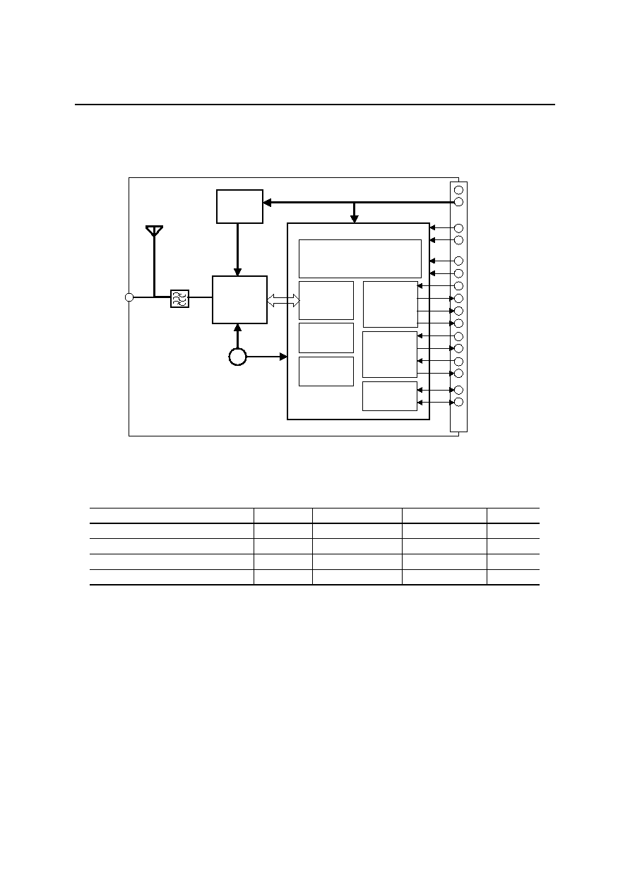
BLOCK DIAGRAM
RF_LSI
ML7050LA
ANT Chip
MK70120
PCM_IN
PCM_OUT
PCM_CLK
~
BPF
Osc.
13 MHz
PCM_SYNC
BB_LSI ML70Q511LA
4 Mbit
Flash ROM
CPU
ARM7TDMI
Baseband
Core
Voltage
Regulator
V
DD
GND
UART_RD
UART_TD
* UART_CTS
* UART_RTS
PCM
I/F
PCM
I/F
USB
I/F
USB_D+
USB_D≠
RESET
** XCLK
(32 kHz ±200 ppm)
VBUS
TEST1
Note: * indicates that the pin will be supported later.
** XCLK is optional
ANT
Connector
MK70110
32 KB
SRAM
20-Pin Connector
ABSOLUTE MAXIMUM RATINGS
Parameter Symbol
Condition
Rating
Unit
Power supply voltage
V
DD
Ta = 25∞C
≠0.3 to 4.5
V
Input voltage
V
IN
Ta = 25∞C
≠0.3 to 4.5
V
Input RF power
--
Ta = 25∞C
20
dBm
Storage temperature
T
stg
--
≠20 to +70
∞C

PEDLMK70-02
OKI Semiconductor
MK70110/MK70120
3/16
RECOMMENDED OPERATING CONDITIONS
Parameter Symbol
Condition
Min.
Typ.
Max.
Unit
Power supply voltage
V
DD
--
3.2
--
3.45
V
"H" level input voltage
V
ih
--
2.2
--
3.6
V
"L" level input voltage
V
il
--
0 -- 0.8 V
Operating temperature
T
OP
-- 0
25
50
∞C
ELECTRICAL CHARACTERISTICS
Specifications in this section are fulfilled under the conditions that V
DD
= 3.3 V ±0.1 V, Ta = 0 to 50∞C. Values of
the RF characteristics represent those specified at the edge of the module for both the MK70110 and the MK70120.
General Specifications
Items Specification
Note
Conformance Specifications
Bluetooth Specification
Version 1.1
--
Power Class
Class 2
--
Frequency range
2,402 to 2,480 MHz
--
Number of channels
79ch
--
Channel separation
1 MHz
--
Modulation method
GFSK
--
RF input-output impedance
Nominal 50
2,402 to 2,480 MHz
Symbol Rate
1 Mbps
--

PEDLMK70-02
OKI Semiconductor
MK70110/MK70120
4/16
DC Characteristics
Output voltage (Applies to digital pins except USB ports)
Parameter Symbol
Min.
Typ.
Max.
Unit
"H" level output voltage
V
oh
2.4 -- -- V
"L" level output voltage
V
ol
-- -- 0.4 V
Output voltage (Applies to USB ports (USB_D+, USB_D≠))
Parameter Symbol
Min.
Typ.
Max.
Unit
"H" level output voltage
V
oh
2.8 -- 3.6 V
"L" level output voltage
V
ol
-- -- 0.3 V
Power consumption (UART interface, with 32 kHz XCLK)
Mode Typ.
Max.
Unit
Initialize (Stop mode)
10
--
mA
Idle (Cold standby)
6
--
mA
Hold mode (Slave)
40
--
mA
Sniff mode (Slave)
40
--
mA
ACL connection DH1
103
125
mA
SCO connection HV1
113
135
mA
RF Transmission Characteristics
Parameter Min.
Max.
Unit
Remarks
Output power
≠6
+4
dBm
Frequency deviation
≠50
+50
kHz
Frequency drift
DH1
DH3,
DH5
≠25
≠40
+25
+40
kHz
kHz
Frequency shift
f1
avg
: payload = 11110000
f2
max
: payload = 1010...
f2
avg
/
f1
avg
140
115
80
175
--
--
kHz
kHz
%
20 dB band width
--
1
MHz
In-band spurious emission
Freq. offset = ±2 MHz
Freq.
offset
±3 MHz
--
--
≠20
≠40
dBm
dBm
Measured by peak detection
Out-of-band spurious emission
30
MHz
f < 1GHz
1
GHz
f
12.75 GHz
1.8
GHz
f
1.9 GHz
5.15
GHz
f
5.30 GHz
--
--
--
--
≠36
≠30
≠47
≠47
dBm
dBm
dBm
dBm

PEDLMK70-02
OKI Semiconductor
MK70110/MK70120
5/16
Reception Characteristics
Parameter Min.
Max.
Unit
Remarks
Reception sensitivity
--
0.1
%
at ≠70 dBm input
C/I characteristics
Co-channel
Adjacent channel C/I = 1 MHz
Adjacent channel C/I = 2 MHz
Adjacent channel C/I
3 MHz
Image
frequency
*2
Image frequency ±1 MHz
*2
--
--
--
--
--
--
14
4
≠30
*1
≠40
*1
≠6
≠16
dB
dB
dB
dB
dB
dB
Specification at ordinary temperature
(Bluetooth Ver.1.1 Test Specification)
Out-of-band blocking
30
MHz
f < 2,000 MHz
2,000
MHz
f
2,399 MHz
2,498
MHz
f < 3,000 MHz
3,000
MHz
f
12.75 GHz
≠10
≠27
≠27
≠10
--
--
--
--
dBm
dBm
dBm
dBm
Specification at ordinary temperature
Intermodulation characteristic
≠25
--
dB
Specification at ordinary temperature
Maximum input level
--
0.1
%
Specification at ordinary temperature, at
≠20 dBm input
Limit of collateral radio waves
30
MHz
f < 1 GHz
1
GHz
f
12.75 GHz
--
--
≠57
≠47
dBm
dBm
Spurious emission during inquiry scan
operation
*1 Relaxed C/I specification
On five spurious response frequencies with a distance of
2 MHz from the wanted signal (except for
image frequency and image ±1 MHz), a relaxed interference requirement C/I = ≠17 dB is applied.
(According to Bluetooth Specification 1.1, Part A Radio Specification)
*2 Image Frequencies and adjacent interference to image
Image frequency = Co-channel ≠4 MHz
±1 MHz adjacent interference to image frequency = Co-channel ≠3 MHz, Co-channel ≠5 MHz