FEDL2110-01
OKI Semiconductor
ML2110
4/101
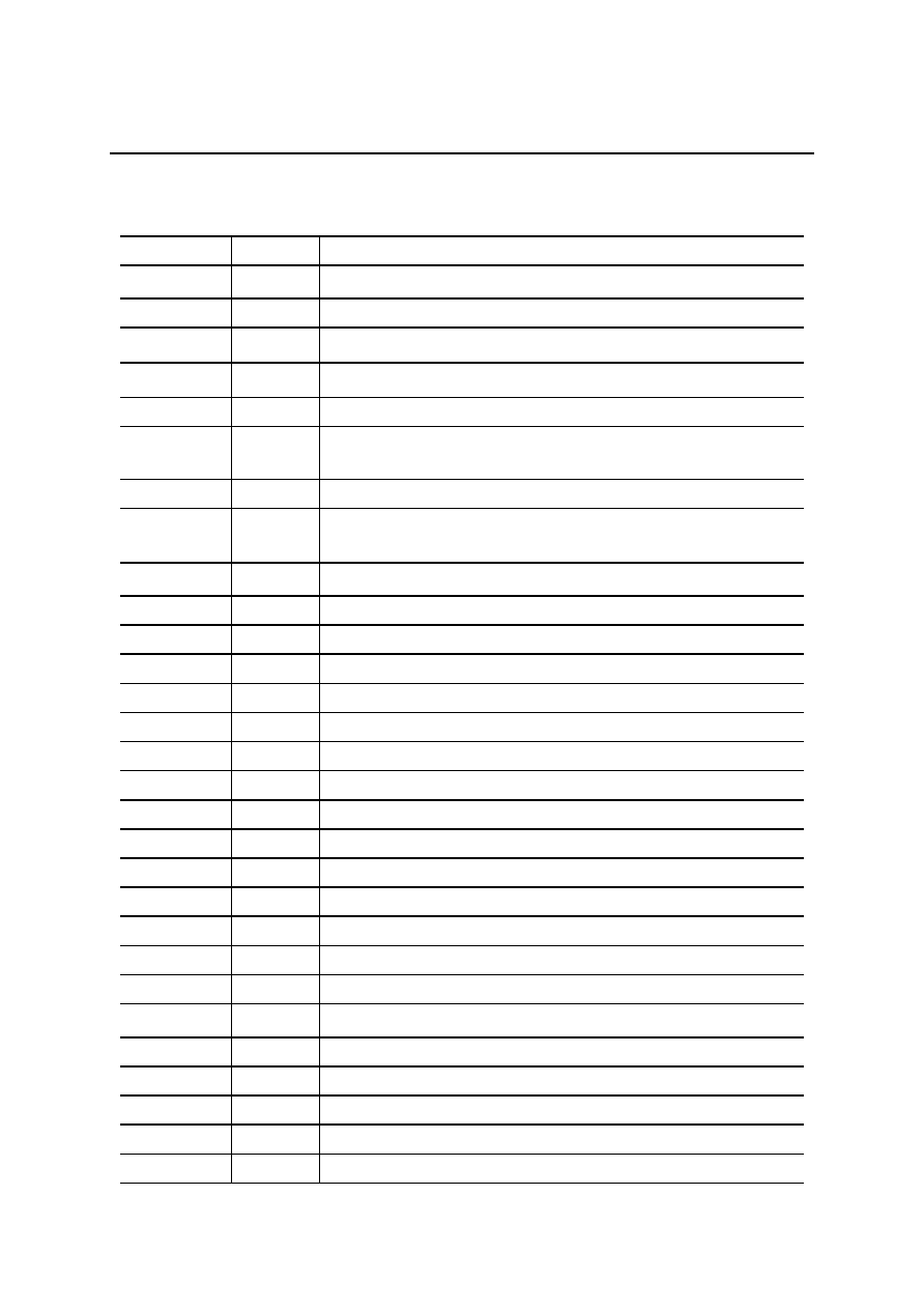
PIN DESCRIPTIONS
Symbol I/O
Description
D 31-0
I/O
32-bit data bus. 8-bit devices are accessed through D31-24. 16-bit devices
are accessed through D31-D16.
A23-0
O
24-bit address bus. DRAM addresses are output from A13-0.
ROM
O
ROM select signal.
ROM
indicates that ROM space is assigned to the
specified address. It is used as a chip select signal.
SRAM
O
SRAM select signal.
SRAM
indicates that SRAM space is assigned to the
specified address. It is used as a chip select signal.
RD
O
Read signal.
RD
is active during both 8-bit and 16-bit reads.
WR0-3
O
Write signals.
WR0
corresponds to writes from D31-24,
WR1
corresponds to
writes from D23-16,
WR2
corresponds to writes from D15-8, and
WR3
corresponds to writes from D7-0.
RAS
O
Row address strobe.
CAS0-3
O
Column address strobe.
CAS0
corresponds to accesses from D31-24,
CAS1
corresponds to accesses from D23-16,
CAS2
corresponds to accesses from
D15-8, and
CAS3
corresponds to accesses from D7-0.
WE
O
Write enable. WE is active during writes to DRAM space as the DRAM write
signal.
AS
O Address
strobe.
TXD
O
Serial data output.
RXD
I
Serial data input.
DTR
O
Control signal indicating SIO can transmit and receive.
DSR
I
Input signal indicating that modem is in operable state.
RTS
O
SIO transmit request signal.
CTS
I
Input signal indicating that modem can transmit.
SCLK
O
Synchronous transfer clock output.
PD7-0
I/O
Parallel port data input/output.
PACK
I
Parallel port read signal. Set high for Centronics interface.
PSTB
I
Parallel port write signal. Strobe signal for Centronics interface.
PCS
I
Parallel port chip select signal.
PIOA
I
Parallel port address signal. Selects data or status during an access.
POBF
3-state
Output port buffer full. Indicates that data has been set in the output buffer.
PIBF 3-state
Input port buffer full. Indicates that there is data in the input buffer.
Busy output signal for Centronics interface.
UPORT1-0
O
General flag output signal.
XSYNC
I
Synchronous transmit clock.
BCLK
I
Shift clock for DOUT.
DOUT
O
Digital signal output.
DAO
O
D/A Converter output.

FEDL2110-01
OKI Semiconductor
ML2110
5/101
Symbol I/O
Description
CLK
I
Clock input signal.
XO
O
Clock signal. Inverse of CLK.
CLKA
O
Internal clock signal.
CLKB
O
Internal clock signal. Inverse of CLK.
CLKENA
I
Clock change signal.
CLKFDBL
I
Clock cycle change signal.
RST
I Reset
input.
STBY
I
Standby signal.
STBY
suspends operation and places ML2110 in a standby
state.
EXTINT1-0
I
External interrupt signal.
WAIT
I/O
Wait signal. Normally, it is pulled up `H' level.
BR3
I
Cache/BIU test signal.
BGT3
O
Cache/BIU test signal.
MD
I
16/32 bit select signal.
TSTM2-0
I
Test mode select input signal.


