
FEDL2213-01
1Semiconductor
This version: May 2001
ML2213
Speech Synthesizer plus Music LSI with On-Chip 1.5 Mbit Mask ROM
1/26
GENERAL DESCRIPTION
The ML2213 is an ADPCM-based Speech Synthesizer LSI with on-chip 1.5 Mbit Mask ROM for storing multiple
speech data. In addition, the LSI has a built-in Music Generator circuit that can generate music by automatically
acquiring user-defined musical notes data from the ROM. The ML2213 contains a 12-bit D/A Converter and Low
Pass Filter, and enables a user to readily built a message and music playback sub-system by simply adding an
external speaker and driving amplifier.
FEATURES
∑
On-Chip 1.5 Mbit Mask ROM
∑
Serial Interface:
User-selectable Mask options for 2-pin or 3-pin interfacing
∑
3 Speech Synthesis Algorithms for user selection
4-bit ADPCM/8-bit OKI Non-Linear PCM/8-bit PCM/Music
∑
Sampling Frequency (At 4.096 MHz External Clock)
4.0 kHz, 5.3 kHz, 6.4 kHz, 8.0 kHz, 10.7 kHz, 12.8 kHz, 16.0 kHz
∑
Built-in Music Generator function
User-definable 31 musical scales, 60 musical notes, and 30 tempos
∑
User-defined Phrases up to 247 phrases, including music.
∑
Built-in 12-bit D/A Converter
∑
Built-in Low Pass Filter
∑
Driver for piezo-speaker (MD pin)
∑
External Clock:
Frequency can be selected as Mask option
4.096 MHz, 8.192 MHz, 16.384 MHz
∑
Power Supply Voltage:
2.4 to 5.5 V
∑
Package:
24-pin plastic SOP (SOP24-P-430-1.27-K) (Product name: ML2213-xxxMA)
14-pin plastic SSOP (SSOP14-P-44-0.65-K) (Product name: ML2213-xxxMB)

FEDL 2213-01
1Semiconductor
ML2213
2/26
BLOCK DIAGRAM
Frase Address
Latch
1.5 Mbit
ROM
ADPCM
Synthesizer
PCM
Synthesizer
12 bit DAC
LPF
18 bit
Multiplexer
18 bit
Address Counter
I/O
Interface
Timing Controller
AOUT
MD
RESET
GND
V
DD
CLK
NAR
BUSY
SI
SD
ST
MELODY
Address
Controller

FEDL 2213-01
1Semiconductor
ML2213
3/26
PIN CONFIGURATION (TOP VIEW)
NC: No connection
Note : If the 14-Pin Plastic SSOP is used, contact the Oki sales office for availability and specifications.
1
2
3
4
5
6
7
NC
NAR
BUSY
MD
GND
AOUT
NC
NC
SD
SI
RESET
CS
CLK
V
DD
14
13
12
11
10
9
8
6
7
1
2
3
4
5
NC
24
23
22
21
20
8
9
10
11
12
NC
NC
NC
AOUT
GND
MD
NAR
BUSY
NC
NC
NC
NC
NC
V
DD
CLK
ST
NC
RESET
SI
SD
NC
NC
NC
13
14
15
16
17
18
19
14-Pin Plastic SSOP
24-Pin Plastic SOP

FEDL 2213-01
1Semiconductor
ML2213
4/26
PIN DESCRIPTIONS
Pin
Symbol
Type
Description
11 (19)
RESET
l
"L" input to this pin turns the LSI into standby mode. At this point, output from
the AOUT pin rises up to V
DD
level, having the LSl initialized internally. By "H"
input to the pin the AOUT output returns to 1/2 V
DD
level.
2 (4)
NAR
O
This pin outputs a signal showing empty/full status of the Phase Address
Latch Resister. "H" level indicates the register is empty, and thus the LSI is
ready to accept serial data input. At powering up, the pin outputs "H level".
3 (5)
BUSY
O
Output "L" level while output signal is present either at the AOUT or MD pin.
At powering up, the pin outputs "H" level.
4 (6)
MD
O
Music output pin
6 (9)
AOUT
O
Analog output pin
5 (8)
GND
--
Ground pin
9 (16)
CLK
l
External clock input pin
12 (20)
Sl
l
Serial clock input pin
13 (21)
SD
l
Serial data input pin. Input a phrase code corresponding to a phrase address
through this pin.
10 (17)
ST
l
Chip select signal pin. Mask option allows a user to choose either 2-pin (SD
and Sl) interfacing or 3-pin (SD, Sl and
ST
) interfacing. When 3-pin inter-
facing is selected, input to the SD and Sl pins is valid while the
ST
pin being
held "L". When 2-pin interfacing is selected, pull this pin down to the GND.
8 (15)
V
DD
--
Power supply pin. Insert 0.1
µ
F or larger bypass capacitor between this pin
and the GND pin.
* 14-pin plastic SSOP (24-pin plastic SOP)

FEDL 2213-01
1Semiconductor
ML2213
5/26
ABSOLUTE MAXIMUM RATINGS
Parameter
Symbol
Condition
Rating
Unit
Power Supply Voltage
V
DD
≠0.3 to +7.0
V
Input Voltage
V
IN
Ta = 25∞C
≠0.3 to V
DD
+0.3
V
Storage Temperature
T
STG
--
≠55 to +150
∞C
RECOMMENDED OPERATING CONDITIONS
Parameter
Symbol
Condition
Range
Unit
Power Supply Voltage
V
DD
--
2.4 to 5.5
V
Operating Temperature
T
OP
--
≠40 to +85
∞C
4.096
8.192
External Clock Frequency
f
EXTCK
Selected as Mask options
16.384
MHz
ELECTRICAL CHARACTERISTICS
DC Characteristics (3 V Version)
(V
DD
= 2.4 to 3.6 V, GND = 0 V, Ta = ≠40 to +85∞C)
Parameter
Symbol
Condition
Min.
Typ.
Max.
Unit
"H" Input Voltage
V
IH
--
0.87
◊
V
DD
--
--
V
"L" Input Voltage
V
IL
--
--
--
0.13
◊
V
DD
V
"H" Output Voltage
V
OH
l
OH
= ≠500
µ
A
V
DD
≠0.3
--
--
V
"L" Output Voltage
V
OL
l
OL
= 1 mA
--
--
0.4
V
"H" Input Current
I
IH
V
IH
= V
DD
--
--
10
µ
A
"L" Input Current
I
IL
V
IL
= GND
≠10
--
--
µ
A
Operating Power Consumption
I
DD
--
--
1
4
mA
Standby Power Consumption
I
DS
Ta = ≠40 to +85∞C
--
--
10
µ
A
DA Output Relative Error
|V
DAE
|
--
--
--
40
mV
DC Characteristics (5 V Version)
(V
DD
= 3.7 to 5.5 V, GND = 0 V, Ta = ≠40 to +85∞C)
Parameter
Symbol
Condition
Min.
Typ.
Max.
Unit
"H" Input Voltage
V
IH
--
0.85
◊
V
DD
--
--
V
"L" Input Voltage
V
IL
--
--
--
0.15
◊
V
DD
V
"H" Output Voltage
V
OH
l
OH
= ≠500
µ
A
V
DD
≠0.3
--
--
V
"L" Output Voltage
V
OL
l
OL
= 1 mA
--
--
0.4
V
"H" Input Current
I
IH
V
IH
= V
DD
--
--
10
µ
A
"L" Input Current
I
IL
V
IL
= GND
≠10
--
--
µ
A
Operating Power Consumption
I
DD
--
--
2
4
mA
Standby Power Consumption
I
DS
Ta = ≠40 to +85∞C
--
--
10
µ
A
DA Output Relative Error
|V
DAE
|
--
--
--
40
mV

FEDL 2213-01
1Semiconductor
ML2213
6/26
AC Characteristics
(V
DD
= 2.4 to 5.5 V, GND = 0 V, Ta = ≠40 to +85∞C)
Parameter
Symbol
Condition
Min.
Typ.
Max.
Unit
CLK Duty Cycle
f
duty
--
40
50
60
%
RESET
Input Pulse Width
t
W(
RST
)
--
10
--
--
µ
s
RESET
Input Time after
Powering Up
t
D(
RST
)
--
0
--
--
µ
s
Serial Clock Pulse Width
t
W(Sl)
--
350
--
--
ns
Start Pulse Width
t
SDST
With 2-pin interfacing
1
--
--
µ
s
Serial Data Setup Time
t
SDS
--
1
--
--
µ
s
Serial Data Hold Time
t
SSD
--
1
--
--
µ
s
Serial Clock Setup Time
t
SlS
With 3-pin interfacing
1
--
--
µ
s
Serial Clock Hold Time
t
SSI
With 3-pin interfacing
1
--
--
µ
s
Analog Characteristics
(V
DD
= 2.4 to 5.5 V, GND = 0 V, Ta = ≠40 to +85∞C)
Parameter
Symbol
Condition
Min.
Typ.
Max.
Unit
AOUT Output Voltage Range
V
AO
--
V
DD
/4
--
V
DD
V
AOUT Pull-up Resistor Value
R
AO
--
2.5
--
5.0
k

FEDL 2213-01
1Semiconductor
ML2213
7/26
AOUT Equivalent Circuit
As shown above, the ML2213 uses current type DACs.
AOUT
RAO
Internal reference voltage
Internal control signal

FEDL 2213-01
1Semiconductor
ML2213
8/26
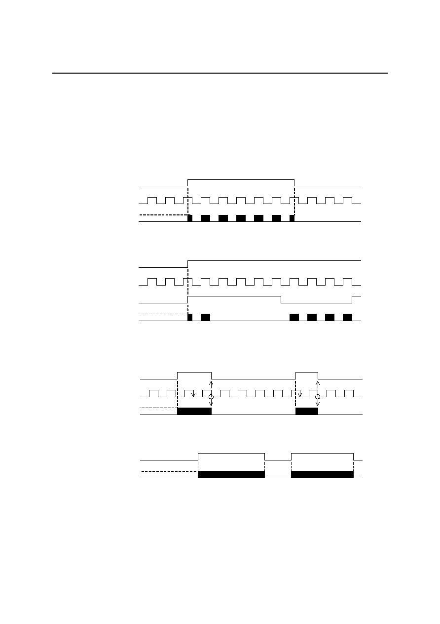
TIMING DIAGRAM
1. At powering up
2. Activating the LSI and Standby status
2.1 When 2-pin interfacing selected as Mask option
2.2 When 3-pin interfacing selected as Mask option
RESET
SD
SI
t
SDST
t
SDS
t
SSD
t
W(SI)
NAR
BUSY
AOUT
V
DD
RESET
BUSY
t
D(
RST
)
t
w(
RST
)
RESET
SD
SI
t
SIS
NAR
BUSY
AOUT
STC
t
SSI

FEDL 2213-01
1Semiconductor
ML2213
9/26
3
.
Co
nt
inuo
us P
l
a
y
b
a
c
k
Ti
m
i
ng
3.1 W
h
en
2-p
i
n
i
n
terfaci
n
g s
e
l
ected
as
Mas
k
op
ti
on
P
h
r
a
se
1 a
ddr
e
ss
sett
ing
Phrase
1 p
l
ay
ba
ck
P
h
r
a
se
2 a
ddr
e
ss
sett
ing
Phrase
2 p
l
ay
ba
ck
P
h
r
a
se
3 a
ddr
e
ss
sett
ing
Phrase
3 p
l
ay
ba
ck
ST
OP c
o
rd in
p
ut
RESE
T
SI
SD
NAR
BUSY
AOUT
RESE
T
SI
SD
NAR
BUSY
AOUT
2
)
Continuous
pla
y
ba
c
k
by
BU
S
Y
1
)
Continuous
pla
y
ba
c
k
by
N
A
R
ST
OP c
o
rd in
p
ut
P
h
r
a
se
3 a
ddr
e
ss
sett
ing
P
h
r
a
se
2 a
ddr
e
ss
sett
ing
P
h
r
a
se
1 a
ddr
e
ss
sett
ing
Phrase
3 p
l
ay
ba
ck
Phrase
2 p
l
ay
ba
ck
Phrase
1 p
l
ay
ba
ck

FEDL 2213-01
1Semiconductor
ML2213
10/26
3.2 W
h
en
3-p
i
n
i
n
terfaci
n
g s
e
l
ected
as
Mas
k
op
ti
on
RESE
T
ST
SI
SD
NAR
BUSY
AOUT
RESE
T
ST
SI
SD
NAR
BUSY
AOUT
2
)
Continuous
pla
y
ba
c
k
by
BUSY
1
)
Continuous
pla
y
ba
c
k
by
N
A
R
Phrase
1 a
ddre
ss
sett
ing
P
hrase
2 a
ddre
ss
sett
ing
P
hrase
3 a
ddre
ss
sett
ing
ST
OP c
o
rd in
p
ut
Phrase
1 p
l
ay
ba
ck
Phrase
2 p
l
ay
ba
ck
Phrase
3 p
l
ay
ba
ck
ST
OP c
o
rd in
p
ut
Phrase
3 p
l
ay
ba
ck
P
h
r
a
se
3 a
ddr
e
ss
sett
ing
P
h
r
a
se
2 a
ddr
e
ss
sett
ing
Phrase
2 p
l
ay
ba
ck
Phrase
1 p
l
ay
ba
ck
P
h
r
a
se
1 a
ddr
e
ss
sett
ing

FEDL 2213-01
1Semiconductor
ML2213
11/26
FUNCTIONAL DESCRIPTION
1. Specifying a user-defined phrase code for playback
The LSI allows a user to define up to 247 phrases. To playback a user-defined phrase, input a phrase code (phrase
address) in serial order, starting with the MSB, through the SD pin.
Figure 1.1 Timing for Phrase Code Input
When more than 8 SI clocks are input, the first 8-clock data is taken as valid data. Table 1.1 shows phrase codes
for user-defined phrases.
Table 1.1 Phrase Code for User-defined Phrase
MSB to LSB
Code Description
00000000
Stop Code
00000001
∑
∑
11110111
User-defined Phrase Codes
11111000
∑
∑
11111111
Test Codes*
Note: * No test codes could be used to represent a user-defined phrase.
2. Use-Prohibited Area in on-chip Mask ROM
As shown in the Table 2.1, the last 3 bytes of on-chip Mask ROM are use-prohibited. Be sure not to use the last 3
bytes when you prepare ROM data using an analyzing tool.
Table 2.1 shows addresses that are prohibited to use, and Figure 2.1 shows the address map of on-chip Mask ROM.
Table 2.1 User's Data Area and Use-Prohibited Area in on-chip Mask ROM
User's Data Area
Use-Prohibited Area
007C8 to 2FFFC
2FFFD, 2FFFE, 2FFFF
SD
SI
MSB 2SB 3SB 4SB 5SB 6SB 7SB LSB

FEDL 2213-01
1Semiconductor
ML2213
12/26
00000H
007C7H
Phrase Control Table Area
007C8H
2FFFCH
User's Date Area
2FFFDH
2FFFFH
Test Date Area
Figure 2.1 Mask ROM Address Map
3. Mask Options
The following mask options are available to choose an interfacing type and an external clock frequency, as shown
in Table 3.1.
Table 3.1 Mask Options
Option
Interfacing Type
External Clock Frequency
A
3-pin Interfacing
4.096 MHz
B
3-pin Interfacing
8.192 MHz
C
3-pin Interfacing
16.384 MHz
D
2-pin Interfacing
4.096 MHz
E
2-pin Interfacing
8.192 MHz
F
2-pin Interfacing
16.384 MHz
4. Interfacing Types
Mask option allows a user to select a interfacing type and a frequency of external clock input. Available options
are listed in Table 3.1 below.
4.1 2-pin Controlled Serial Input Interface
2-pin interfacing uses the SD and SI pins to control interfacing. Pull the
ST pin down to "L".
Figure 4.1 Timing Chart of Serial Input
As shown in Figure 4.1, serial data input is enabled by entering 1
µ
sec or longer "L" input (the Start-bit input) to
the SD pin. Serial data input to the SD pin is fetched to the internal register in synchronization with the falling
edge of the SI's 8th clock as a phrase code for a user-defined phrase.
SD
SI
NAR
BUSY
t
SDST

FEDL 2213-01
1Semiconductor
ML2213
13/26
You must input the external clock to the CLK pin. Otherwise, serial data input cannot be acquired internally,
regardless t
SDST
1
µ
s or t
SDST
< 1
µ
s.
Figure 4.2 Timing Chart of Serial Input
As shown in Figure 4.2, re-inputting the Start-bit before the SI's 8th clock cancels the preceding serial data entry,
and 8-clock data following the Start-bit is taken as valid data.
4.2 3-pin Controlled Serial Input Interface
3-pin interfacing uses the SD, SI and
ST pins to control interfacing.
Figure 4.3 Timing Chart of Serial Input
When 3-pin interfacing is selected, input to the SD and SI pins is enabled while the
ST pin being held "L". Serial
data input to the SD pin is acquired to the internal register in synchronization with the falling edge of the SI's 8th
clock as an 8-bit phrase code for a user-defined phrase. If the
ST pin is brought back to "H" before the SI's 8th
clock, the preceding entry is cancelled, and 8-clock data after the
ST pin being brought back to "L" again is taken
as valid data.
SD
SI
NAR
BUSY
t
SDST
t
SDST
SD
SI
NAR
BUSY
ST

FEDL 2213-01
1Semiconductor
ML2213
14/26
5. External Clock Input
Mask option allows a user to choose an external clock frequency, as shown in Table 5.1.
Table 5.1 External Clock Frequency and Sampling Frequency
External Clock Frequency
Internal Sampling Frequency
4.096 MHz
4.0 kHz, 5.3 kHz, 6.4 kHz, 8.0 kHz, 10.7 kHz, 12.8 kHz, 16.0 kHz
8.192 MHz
4.0 kHz, 5.3 kHz, 6.4 kHz, 8.0 kHz, 10.7 kHz, 12.8 kHz, 16.0 kHz
16.384 MHz
4.0 kHz, 5.3 kHz, 6.4 kHz, 8.0 kHz, 10.7 kHz, 12.8 kHz, 16.0 kHz
When an external clock frequency were chosen as Mask option and a different frequency input were made, the
sampling frequency changes in proportion to the actual input frequency. For example, while 4.096 MHz external
clock frequency option was selected as Mask option, and when 6.144 MHz external clock is actually input, then
the sampling frequency changes accordingly, e.g. sampling frequency at 1.5 times of those shown in Table 5.1.
6. Stop Code
The Stop code input (Table 1.1) to the SD pin during playback let the LSI stop playback on the SI's falling edge
following to the LSB input, and the AOUT fall down to 1/2 V
DD
level. If the LSI playbacks a music phrase, music
stops as well.
Timings for the Stop code input are shown below, for 2-pin interfacing in Figure 6.1 and for 3-pin interfacing in
Figure 6.2 respectively.
Figure 6.1 Timing for Stop Code Input - 2-pin Interfacing
Figure 6.2 Timing for Stop Code Input - 3-pin Interfacing
SD
SI
BUSY
STOP
SD
SI
BUSY
STOP
ST

FEDL 2213-01
1Semiconductor
ML2213
15/26
7. Music Generator
The Music Generator circuit initiates music output via the MD pin by activating a user-defined music phrase from
an external controller. The Music Generator outputs music, automatically acquiring musical notes data stored in
the Mask ROM. Acquiring the last note code where the end-bit is set to "1", results in stopping playback.
A user can define a music phrase by entering the starting address and tempo data in the Phrase Control Table, and
codes for musical notes and the end-bit information in the User's Data area. These data for a music phrase, based
on the score of music, can be created and entered by using an OKI's Analyzing Tool according to coding rules and
formats described later in this document.
7.1 Tempo Data
Tempo data for a music phrase can be defined in the Phrase Control Table while preparing ROM data. Tempo
cannot be changed from an external controller.
Tempo data defines a beat and rhythm for a music phrase. Table 7.1 lists tempos (the count of quarter notes per
minute) available for user's selection.

FEDL 2213-01
1Semiconductor
ML2213
16/26
Table 7.1 Tempos for Music Phrases
TEMPO
TP4
TP3
TP2
TP1
TP0
Tempo
0H
0
0
0
0
0
= 625
1H
0
0
0
0
1
= 625
2H
0
0
0
1
0
= 416.7
3H
0
0
0
1
1
= 312.5
4H
0
0
1
0
0
= 250
5H
0
0
1
0
1
= 208.3
6H
0
0
1
1
0
= 178.6
7H
0
0
1
1
1
= 156.7
8H
0
1
0
0
0
= 138.9
9H
0
1
0
0
1
= 125
AH
0
1
0
1
0
= 113.6
BH
0
1
0
1
1
= 104.2
CH
0
1
1
0
0
= 96.2
DH
0
1
1
0
1
= 89.3
EH
0
1
1
1
0
= 83.3
FH
0
1
1
1
1
= 78.1
10H
1
0
0
0
0
= 73.5
11H
1
0
0
0
1
= 69.4
12H
1
0
0
1
0
= 65.8
13H
1
0
0
1
1
= 62.5
14H
1
0
1
0
0
= 59.5
15H
1
0
1
0
1
= 56.8
16H
1
0
1
1
0
= 54.3
17H
1
0
1
1
1
= 52.1
18H
1
1
0
0
0
= 50
19H
1
1
0
0
1
= 48.1
1AH
1
1
0
1
0
= 46.3
1BH
1
1
0
1
1
= 44.6
1CH
1
1
1
0
0
= 43.1
1DH
1
1
1
0
1
= 41.7
1EH
1
1
1
1
0
= 40.3
1FH
1
1
1
1
1
= 39.1

FEDL 2213-01
1Semiconductor
ML2213
17/26
7.2 Musical Note Data
Musical note data consists of 2 bytes and is stored in the Mask ROM's User's Data area, where a user can define
scale, note and the end-bit for a music phrase. Table 7.2 shows the coding format for musical note data.
Table 7.2 Coding Format for Musical Note Data
NSB
7SB
6SB
5SB
4SB
3SB
2SB
LSB
The First Byte END-Bit
0
L5
L4
L3
L2
L1
L0
Musical Note Code
The Second Byte
N7
N6
N5
N4
N3
N2
N1
N0
Musical Scale Code
(1) Musical Scale Code
Musical scale code is defined at the second byte. The following equation shows output frequency from the Music
Generator circuit at 4.096 MHz external clock.
kHz ("N" is integer between 4 to 127)
Co-relationship between "N" and musical scale can be calculated as follows:
N = 2
7
N7 + 2
6
N6 +2
5
N5 + 2
4
N4 + 2
3
N3 + 2
2
N2 + 2
1
N1 + 2
0
N0
When all values for N7 to N2 are set to "0", no music is reproduced during the period specified by the note code.
At this instance, the values of N1 and N0 have no significance (Don't care).
Table 7.3 shows major musical scales (keys) and their corresponding scale codes.
32
(N + 2)
FEDL 2213-01
1Semiconductor
ML2213
18/26
Table 7.3 Musical Scales and Corresponding Scale Codes
Scale Code
Musical
Scale
Frequency
(Hz)
N7
N6
N5
N4
N3
N2
N1
N0
N7 to N0
C
1
261.22
1
1
1
1
0
0
1
1
F3H
Cis
1
277.06
1
1
1
0
0
1
0
1
E5H
D
1
293.58
1
1
0
1
1
0
0
0
D8H
Dis
1
310.68
1
1
0
0
1
1
0
0
CCH
E
1
329.90
1
1
0
0
0
0
0
0
C0H
F
1
349.73
1
0
1
1
0
1
0
1
B5H
Fis
1
369.94
1
0
1
0
1
0
1
1
ABH
G
1
392.64
1
0
1
0
0
0
0
1
A1H
Gis
1
415.58
1
0
0
1
1
0
0
0
98H
A
1
441.38
1
0
0
0
1
1
1
1
8FH
Ais
1
467.15
1
0
0
0
0
1
1
1
87H
B
1
492.31
1
0
0
0
0
0
0
0
80H
C
2
524.59
0
1
1
1
1
0
0
0
78H
Cis
2
556.52
0
1
1
1
0
0
0
1
71H
D
2
587.16
0
1
1
0
1
0
1
1
6BH
Dis
2
621.36
0
1
1
0
0
1
0
1
65H
E
2
659.79
0
1
0
1
1
1
1
1
5FH
F
2
695.65
0
1
0
1
1
0
1
0
5AH
Fis
2
744.19
0
1
0
1
0
1
0
0
54H
G
2
780.49
0
1
0
1
0
0
0
0
50H
Gis
2
831.17
0
1
0
0
1
0
1
1
4BH
A
2
876.71
0
1
0
0
0
1
1
1
47H
Ais
2
927.54
0
1
0
0
0
0
1
1
43H
B
2
984.62
0
0
1
1
1
1
1
1
3FH
C
3
1049.18
0
0
1
1
1
0
1
1
3BH
Cis
3
1103.45
0
0
1
1
1
0
0
0
38H
D
3
1185.19
0
0
1
1
0
1
0
0
34H
Dis
3
1254.90
0
0
1
1
0
0
0
1
31H
E
3
1306.12
0
0
1
0
1
1
1
1
2FH
F
3
1391.30
0
0
1
0
1
1
0
0
2CH
Fis
3
1488.37
0
0
1
0
1
0
0
1
29H
(2) Musical Note Code
The first byte of music data code is where a user can define musical note code. Table 7.4 shows musical notes and
their corresponding note codes (L5 to L0). When all bits are set to "0", the duration or beat of the note is identical
to that of the code with L0 alone set to "1" (1/64).

FEDL 2213-01
1Semiconductor
ML2213
19/26
Table 7.4 Musical Notes and Corresponding Note Codes
Note Code
Musical Note
L5
L4
L3
L2
L1
L0
L5 to L0
1
1
1
1
1
1
3FH
1
0
1
1
1
1
2FH
0
1
1
1
1
1
1FH
0
1
0
1
1
1
17H
0
0
1
1
1
1
0FH
0
0
1
0
1
1
0BH
0
0
0
1
1
1
07H
0
0
0
1
0
1
05H
When N6 to N0 are set to "0" in scale code definition, the code means "Rest". Table 7.5 shows rests and their
corresponding rest codes (L5 to L0).
Table 7.5 Rests and Corresponding Rest Codes
Rest Code
Rest
L5
L4
L3
L2
L1
L0
L5 to L0
1
1
1
1
1
1
3FH
0
1
1
1
1
1
1FH
0
1
0
1
1
1
17H
0
0
1
1
1
1
0FH
0
0
0
1
1
1
07H
0
0
0
0
1
1
03H
The following formula can be used to calculate the duration or beat of a musical note (including rest), that is
defined by a note code and tempo code.
1.5
◊
(TP+1)
◊
(L+1) msec (Where TP is integer between 1 to 31, and L is integer between 4 to 63)
TP is a numerical value defined in the Phrase Control Table and its bit correspondence to tempo data can be
calculated as follows:
TP = 2
4
TP4 + 2
3
TP3 + 2
2
TP2 + 2
1
TP1 + 2
0
TP0
Meanwhile, L is defined by a musical note code, and its bit correspondence to the musical note code can be
calculated as follows:
L = 2
5
L5 + 2
4
L4 + 2
3
L3 + 2
2
L2 + 2
1
L1 + 2
0
L0

FEDL 2213-01
1Semiconductor
ML2213
20/26
(3) End-Bit
The end-bit is set at the first byte, the MSB, of music phrase data. As soon as the LSI starts to output the last note
code where the end-bit is set to "1", the Music Generator circuit issues an end-music interrupt call and stops
playback after the last note code has been output.
7.3 Sample Musical Note Codes
Table 7.6 shows sample codes to output a part of musical score shown in Figure 7.3.
Figure 7.3
Table 7.6 Coding Sample
Note Code
1st Byte
2nd Byte
7
6
5
4
3
2
1
0
7
6
5
4
3
2
1
0
Musical
Note
END --* L5
L4
L3
L2
L1
L0
N7
N6
N5
N4
N3
N2
N1
N0
Hexa-
decimal
G
2
0
0
1
0
1
1
1
1
0
1
0
1
0
0
0
0
2F50H
D
2
0
0
0
0
1
1
1
1
0
1
1
0
1
0
1
1
0F6BH
G
2
0
0
0
1
0
1
1
1
0
1
0
1
0
0
0
0
1750H
D
2
0
0
0
0
0
1
1
1
0
1
1
0
1
0
1
1
076BH
G
2
0
0
0
1
0
1
1
1
0
1
0
1
0
0
0
0
1750H
A
2
0
0
0
0
0
1
1
1
0
1
0
0
0
1
1
1
0747H
B
2
0
0
1
1
1
1
1
1
0
0
1
1
1
1
1
1
3F3FH
G
2
1
0
1
1
1
1
1
1
0
1
0
1
0
0
0
0
BF50H
Note: * Bit 6 of the first byte can be either "0" or "1" (Don't care bit), so is set to "0" in the above sample
codes.
=120
FEDL 2213-01
1Semiconductor
ML2213
21/26
8. Buzzer
You can define a buzz phrase by setting a frequency and sound type in the Phrase Control Table and a buzz phrase
in the User's Data area. To start buzzer output via the MD pin, activate a buzz phrase. To stop buzzer output, enter
the Stop Code.
4 buzzing sound types, intermittent 1, intermittent 2, single and continuous, and 3 50%-duty frequencies, at 0.5
kHz, 1.0 kHz and 2.0 kHz, are available for user selection, depending on buzzer output mode setup in the Phrase
Control Table.
Figure 8.1 shows output wave-form in respective output modes. Black-filled wave-form indicates buzz output
signal at 2 kHz.
(a) TP1 = 0, TP0 = 0 (intermittent 1)
(b) TP1 = 0, TP0 = 1 (intermittent 2)
(c) TP1 = 1, TP0 = 0 (single)
(d) TP1 = 1, TP0 = 1 (continuous)
Figure 8.1 Output Wave-form from the Buzzer Driver in Each Output Mode
ON
EMBD
8 Hz
OUTPUT MD
OFF
EMBD
8 Hz
OUTPUT MD
1 Hz
ON
OFF
EMBD
OUTPUT MD
ON
OFF
OUTPUT MD
EMBD
32 Hz
ON
OFF

FEDL 2213-01
1Semiconductor
ML2213
22/26
9. Low Pass Filter
ML2213's analog output goes through the built-in Low Pass Filter. The Figure 9.1 below shows Frequency
Characteristics and Table 9.1 shows Cut-off Frequency of the LPF.
No analog output passing through the LPF is available on this chip.
Figure 9.1 LPF Frequency Characteristics (f
SAM
= 8 kHz)
Table 9.1 LPF Cut-off Frequency
Sampling Frequency (kHz)
(f
SAM
)
Cut-off Frequency (kHz)
(f
CUT
)
4.0
1.2
5.3
1.6
6.4
2.0
8.0
2.5
10.6
3.2
12.8
4.0
16.0
5.0
10. AOUT Connecting Circuit
It is recommended to connect a capacitor of 0.01 to 0.033
µ
F to the AOUT pin.
The circuit diaram is as shown below.
The capacitor is used for improving a voice quality. Check the voice quality before determining the capacitor
value. If the voice quality is excellent without connecting a capacitor, no capacitor is required.
[dB] 20
10
0
≠10
≠20
≠30
≠40
≠50
≠60
≠70
≠80
10 100 1 k 10 k [Hz]
AOUT
0.01 to 0.033
µ
F

FEDL 2213-01
1Semiconductor
ML2213
23/26
APPLICATION CIRCUITS
When 2-pin interfacing is selected
(Fix the ST pin to GND.)
ML2213
AOUT
GND
V
DD
SD
RESET
MCU
SI
CLK
BUSY
NAR
MD
Piezoelectric
speaker
ST
AMP
AMP

FEDL 2213-01
1Semiconductor
ML2213
24/26
PACKAGE DIMENSIONS
SOP24-P-430-1.27-K
Mirror finish
Package material
Epoxy resin
Lead frame material
42 alloy
Pin treatment
Solder plating (
5µm)
Package weight (g)
0.58 TYP.
5
Rev. No./Last Revised
5/Oct. 13, 1998
Notes for Mounting the Surface Mount Type Package
The surface mount type packages are very susceptible to heat in reflow mounting and humidity
absorbed in storage.
Therefore, before you perform reflow mounting, contact Oki's responsible sales person for the product
name, package name, pin number, package code and desired mounting conditions (reflow method,
temperature and times).
(Unit : mm)

FEDL 2213-01
1Semiconductor
ML2213
25/26
SSOP14-P-44-0.65-K
Mirror Finish
Package material
Epoxy resin
Lead frame material
42 alloy
Pin treatment
Solder plating (
5µm)
Package weight (g)
0.066 TYP.
5
Rev. No./Last Revised
1/Sept. 18, 1998
Notes for Mounting the Surface Mount Type Package
The surface mount type packages are very susceptible to heat in reflow mounting and humidity
absorbed in storage.
Therefore, before you perform reflow mounting, contact Oki's responsible sales person for the product
name, package name, pin number, package code and desired mounting conditions (reflow method,
temperature and times).
(Unit: mm)

FEDL 2213-01
1Semiconductor
ML2213
26/26
NOTICE
1.
The information contained herein can change without notice owing to product and/or technical improvements.
Before using the product, please make sure that the information being referred to is up-to-date.
2.
The outline of action and examples for application circuits described herein have been chosen as an
explanation for the standard action and performance of the product. When planning to use the product, please
ensure that the external conditions are reflected in the actual circuit, assembly, and program designs.
3.
When designing your product, please use our product below the specified maximum ratings and within the
specified operating ranges including, but not limited to, operating voltage, power dissipation, and operating
temperature.
4.
Oki assumes no responsibility or liability whatsoever for any failure or unusual or unexpected operation
resulting from misuse, neglect, improper installation, repair, alteration or accident, improper handling, or
unusual physical or electrical stress including, but not limited to, exposure to parameters beyond the specified
maximum ratings or operation outside the specified operating range.
5.
Neither indemnity against nor license of a third party's industrial and intellectual property right, etc. is
granted by us in connection with the use of the product and/or the information and drawings contained herein.
No responsibility is assumed by us for any infringement of a third party's right which may result from the use
thereof.
6.
The products listed in this document are intended for use in general electronics equipment for commercial
applications (e.g., office automation, communication equipment, measurement equipment, consumer
electronics, etc.). These products are not authorized for use in any system or application that requires special
or enhanced quality and reliability characteristics nor in any system or application where the failure of such
system or application may result in the loss or damage of property, or death or injury to humans.
Such applications include, but are not limited to, traffic and automotive equipment, safety devices, aerospace
equipment, nuclear power control, medical equipment, and life-support systems.
7.
Certain products in this document may need government approval before they can be exported to particular
countries. The purchaser assumes the responsibility of determining the legality of export of these products
and will take appropriate and necessary steps at their own expense for these.
8.
No part of the contents contained herein may be reprinted or reproduced without our prior permission.
Copyright 2001 Oki Electric Industry Co., Ltd.