 | –≠–ª–µ–∫—Ç—Ä–æ–Ω–Ω—ã–π –∫–æ–º–ø–æ–Ω–µ–Ω—Ç: ML2302 | –°–∫–∞—á–∞—Ç—å:  PDF PDF  ZIP ZIP |

OKI Semiconductor
FEDL2302DIGEST-05
Issue Date: Dec. 27, 2004
ML2302
Recording and Playback LSI with Built-in 2-Bit ADPCM2 Supported FIFO
1/24
GENERAL DESCRIPTION
The ML2302 is a recording and playback LSI with built-in FIFO memories for buffering. It employs the new 2-bit
ADPCM2 algorithm in addition to conventional 4-bit OKIADPCM and 4-bit OKIADPCM2 algorithms.
The ML2302 operates at 2.7 to 3.6 V and supports a variety of applications.
FEATURES
∑ Built-in two 1024-bit FIFOs
(buffering time of 32 ms when using 8 kHz sampling frequency and 4-bit ADPCM)
∑ Supports five compression algorithms for recording and playback:
2-bit OKIADPCM2; 4/5/6/7-bit OKIADPCM2; 4-bit OKIADPCM; 8/16-bit straight PCM; 8-bit OKI
Nonlinear PCM
∑ Source oscillation frequency 16.384 MHz
∑ Sampling
frequency
(fsam)
4.0 to 12.8 kHz (OKIADPCM2)
4.0 to 25.6 kHz (8-bit straight PCM)
∑ Supports 8-bit bus interface.
∑ Built-in voice level detection function (VAC)
∑ Built-in noise injection function
∑ Supports
external DAC interface.
∑ Built-in volume control circuit
(0 dB to ≠44 dB: ≠2 dB step, ≠44 dB to ≠80 dB: ≠4 dB step)
∑ Built-in 14-bit A/D converter and 14-bit D/A converter
∑ Built-in low pass filter (LPF)
(recording side: analog filter, playback side: digital filter)
∑ Built-in speaker amplifier (100 mW, 8)
∑ Power supply voltage : +2.7 to +3.6 V
∑ Package
: 64-pin plastic TQFP (TQFP64-P-1010-0.50-K) (ML2302TB)
: 71-pin W ≠ CSP

FEDL2302DIGEST-05
OKI Semiconductor
ML2302
2/24
BLOCK DIAGRAM
MO
U
T
LO
U
T
MIN
DREQL
DACK
L
IO
W
IO
R
XT
X
T
RE
S
E
T
TEST0
TEST2
TEST3
TEST4
TEST5
TEST6
TEST7
TEST8
TEST9
VCK
SIOCK
ADSD
DASD
AV
DD
AGND
DV
DD
DGND
FIFOST
LIN
ADC
LPF
DAC
LPF
Volume
Controller
Analyzer
Synthesizer
FIFO
S
er
i
a
l
P
ort
MCU
I/F
EMP
MID
FUL
CH
BUSY
CBUSY
CS
D/
C
WR
RD
D7 to 0
DMA
I/F
Timing
Controller
AOUT
SPIN
SPOUT
-
SPOUT
+
VR
SPV
DD
CB1
CB2
SG
VOXO
◊
1
SG
VR
VR
SG

FEDL2302DIGEST-05
OKI Semiconductor
ML2302
3/24
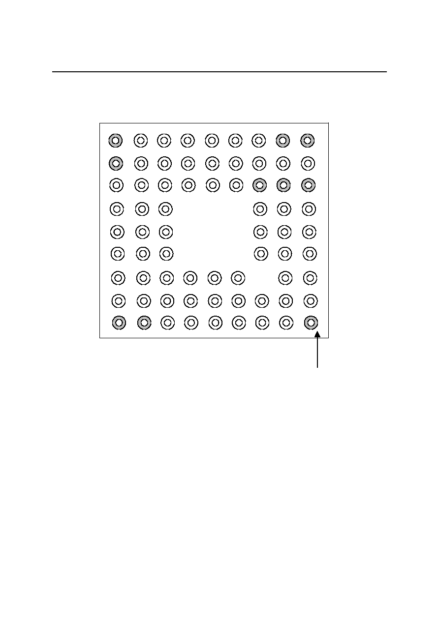
PIN CONFIGURATION (TOP VIEW)
N.C.: No Connection
64-pin plastic TQFP
C
S
D/
C
B
US
Y
SI
O
C
K
DASD
A
DSD
VC
K
DG
ND
D
AC
K
L
DR
EQ
L
I
OW
I
OR
VO
X
O
XT
X
T
TES
T
0
64
63
62
61
60
59
58
57
56
55
54
53
52
51
50
49
AV
DD
SG
LO
U
T
LI
N
MO
U
T
MI
N
AG
ND
TE
ST9
AO
U
T
SP
I
N
SPO
UT
≠
SP
O
U
T+
N.
C
.
N.
C
.
N.
C
.
AG
ND
(
S
P
)
17
18
19
20
21
22
23
24
25
26
27
28
29
30
31
32
D0
D1
D2
D3
D4
D5
D6
D7
DV
DD
TEST2
TEST3
TEST4
TEST5
TEST6
TEST7
TEST8
1
2
3
4
5
6
7
8
9
10
11
12
13
14
15
16
RD
WR
DV
DD
FUL
MID
EMP
CH
CBUSY
RESET
FIFOST
DGND
VR
CB1
CB2
SPV
DD
AV
DD
(SP)
48
47
46
45
44
43
42
41
40
39
38
37
36
35
34
33
FEDL2302DIGEST-05
OKI Semiconductor
ML2302
4/24
71-pin W-CSP (Bottom View)
G
F
E
D
C
B
A
1
2
3
4
5
6
7
FUL
N.C.
RD
CH
CB2
VR
RESET
INDEX
N.C.
N.C.
DV
DD
N.C.
TEST0
EMP
SPV
DD
CB1
FIFOST
AV
DD
(SP) AGND(SP)
WR
XT
XT
MID
N.C.
DGND
CBUSY
N.C.
N.C.
IOW
IOR
VOXO
SPOUT+ SPOUT≠ SPIN
DGND
DACKL
DREQL
AGND TEST9 AOUT
DASD
VCK
ADSD
LIN
MOUT
MIN
D/
C
SIOCK
BUSY
D4
TEST2
DV
DD
SG
LOUT
D1
CS
D0
D2
D6
TEST8
AV
DD
D3
N.C.
N.C.
D5
D7
N.C.
8
9
H
J
TEST3
TEST4
TEST5
TEST6 TEST7
FEDL2302DIGEST-05
OKI Semiconductor
ML2302
5/24
PIN DESCRIPTIONS
Pin
(WCSP)
Pin
(TQFP)
Symbol Type
Description
H2, G2,
F2, G1,
F3, F1,
E2, E1
1 to 8
D7 to 0
I/O
Bidirectional data bus.
Command and data inputs from an external microcontroller and
memory, and status and data outputs to an external
microcontroller and memory.
G7 47
WR
I
Write pulse input pin. This pin pulses "L" when command or
voice data is input to D7 to D0 pins.
H9 48
RD
I
Read pulse input pin. This pin pulses "L" when status or voice
data is output to D7 to D0.
J2 64
CS
I
Accepts write pulse and read pulse when this pin is "L".
G3 63 D/
C
I
Voice data is input or output to and from D7 to D0 when this pin
is "H".
H3 62
BUSY
O
This pin outputs a "L" level during RECORDING, PLAYBACK,
or PAUSE.
E7 41
CBUSY
O
Accepts a command during this pin is "H".
F8 43 EMP
O
"H" indicates that there is no data in FIFO memory.
During playback, voice synthesis starts when EMP changes to
"L". Active "H" can be changed to active "L".
F7 44 MID
O
"H" level indicates that there is more than half of the FIFO
memory.
G9 45 FUL
O
"H" level indicates that FIFO memory is full of data. During
playback, this pin is "H" and data cannot be written in FIFO
memory. During recording, data is not written after FIFO
memory is full of data.
Active "H" can be changed to active "L".
F9 42 CH
I
This pin should be set at a "L" level normally and be set at a "H"
level when DMA is used.
H5 55
DREQL
O
When DMA transfer is selected, "H" level DREQL outputs a
signal to request a DMA transfer. Active "H" can be changed to
active "L".
J5 56
DACKL
I
Input to
DACKL
a signal when DMA transfer is permitted by the
DMA controller. when DACKL is "L",
IOW
and
IOR
signals are
accepted.
Active "L" can be changed to active "H" by command input.
If DMA transfer is not used, set this pin to "H" level.
G6 54
IOW
I
Write pulse Input pin to write external memory data to ML2302
during DMA transfer. If DMA transfer is not used, set this pin to
"H" level.
J6 53
IOR
I
Read pulse input pin to read data of ML2302 during DMA
transfer.
If DMA transfer is not used, set this pin to "H" level.
H4 59
ADSD
I
16-bit serial data input pin when external A/D converter is used.
If external A/D converter is not used, set this pin to "L" level.
G4
60
DASD
O
16-bit serial data input pin when external D/A converter is used.
FEDL2302DIGEST-05
OKI Semiconductor
ML2302
6/24
Pin
(WCSP)
Pin
(TQFP)
Symbol Type
Description
J3 61
SIOCK
I/O
16-bit serial data transfer clock when external A/D or D/A
converter is used.
J4 58 VCK
I/O
Outputs sampling frequency selected. Input pin when slave
mode is selected.
J7
H7
51
50
XT
XT
I
O
Oscillator connection pins. when external clock is used, input
clock into XT pin and leave
XT
pin open. Oscillation stops
during reset or power down mode. Figure (a) shows Oscillation
Equivalent Circuit.
E9 40
RESET
I
When this pin is "L", the LSI is initialized and AOUT is set to the
GND level.
E8 39
FIFOST
I
When this pin is "L", EMP, MID, and FULL of playback FIFO can
be monitored. When this pin is "H", EMP, MID, and FULL of
record FIFO can be monitored.
B3 18 SG
O
Analog circuit signal ground pin. This pin is connected to GND
during reset or power down mode.
A4
C4
22
20
MIN
LIN
I
Inverting input pin for built-in OP amplifier. Non-inverting input
pin is connected to SG (Signal Ground).
B4
A3
21
19
MOUT
LOUT
O
MOUT is the output of internal OP amplifier to MIN, and LOUT
is to LIN.
A5
25
AOUT
O
This is the output of the analog playback waveform.
H6
52
VOXO
O
Voice level detection signal
H8, B2
49, 16
TEST0, 8
I
Pins for testing. Set the pins to "L".
E3, G8
9, 46
DV
DD
--
Digital power supply pin. Insert a minimum 0.1
µ
F bypass
capacitor between this pin and DGND pin
D7, G5
38, 57
DGND
--
Digital GND pin.
A2, B8
17, 33
AV
DD
--
Analog power supply pin. Insert a minimum 0.1
µ
F bypass
capacitor between this pin and AGND pin.
C5, A8
23, 32
AGND
--
Analog GND pin.
C9, D8
36
35
CB1
CB2
O
This pin is used to connect a capacitor for voltage multiplier
power supply. Insert a 1
µ
F capacitor between CB1 and CB2.
C8 34
SPV
DD
O
Voltage multiplier power supply output pin for speaker amplifier.
Connect a 1
µ
F capacitor to this pin in order to stabilize the
speaker amplifier circuit.
D9 37
VR
O
Bias output pin for speaker amplifier. Set this pin to the GND
level during reset or power down mode.
A6
26
SPIN
I
Voice signal input pin for speaker amplifier.
B6 27
SPOUT≠
O
Speaker amplifier output pin. This pin outputs a signal in
reverse phase to the signal that is input to the SPIN pin.
C6 28
SPOUT+
O
Speaker amplifier output pin. This pin outputs a signal in phase
to the signal that is input to the SPIN pin.
D1, D2,
D3, C1,
C2, B1,
B5
10~15
,24
TEST2 to
7, 9
O
Pins for testing. Leave these pins open.

FEDL2302DIGEST-05
OKI Semiconductor
ML2302
7/24
Figure (a) Oscillation Equivalent Circuit
RESET
power down
XT
XT
Internal OSC

FEDL2302DIGEST-05
OKI Semiconductor
ML2302
8/24
ABSOLUTE MAXIMUM RATINGS
Parameter Symbol
Condition
Rating
Unit
Power Supply Voltage
V
DD
≠0.3 to +7.0
V
Input Voltage
V
IN
≠0.3 to V
DD
+0.3
V
Maximum Power Dissipation
PD
Ta = 25∞C
689.6 mW
Temperature Storage
T
STG
--
≠55 to +150
∞C
RECOMMENDED OPERATING CONDITIONS
Parameter Symbol
Condition
Rating
Unit
Power Supply Voltage
V
DD
DGND = AGND = 0 V
+2.7 to +3.6
V
Operating Temperature
T
Op
--
≠10 to +70
∞C
Master Clock Frequency
f
OSC
-- 16.384
MHz
Speaker Amplifier Load Impedance
R
LSP
-- 8
to

FEDL2302DIGEST-05
OKI Semiconductor
ML2302
9/24
ELECTRICAL CHARACTERISTICS
DC Characteristics
(DV
DD
= AV
DD
= 2.7 to 3.6 V, DGND = AGND = 0 V, Ta = ≠10 to +70∞C)
Parameter Symbol
Condition Min.
Typ.
Max.
Unit
High-level Input
Voltage
V
IH
--
0.85
◊
V
DD
-- --
V
Low-level Input
Voltage
V
IL
-- --
--
0.15
◊
V
DD
V
High-level Output
Voltage
(*1, *5)
V
OH1
V
DD
≠ 0.3
--
--
V
High-level Output
Voltage
(*2, *5)
V
OH2
I
OH
= ≠40 µA
V
DD
≠ 0.3
--
--
V
Low-level Output
Voltage (*1,
*5)
V
OL1
--
--
0.45
V
Low-level Output
Voltage
(*2, *5)
V
OL2
I
OL
= 2 mA
-- -- 0.8
V
High-level Input
Current
(*3)
I
IH1
--
--
10
µA
High-level Input
Current
(*4)
I
IH2
V
IH
= V
DD
1 -- 7
µA
Low-level Input
Current
(*3)
I
IL1
≠10
--
--
µA
Low-level Input
Current
(*4)
I
IL2
V
IL
= GND
≠7 -- ≠1
µA
Operating Current
Consumption
I
DD
f
osc
= 16 MHz, without load
--
15
20
mA
At reset, without load
Ta = ≠10 to +50∞C
-- -- 10
µA
Standby Current
Consumption
I
DDS
At reset, without load
Ta = +50 to +70∞C
-- -- 50
µA
*1 : Applied to input pins excluding XT pin.
*2 : Applied to XT pin.
*3 : Applied to output pins excluding XT pin.
*4 : Applied to XT pin.
*5 : If an output pin is shortcircuited to V
DD
or GND, the LSI may be damaged.
FEDL2302DIGEST-05
OKI Semiconductor
ML2302
10/24
Analog Characteristics
(DV
DD
= AV
DD
= 2.7 to 3.6 V, DGND = AGND = 0 V, Ta = ≠10 to +70∞C)
Parameter Symbol
Condition Min.
Typ.
Max.
Unit
D/A Output Relative
Error
|V
DAE
| Without
load --
--
40
mV
LOUT Allowable Voltage
Range
V
LOUT
V
DD
= 3 V
0.75
--
2.25
V
OP Amplifier Open Loop
Gain
G
OP
f
in
= 0 to 4 kHz
40
--
--
dB
DAC Output Impedance
R
DAO
DAC output is selected
AOUT = 1/2V
DD
30 50 70
k
OP Amplifier Input
Impedance
R
INA
(Excluding MIC amplifier)
1
--
--
M
MIC Amplifier Input
Impedance
R
INAM
MIC
amplifier 8.1 11.6 15.1
k
MOUT, LOUT Load
Resistance
R
OUTA
-- 50
--
--
k
AOUT Load Resistance
R
AOL
-- 50
--
--
k
VR Output Voltage
V
VR
--
1.22 1.25 1.28 V
SG Output Voltage
V
SG
V
DD
= 3.0 V
1.47
1.5
1.53
V
SPIN Input Impedance
R
ISP
1
--
--
M
AV1
SPIN
SPOUT≠
(Loop resistor is not connected)
f
IN
= 10 kHz
40 -- --
dB
Voltage Gain
AV2 SPOUT≠
SPOUT+
≠0.4
0
0.4
dB
Differential Output
Power
PD1
V
DD
= 3.0 V
RL = 8
THD
10%
100 -- --
mW
SPOUT+/≠
Output Voltage
V
SP
No signal is input.
1.17
1.25
1.33
V
SPOUT+/≠
Output Offset Voltage
V
SPOF
No signal is input.
--
--
±
50 mV
SPOUT+/≠
Output "H" Voltage
V
SPH
I
OH
= +10 mA
2.2
--
--
V
SPOUT+/≠
Output "L" Voltage
V
SPL
I
OL
= ≠10 mA
--
--
0.25
V

FEDL2302DIGEST-05
OKI Semiconductor
ML2302
11/24
FUNCTIONAL DESCRIPTION
Voice Synthesis Algorithms
The ML2302 supports five PCM algorithms to process various kinds of voices.
1. 4-bit OKIADPCM algorithm
2.
4/5/6/7/8-bit
OKIADPCM2
algorithm
3. 2-bit OKIADPCM algorithm
4. 8/16-bit straight PCM algorithm
5. 8-bit OKI Non-linear PCM algorithm
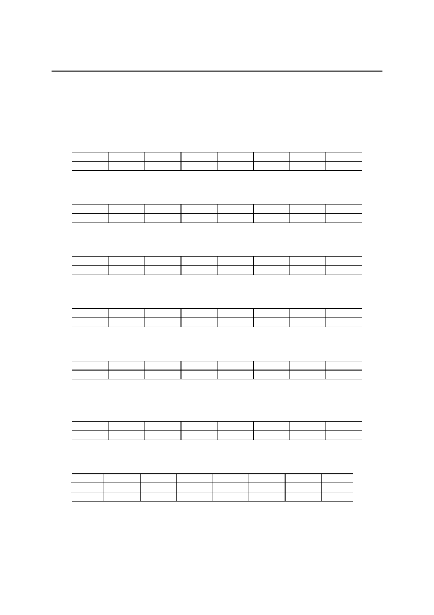
Voice Synthesis Algorithms and Sampling Frequencies during Recording and Playback
The relationships between the voice synthesis algorithms and sampling frequencies available during recording and
playback are shown in Tables 1.1.1 and 1.1.2.
Table 1.1.1 During Recording
f
sam
(kHz)
Voice
synthesis algorithm
4.0 5.3 6.1
6.4
8.0
9.8
10.7
11.6
12.8
14.2 16.0 18.3 21.3
25.6
4-bitADPCM
∞ ∞
∞ ∞ ∞ ∞ ∞ ∞ ∞
◊
◊
◊
◊
◊
4/5/6/7/8-bitADPCM2
∞
∞
∞ ∞ ∞ ∞ ∞ ∞ ∞
◊
◊
◊
◊
◊
2-bitADPCM2
∞
∞
∞ ∞ ∞ ∞ ∞ ∞ ∞
◊
◊
◊
◊
◊
8-bit straight PCM
∞
∞
∞ ∞ ∞ ∞ ∞ ∞ ∞ ∞
∞
∞
∞ ∞
16-bit straight PCM
∞
∞
∞ ∞ ∞ ∞ ∞ ∞ ∞ ∞
∞
∞
◊
◊
8-bit Non-linear PCM
◊
◊
◊
◊
◊
◊
◊
◊
◊
◊
◊
◊
◊
◊
Table 1.1.2 During Playback
f
sam
(kHz)
Voice
synthesis algorithm
4.0 5.3 6.1
6.4
8.0
9.8
10.7
11.6
12.8
14.2 16.0 18.3 21.3
25.6
4-bitADPCM
∞
∞
∞ ∞ ∞ ∞ ∞ ∞ ∞
◊
◊
◊
◊
◊
4/5/6/7/8-bitADPCM2
∞
∞
∞ ∞ ∞ ∞ ∞ ∞ ∞
◊
◊
◊
◊
◊
2-bitADPCM
∞
∞
∞ ∞ ∞ ∞ ∞ ∞ ∞
◊
◊
◊
◊
◊
8-bit straight PCM
∞
∞
∞ ∞ ∞ ∞ ∞ ∞ ∞ ∞
∞
∞
∞ ∞
16-bit straight PCM
∞
∞
∞ ∞ ∞ ∞ ∞ ∞ ∞ ∞
∞
∞
◊
◊
8-bit Non-linear PCM
∞
∞
∞ ∞ ∞ ∞ ∞ ∞ ∞ ∞
∞
∞
◊
◊
FEDL2302DIGEST-05
OKI Semiconductor
ML2302
12/24
Data Configuration
The data configuration of each voice synthesis algorithm is shown in Tables 1.2.1 to 1.2.7.
Table 1.2.1 2-bitADPCM2 Algorithm
D7 D6 D5 D4 D3 D2 D1 D0
MSB1 LSB1 MSB2 LSB2 MSB3 LSB3 MSB4 LSB4
Table 1.2.2 4-bitADPCM Algorithm, 4-bit ADPCM2 Algorithm
D7 D6 D5 D4 D3 D2 D1 D0
MSB1 3SB1 2SB1 LSB1 MSB2 3SB2 2SB2 LSB2
Table 1.2.3 5-bitADPCM2 Algorithm
D7 D6 D5 D4 D3 D2 D1 D0
◊
◊
◊
MSB1 4SB1 3SB1 2SB1 LSB1
Table 1.2.4 6-bitADPCM2 Algorithm
D7 D6 D5 D4 D3 D2 D1 D0
◊
◊
MSB1 5SB1 4SB1 3SB1 2SB1 LSB1
Table 1.2.5 7-bitADPCM2 Algorithm
D7 D6 D5 D4 D3 D2 D1 D0
◊
MSB1 6SB1 5SB1 4SB1 3SB1 2SB1 LSB1
Table 1.2.6 8-bit ADPCM2 Algorithm,
8-bit Non-linear PCM Algorithm, 8-bit straight PCM Algorithm
D7 D6 D5 D4 D3 D2 D1 D0
MSB1 7SB1 6SB1 5SB1 4SB1 3SB1 2SB1 LSB1
Table 1.2.7 16-bit straight PCM Algorithm
D7 D6 D5 D4 D3 D2 D1 D0
MSB1 15SB1 14SB1 13SB1 12SB1 11SB1 10SB1 9SB1
(first)
8SB1 7SB1 6SB1 5SB1 4SB1 3SB1 2SB1 LSB1
(second)
◊: Don't care
FEDL2302DIGEST-05
OKI Semiconductor
ML2302
13/24
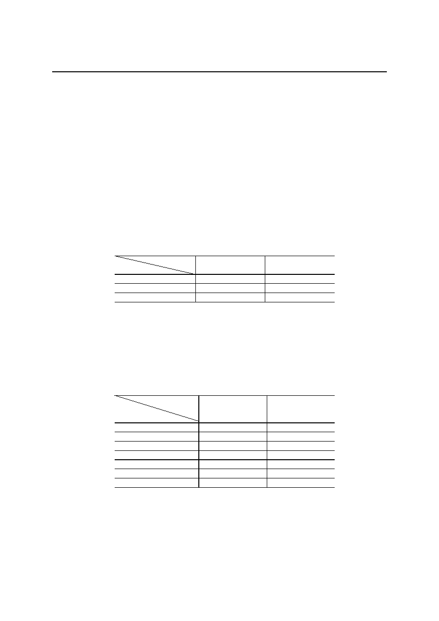
FIFO Memory Configuration
The ML2302 has two FIFO memories; one is for recording and other is for playback.
The configuration of FIFO memory can be changed with a command. Select a FIFO configuration considering
buffering times.
Initially, FIFO memory for recording and FIFO memory for playback each is provided with 1024 bits (128 words
◊ 8 bits).
ML2302 cannot command recording and playback at the same time.
1. Combination of FIFO memory capacities
Table 1.3.1 shows the combination of FIFO memory capacities in recording and playback modes.
Table 1.3.1
Mode
Capacity
Recording Playback
1024 bits
128 w
◊
8 bits
128 w
◊
8 bits
*Initial value
512 bits
64 w
◊
8 bits
64 w
◊
8 bits
256 bits
32 w
◊
8 bits
32 w
◊
8 bits
2. Voice synthesis algorithms and maximum buffering times
Table 1.3.2 shows the maximum buffering times when the FIFO capacity is 1024 bits and the sampling frequency
is 8 kHz.
Table 1.3.2
Mode
Voice
synthesis algorithm
Recording Playback
4-bit OKIADPCM
32 ms
32 ms
4-bit OKIADPCM2
32 ms
32 ms
5/6/7/8-bit OKIADPCM2
16 ms
16 ms
2-bit OKIADPCM2
64 ms
64 ms
8-bit straight PCM
16 ms
16 ms
16-bit straight PCM
8 ms
8 ms
8-bit OKI Non-linear PCM
Note)
16 ms
Note: The 8-bit OKI Non-linear PCM algorithm cannot be used during recording.
FEDL2302DIGEST-05
OKI Semiconductor
ML2302
14/24
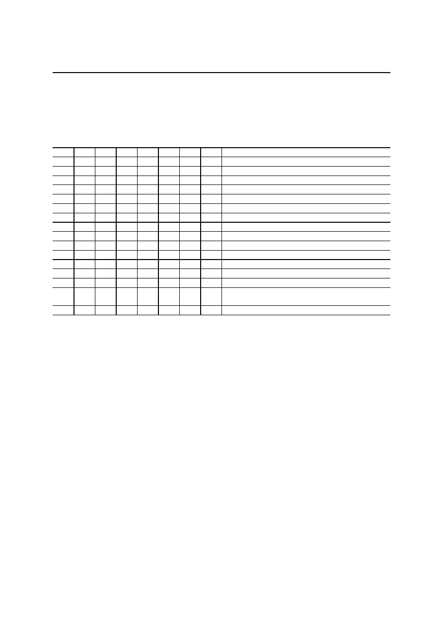
COMMAND LIST
Table 2.1
D7 D6 D5 D4
D3 D2 D1
D0
Function
0 0 0 0 W3
W2 0 0
POWER
DOWN
0 0 0 1 X X X X
Disable
0 0 1 0 S3
S2
S1
S0
Sets
sampling
frequency.
0
0
1
1
C3
C2
C1
C0
RECORDING, PLAYBACK, STOP, PAUSE
0 1 0 0
VH3
VH2
VH1
VH0
Volume
control
1
0 1 0 1
VL3
VL2
VL1
VL0
Volume
control
2
0 1 1 0 0 K2
K1
K0
Level
detection,
noise
injection
0 1 1 1 P3
P2
P1
P0
Voice
synthesis
algorithm
1 0 0 0 R3
R2
R1
0
Analog
specification
1
1 0 0 1 A3
A2
A1
0
Analog
specification
2
1 0 1 0 0 B2
B1
B0
FIFO
memory
byte
configuration
1 0 1 1 F3
F2
F1
0
Signal
output
format
1 1 0 0 G3
G2
G1
G0
DMA
Transfer
1 1 0 1 I3 0 J1 J0
Serial
port
1 1 1 0 U3
U2
U1
U0
Fast Forward/Rewind setting 1 (quick speaking/slow
speaking)
1
1
1
1
Y3
Y2
Y1
Y0
Fast Forward/Rewind setting 2
FEDL2302DIGEST-05
OKI Semiconductor
ML2302
15/24
READING STATUS
The ML2302 supports the following seven status flags.
Table 4.1
Pin Status
Description
D7
Data Recording/Playing flag
High when recording or playback is in progress
D6 Don't
Care
D5
Pause flag
High when playback of left voice is paused
D4 Don't
Care
D3
EMP Information Output flag
Output the same signal as the EMP pin. Note)
D2
MID Information flag
Output the same signal as the MID pin. Note)
D1
FUL Information flag
Output the same signal as the FUL pin. Note)
D0
Data Transfer Error flag
See "Data Transfer Errors".
Note: EM, MID, and FUL are either at the active "H" or at the active "L" by setting the signal output format by
the command. The status signals on D3 to D1 are determined depending on the status of the FIFOST pin as
shown below.
FIFOST = "0"
FIFOST = "1"
D3
EMP signal for playback FIFO
EMP signal for recording FIFO
D2
MID signal for playback FIFO
MID signal for recording FIFO
D1
FUL signal for playback FIFO
FUL signal for recording FIFO
Data Transfer Errors
The Data Transfer flag supports the following four errors.
(1) "H" when data is read while EMP for recording FIFO is "H"
(2) "H" when data is written while FUL for playback FIFO is "H"
(3) "H" when a command is written while
CBUSY is "L".
(4) "H" when recording data cannot be written in FIFO while FUL for recording FIFO is "H".
*These four errors are released when a normal transfer described below is carried out.
(1) Reads data while EMP for recording FIFO is "L".
(2) Writes data while FUL for playback FIFO is "L".
(3) Writes a command while
CBUSY is "H".
(4) The error flag is released when data is written in recording FIFO within LSI after reading data from recording
FIFO and setting FUL for recording FIFO to "L".

FEDL2302DIGEST-05
OKI Semiconductor
ML2302
16/24
ANALOG INPUT AMPLIFIER CIRCUIT
The ML2302 contains two OP amplifiers to amplify a voice signal from a microphone. Each OP amplifier is
provided with the inverting input pin and output pin.
The analog circuit reference voltage SG (signal ground) is input internally to the non-inverting input of each
amplifier.
For amplification, form an inverting amplifier circuit and adjust the amplification ratio by using external resistors.
VLO
V
DD
V
LOUT
(Max)
GND
V
LOUT
(Min)
1/2V
DD
SG
R3 R4
VLO
MIN
MOUT
LIN
LOUT
OP amplifier 1
OP amplifier 2
0.01 µF
0.01 µF
C1
Figure 6.1
The constants of R4 and C1 are determined by f = 1/2
R∑C. C1 is 39.89 pF 39 pF when R4 is 200 k, where the
cut-off frequency of LPF is f = 20 kHz.
During recording, the output VLO of the OP amplifier is input to LPF.
Adjust the amplification ratio by an external resistor so that the output voltage V
LOUT
may be in the
LOUT-permissible input voltage range.
If V
LOUT
is not in this range, the waveform of the LPF output may be deformed.
Table 6.1 shows an examples of LOUT-permissible input voltage ranges of the ML2302.
Table 6.1
LOUT-permissible voltage range V
LOUT
Model name
Supply voltage V
DD
MIN MAX
LOUT-permissible range
ML2302
3 V
0.75 V
2.25 V
1.5 V
pp
The load resistance R
OUTA
of the OP amplifier is 50 k
. Therefore, the feedback resistors R4 and R3 of the
amplifying circuit must be 50 k
or higher.

FEDL2302DIGEST-05
OKI Semiconductor
ML2302
17/24
SPEAKER DRIVING AMPLIFIER
The ML2302 contains two OP amplifiers for driving a speaker; SPOUT≠ which is the inverting type output for a
voice multiplication signal SPIN and SPOUT+ which is the non-inverting type output.
Though SPOUT+ alone can be used, when differential outputs are used, it is possible to gain not only an amplitude
two times that of when a single OP amplifier is used but also a good volume even if a low power supply voltage is
used. The connection diagram of differential outputs are shown below.
Note 1: The gain of a speaker amplifier is determined by R1 and R2.
V (SPOUT≠) = ≠
R2
R1
∑ V(SPIN)
V (SPOUT+) = ≠V(SPOUT≠) =
R2
R1
∑ V(SPIN)
Note 2: C1 is an AC coupling capacitance. The cut-off frequency at a low field is determined by the following
equation.
Select a value of C1 in accordance with a pass band.
f
c
=
1
2
◊
◊
C1
◊
R1
(Hz)
VR
R1
AOUT
SPIN
SPOUT≠
SPOUT+
C1
R2
20 k
20 k
FEDL2302DIGEST-05
OKI Semiconductor
ML2302
18/24
RECORDING TIME AND MEMORY CAPACITY
The recording time of the ML2302 is dependent on the storage capacitance of external memory, the sampling
frequency, and the width of ADPCM bits that have been specified. The recording time of the ML2302 is expressed
by
Recording time =
Memory size (in kbits)
Sampling frequency (kHz)
◊
Width of ADPCM bits
◊
4080
4096
For example, when 8.0 kHz of sampling frequency, 4 bits of ADPCM2, and 8 Mbits of memory size are set, the
recording time is calculated below.
Recording time =
8000
8.0
◊
4
= 249 seconds = 4 minutes 9 seconds
◊
4080
4096
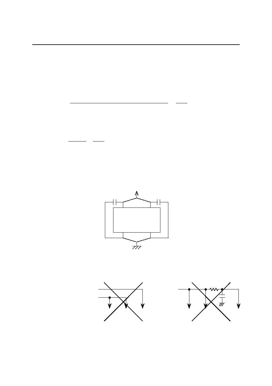
CONNECTION OF POWER SUPPLY
The ML2302 contains a single power supply as shown in Figure 7.1.
The power supply is connected to the analog unit and digital unit separately.
Figure 7.1
Avoid following power supply connections.
DV
DD
Power supply for the analog circuit
Power supply for the digital circuit
DV
DD
AV
DD
DV
DD
Power supply
DV
DD
AV
DD
Figure 7.2
ML2302
DV
DD
DGND
AV
DD
AGND

FEDL2302DIGEST-05
OKI Semiconductor
ML2302
19/24
APPLICATION CIRCUIT EXAMPLE
(1) MCU and External Interface
Memory
MCU
ML2302
D7~0
DREQL
DACKL
IOW
IOR
RD
WR
CS
D/
C
CH
EMP
MID
FUL
VOXO
FIFOST
SIOCK
VCK
DASD
ADSD
CBUSY
BUSY
RESET
TEST2
TEST3
TEST4
TEST5
TEST6
TEST7
TEST9
TEST0
TEST8
SPOUT
SPOUT-
SPIN
AOUT
MIN
MOUT
LIN
LOUT
CB1
CB2
VR
SPVDD
SG
XT
XT
DV
DD
AV
DD
AV
DD
(SP)
DGND
AGND
AGND(SP)

FEDL2302DIGEST-05
OKI Semiconductor
ML2302
20/24
(2) Interface when DMA controller is Used
Memory
MCU
DMA
controller
ML2302
D7~0
DREQL
DACKL
IOW
IOR
RD
WR
CS
D/
C
CH
EMP
MID
FUL
VOXO
FIFOST
SIOCK
VCK
DASD
ADSD
CBUSY
BUSY
RESET
TEST2
TEST3
TEST4
TEST5
TEST6
TEST7
TEST9
TEST0
TEST8
SPOUT
SPOUT-
SPIN
AOUT
MIN
MOUT
LIN
LOUT
CB1
CB2
VR
SPVDD
SG
XT
XT
DV
DD
AV
DD
AV
DD
(SP)
DGND
AGND
AGND(SP)

FEDL2302DIGEST-05
OKI Semiconductor
ML2302
21/24
PACKAGE DIMENSIONS
TQFP64-P-1010-0.50-K
Mirror finish
Package material
Epoxy resin
Lead frame material
42 alloy
Pin treatment
Solder plating (
5µm)
Package weight (g)
0.26 TYP.
5
Rev. No./Last Revised
4/Oct. 28, 1996
Notes for Mounting the Surface Mount Type Package
The surface mount type packages are very susceptible to heat in reflow mounting and humidity absorbed in storage.
Therefore, before you perform reflow mounting, contact Oki's responsible sales person for the product name,
package name, pin number, package code and desired mounting conditions (reflow method, temperature and
times).
(Unit: mm)

FEDL2302DIGEST-05
OKI Semiconductor
ML2302
22/24
P-VFLGA71-6.2x6.5-0.65-W
Package material
Epoxy resin
Ball material
Sn/Pb
Package weight (g)
0.03 TYP.
5
Rev. No./Last Revised
2/Oct. 31, 2000
Notes for Mounting the Surface Mount Type Package
The surface mount type packages are very susceptible to heat in reflow mounting and humidity absorbed in storage.
Therefore, before you perform reflow mounting, contact Oki's responsible sales person for the product name,
package name, pin number, package code and desired mounting conditions (reflow method, temperature and
times).
(Unit: mm)

FEDL2302DIGEST-05
OKI Semiconductor
ML2302
23/24
REVISION HISTORY
Page
Document
No.
Date
Previous
Edition
Current
Edition
Description
FEDL2302DIGEST-01
Apr. 2001
≠
≠
Final edition 1
FEDL2302DIGEST-02
Apr. 3, 2003
≠
≠
Final edition 2
FEDL2302DIGEST-03
May 30, 2003
≠
≠
Final edition 3
1 1
Partially changed contents of the
"FEATURES" section.
2
2
Modified the block diagram.
FEDL2302DIGEST-04
Jan. 20, 2004
≠ 10-18
Added
pages.
6
6
Partially corrected the Pin Descriptions.
FEDL2302DIGEST-05
Dec. 27, 2004
19
19,20
Modified the application circuit example.

FEDL2302DIGEST-05
OKI Semiconductor
ML2302
24/24
NOTICE
1. The information contained herein can change without notice owing to product and/or technical improvements.
Before using the product, please make sure that the information being referred to is up-to-date.
2. The outline of action and examples for application circuits described herein have been chosen as an explanation
for the standard action and performance of the product. When planning to use the product, please ensure that the
external conditions are reflected in the actual circuit, assembly, and program designs.
3. When designing your product, please use our product below the specified maximum ratings and within the
specified operating ranges including, but not limited to, operating voltage, power dissipation, and operating
temperature.
4. Oki assumes no responsibility or liability whatsoever for any failure or unusual or unexpected operation
resulting from misuse, neglect, improper installation, repair, alteration or accident, improper handling, or
unusual physical or electrical stress including, but not limited to, exposure to parameters beyond the specified
maximum ratings or operation outside the specified operating range.
5. Neither indemnity against nor license of a third party's industrial and intellectual property right, etc. is granted
by us in connection with the use of the product and/or the information and drawings contained herein. No
responsibility is assumed by us for any infringement of a third party's right which may result from the use
thereof.
6. The products listed in this document are intended for use in general electronics equipment for commercial
applications (e.g., office automation, communication equipment, measurement equipment, consumer
electronics, etc.). These products are not, unless specifically authorized by Oki, authorized for use in any
system or application that requires special or enhanced quality and reliability characteristics nor in any system
or application where the failure of such system or application may result in the loss or damage of property, or
death or injury to humans.
Such applications include, but are not limited to, traffic and automotive equipment, safety devices, aerospace
equipment, nuclear power control, medical equipment, and life-support systems.
7. Certain products in this document may need government approval before they can be exported to particular
countries. The purchaser assumes the responsibility of determining the legality of export of these products and
will take appropriate and necessary steps at their own expense for these.
8. No part of the contents contained herein may be reprinted or reproduced without our prior permission.
Copyright 2004 Oki Electric Industry Co., Ltd.