 | –≠–ª–µ–∫—Ç—Ä–æ–Ω–Ω—ã–π –∫–æ–º–ø–æ–Ω–µ–Ω—Ç: ML63187B | –°–∫–∞—á–∞—Ç—å:  PDF PDF  ZIP ZIP |

FEDL63187B-06
1Semiconductor
This version: Sep. 2001
Previous version: Mar. 2000
ML63187B/63189B
4-Bit Microcontroller with Built-in1024-Dot Matrix LCD Drivers and Melody Circuit,
Operating at 0.9 V (Min.)
1/36
GENERAL DESCRIPTION
The ML63187B and ML63189B are CMOS 4-bit microcontroller with built-in 1024-dot matrix LCD drivers and
operates at 0.9 V (min.). The ML63187B and 63189B are suitable for applications such as games, toys, watches,
etc. which are provided with an LCD display.
The ML63187B and ML63189B are M6318x series mask ROM-version product of OLMS-63K family, which
employs Oki's original CPU core nX-4/250.
FEATURES
∑
Rich instruction set
408 instructions
Transfer, rotate, increment/decrement, arithmetic operations, comparison, logic operations, mask
operations, bit operations, ROM table reference, stack operations, flag operations, branch, conditional
branch, call/return, control
∑
Rich selection of addressing modes
Indirect addressing of four data memory types, with current bank register, extra bank register, HL register
and XY register
Data memory bank internal direct addressing mode
∑
Processing speed
Two clocks per machine cycle, with most instructions executed in one machine cycle
Minimum instruction execution time
: 61
µ
s (@32.768 kHz system clock)
1
µ
s (@2 MHz system clock)
∑
Clock generation circuit
Low-speed clock
: Crystal oscillation or RC oscillation selected with mask option
(30 to 80 kHz)
High-speed clock
: Ceramic oscillation or RC oscillation selected with software
(2 MHz max.)
∑
Program memory space
∑ ML63187B : 16 K words
∑ ML63189B : 32 K words
Basic instruction length is 16 bits/1 word
∑
Data memory space
∑ ML63187B : 1024 nibbles
∑ ML63189B : 1536 nibbles
∑
Stack level
Call stack level
: 16 levels
Register stack level
: 16 levels
FEDL63187B-06
1Semiconductor
ML63187B/63189B
2/36
∑
I/O ports
Input ports:
Selectable as input with pull-up resistor/input with pull-down resistor/high-impedance
input
Input-output ports: Selectable as input with pull-up resistor/input with pull-down resistor/high-impedance
input
Selectable as P-channel open drain output/N-channel open drain output/CMOS
output/high-impedance output
Can be interfaced with external peripherals that use a different power supply than this device uses. V
DD
is the
power supply pin for ports.
Number of ports:
ML63187B
Input-output port
: 2 ports
◊
4 bits
ML63189B
Input port
: 1 port
◊
4 bits
Input-output port
: 4 ports
◊
4 bits
∑
Melody output
Melody frequency
: 529 to 2979 Hz
Tone length
: 63 types
Tempo
: 15 types
Melody data
: Resides in the program memory
Buzzer driver signal output
: 4 kHz
∑
LCD driver
Number of segments
: 1024 Max. (64 SEG
◊
16 COM)
Duty
: 1/1 to 1/16 duty
Bias
: Selectable as 1/4 or 1/5 bias
regulator circuit built-in
Frame frequency
: 64 Hz (at 1/16 duty) , 128 Hz (at 1/8 duty ) , 256 Hz (at 1/4 duty) ,
512Hz (at 1/2 duty) , 1024 Hz (at 1/1 duty )
Contrast
: A maximum of 16 levels adjustable
Display modes
: Selectable s all-ON mode/all-OFF mode/power down mode/normal
display mode adjustable contrast.
∑
System reset function
∑
System reset by RESET pin (Built-in 2 kHz RESET sampling circuit can be selected by mask option)
∑
System reset by power-on detection (When not using 2 kHz RESET sampling circuit)
∑
System reset by detection that low-speed clock has stopped oscillation
∑
Battery check
Low-voltage supply check
The value of the judgment voltage is selected by the software by setting the LD1 and LD0 bits of BLDCON.
LD1
LD0
Judgment Voltage (V)
Remarks
0
0
1.05
±
0.10
Ta = 25
∞
C
0
1
1.20
±
0.10
Ta = 25
∞
C
1
0
1.80
±
0.10
Ta = 25
∞
C
1
1
2.40
±
0.10
Ta = 25
∞
C
∑
Power supply backup
Backup circuit (voltage multiplier) enables operation at 0.9 V minimum

FEDL63187B-06
1Semiconductor
ML63187B/63189B
3/36
∑
Timers and counter
8-bit timer
◊
4
Selectable as auto-reload mode/capture mode/clock frequency measurement mode
Watchdog timer
◊
1
100 Hz timer
◊
1
Measurable in steps of 1/100 sec.
15-bit time base counter
◊
1
1, 2, 4, 8, 16, 32, 64, and 128 Hz signals can be read
∑
Shift register
Shift clock
: 1
◊
or 1/2
◊
system clock, timer 1 overflow, external clock
Data length
: 8 bits
∑
Interrupt sources
ML63187B
External interrupt
: 2
Internal interrupt
: 12 (watchdog timer interrupt is a nonmaskable interrupt)
ML63189B
External interrupt
: 3
Internal interrupt
: 12 (watchdog timer interrupt is a nonmaskable interrupt)
∑
Operating temperature
≠20 to +70
∞
C
∑
Operating voltage
When backup used
: 0.9 to 2.7 V
(Operating frequency: 30 to 80 kHz)
1.2 to 2.7 V
(Operating frequency: 300 to 500 kHz)
1.5 to 2.7 V
(Operating frequency: 200 kHz to 1 MHz)
When backup not used
: 1.8 to 5.5 V
(Operating frequency: 200 kHz to 2 MHz)
∑
Package:
Chip (ML63187B: 111 pads , ML63189B: 123 pads): (Product name: ML63187B-xxxWA,
ML63189B-xxxWA)
128-pin plastic QFP (QFP128-P-1420-0.50-K)
: (Product name: ML63187B-xxxGA,
ML63189B-xxxGA)
xxx indicates a code number.
FEDL63187B-06
1Semiconductor
ML63187B/63189B
4/36
MASK OPTION
In the ML63187B and ML63189B use the mask option to specify the following functions:
∑
Low-Speeed clock oscillation circuit
Specify the crystal oscillation circuit or the RC oscillation circuit for the low-speed clock oscillation
circuit.
∑
Reset signal sampling
Specify whether or not the reset signal will be sampled at 2 kHz.
When specifying "will carry out 2 kHz sampling," hold the RESET pin at a "H" level for 1 ms or more.
To use the mask option, assign mask option data in the application program in accordance with the formats below.
The mask option area for each device is an application program execution disabled area.
Mask Option Data Assignment Format
Function
Mask option area
bit
data
Option to be selected
0
Crystal oscillation circuit
Low-speed clock oscillation circuit
(crystal oscillation circuit/RC oscillation circuit)
ML63187B:3FE0H bit 0
1
RC oscillation circuit
0
Will carry out 2 kHz sampling
Reset signal sampling
(will/will not carry out 2 kHz sampling)
ML63189B:7FE0H bit 1
1
Will not carry out 2 kHz sampling

FEDL63187B-06
1Semiconductor
ML63187B/63189B
5/36
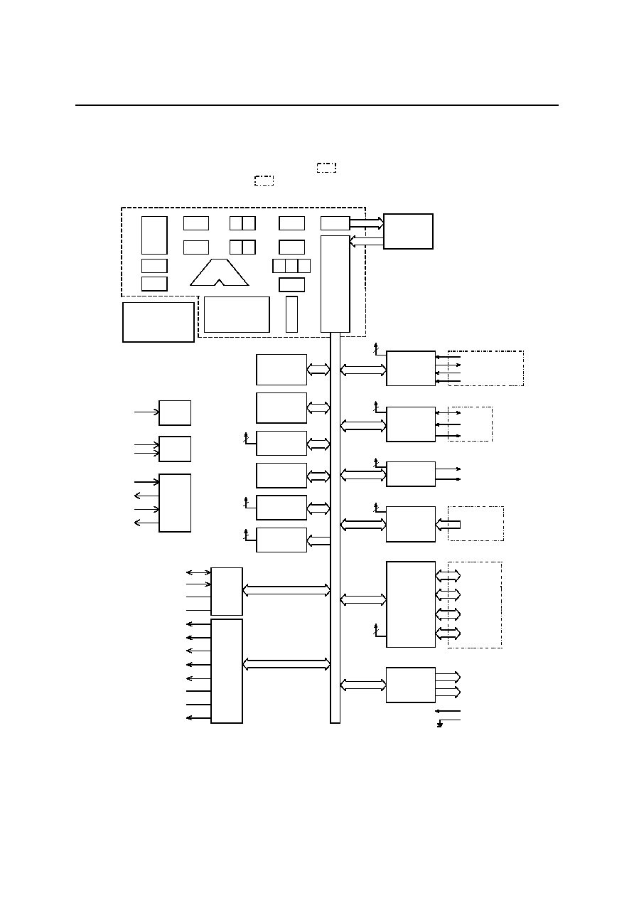
BLOCK DIAGRAM (ML63187B)
An asterisk (
*
) indicates the port secondary function. indicates that the power is supplied to the circuits
corresponding to the signal names inside from V
DDI
(power supply for interface).
ROM
16 KW
BUS
CON-
TROL
MIE
XT0
XT1
OSC0
OSC1
OSC
CBR
EBR
L
C
G Z
ALU
RA
A
IR
INSTRUCTION
DECODER
RAM
1024N
nX-4/250
RESET
RST
V
DD1
PC
H
Y
X
TIMING
CON-
TROL
SP
RSP
STACK
CAL : 16-level
REG : 16-level
TIMER
8 bit
◊
4
SCLK*
SIN*
SOUT*
4
INT
SFT
TM0CAP/TM1CAP*
TM0OVF/TM1OVF*
T02CK*
T13CK*
1
INT
I/O
PORT
PB.0-PB.3
PE.0-PE.3
2
INT
V
DDH
V
DD
CB1
CB2
DA
T
A
BU
S
TBC
4
INT
BLD
INT
100 HzTC
1
BACK
UP
V
SS
MELODY
MD
1
INT
MDB
LCD
&
DSPR
COM1-16
SEG0-63
TST1
TST
TST2
INT
WDT
1
V
DD1
V
DD2
V
DD3
V
DD4
V
DD5
C1
C2
V
DDL
BIAS
INT187
CPU CORE
FEDL63187B-06
1Semiconductor
ML63187B/63189B
6/36
BLOCK DIAGRAM (ML63189B)
An asterisk (
*
) indicates the port secondary function. indicates that the power is supplied to the circuits
corresponding to the signal names inside from V
DDI
(power supply for interface).
ROM
32 KW
BUS
CON-
TROL
MIE
XT0
XT1
OSC0
OSC1
OSC
CBR
EBR
L
C
G
Z
ALU
RA
A
IR
INSTRUCTION
DECODER
RAM
1536N
nX-4/250
RESET
RST
V
DDI
PC
H
Y
X
TIMING
CON-
TROL
SP
RSP
STACK
CAL : 16-level
REG : 16-level
TIMER
8 bit
◊
4
SCLK*
SIN*
SOUT*
4
INT
SFT
TM0CAP/TM1CAP*
TM0OVF/TM1OVF*
T02CK*
T13CK*
1
INT
I/O
PORT
P9.0-P9.3
PA.0-PA.3
PB.0-PB.3
PE.0-PE.3
2
INT
V
DDH
V
DD
CB1
CB2
DA
T
A
BU
S
TBC
4
INT
BLD
INT
100 HzTC
1
BACK
UP
V
SS
MELODY
MD
1
INT
MDB
1
INT
INPUT
PORT
P0.0-P0.3
LCD
&
DSPR
COM1-16
SEG0-63
TST1
TST
TST2
INT
WDT
1
V
DD1
V
DD2
V
DD3
V
DD4
V
DD5
C1
C2
V
DDL
BIAS
INT189
CPU CORE
FEDL63187B-06
1Semiconductor
ML63187B/63189B
7/36
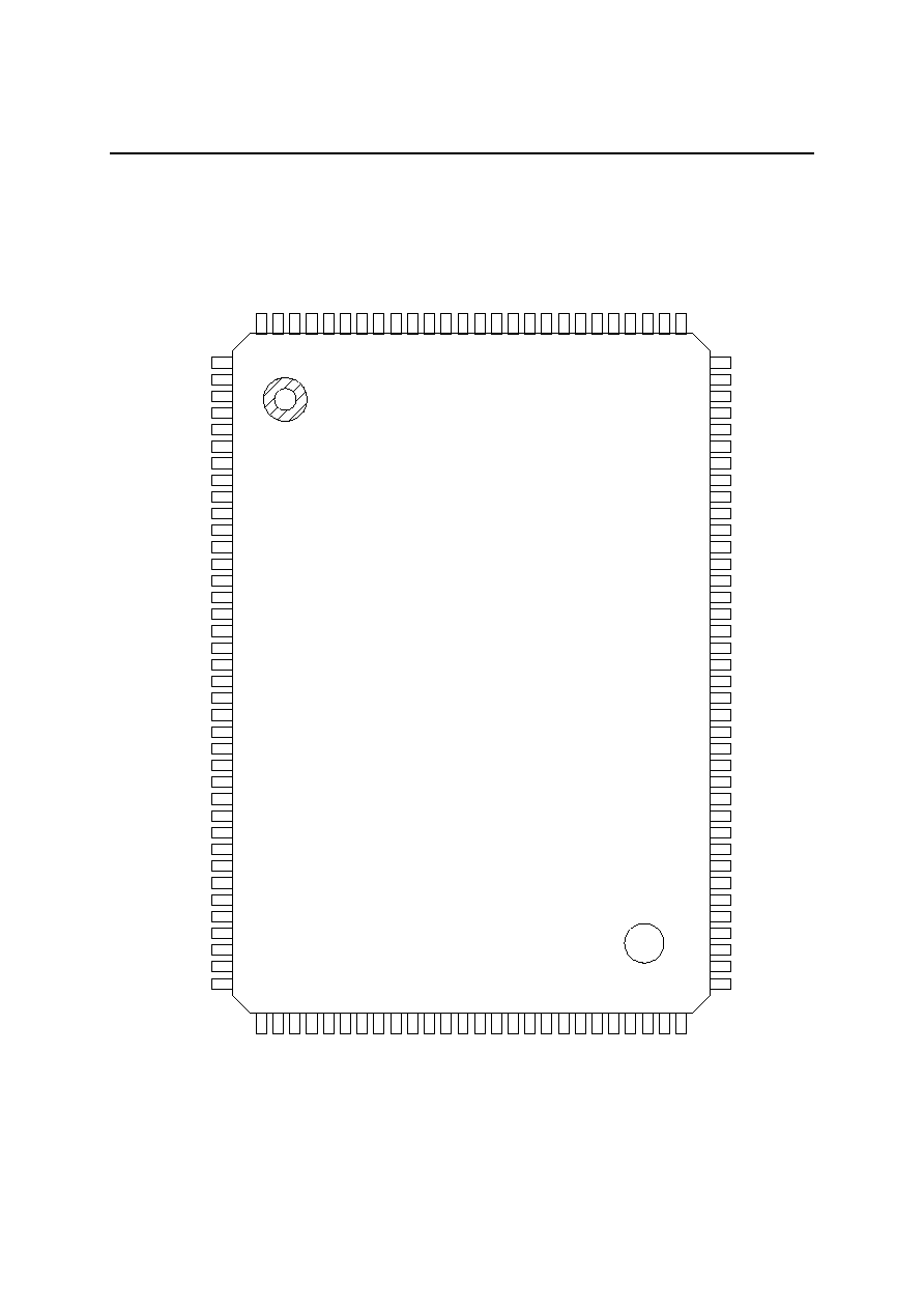
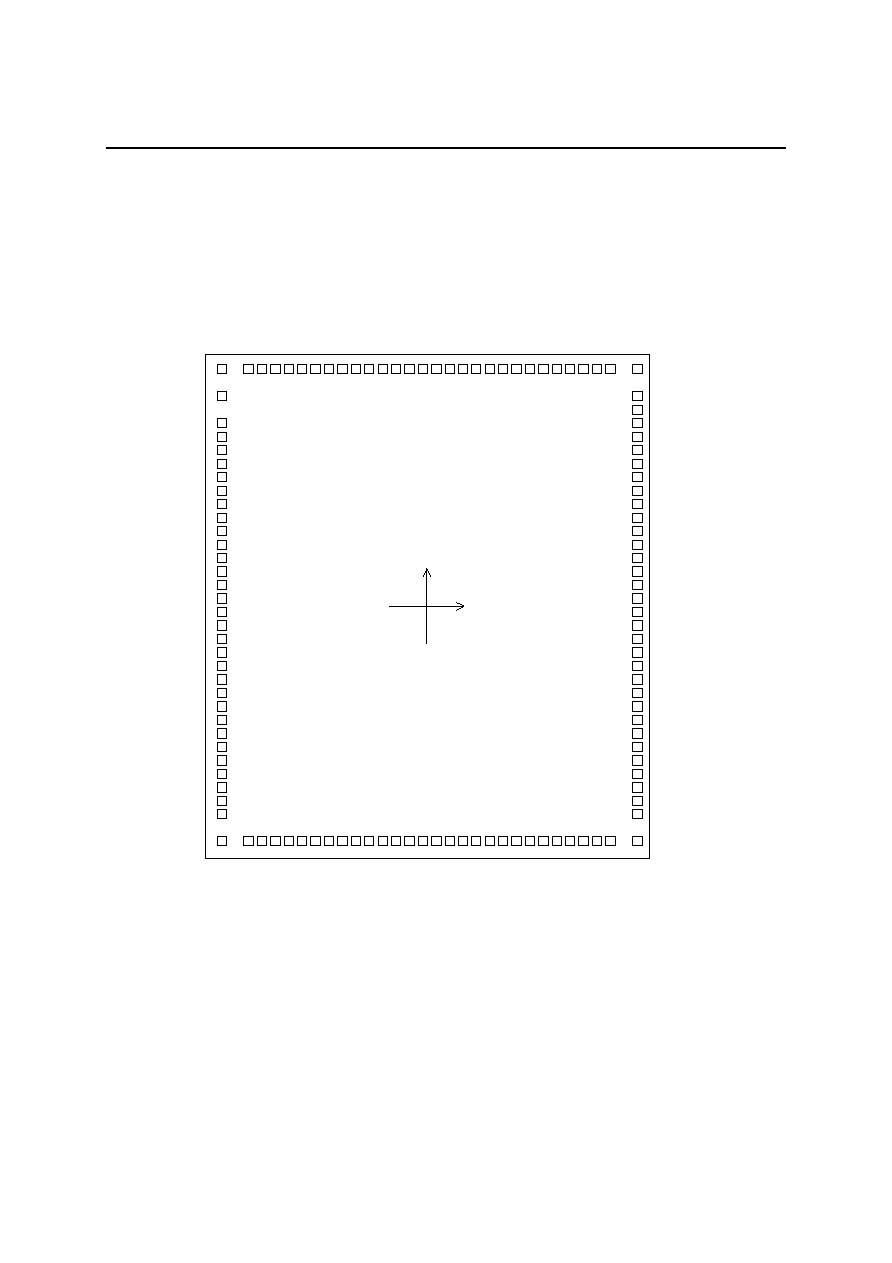
PIN CONFIGURATION (TOP VIEW) (ML63187B)
128-Pin Plastic QFP
Note:
Pins marked as (NC) are no-connection pins which are left open.
1
2
3
4
5
6
7
8
9
10
11
12
13
14
15
16
17
18
19
20
21
22
23
24
25
26
27
28
29
30
(NC)
(NC)
(NC)
(NC)
SEG38
SEG39
SEG40
SEG41
SEG42
SEG43
SEG44
SEG45
SEG46
SEG47
SEG48
SEG49
SEG50
SEG51
SEG52
SEG53
SEG54
SEG55
SEG56
SEG57
SEG58
SEG59
SEG60
SEG61
SEG62
SEG63
57
56
55
54
53
52
51
50
49
48
47
46
45
44
43
42
41
40
39
RE
S
E
T
OS
C0
OS
C1
V
DDL
V
DD
CB
2
CB
1
V
DDH
C2
C1
V
DD5
V
DD4
V
DD3
V
DD2
V
DD1
V
SS
COM
1
6
COM
1
5
COM
1
4
COM
1
3
102
101
100
99
98
97
96
95
94
93
92
91
90
89
88
87
86
85
84
83
82
81
80
79
78
77
76
75
74
73
(NC)
(NC)
(NC)
(NC)
SEG11
SEG10
SEG9
SEG8
SEG7
SEG6
SEG5
SEG4
SEG3
SEG2
SEG1
SEG0
COM8
COM7
COM6
COM5
COM4
COM3
COM2
COM1
PB.3
PB.2
PB.1
PB.0
PE.3
PE.2
SEG
1
8
SEG
1
9
SEG
2
0
SEG
2
1
SEG
2
2
SEG
2
3
SEG
2
4
SEG
2
5
SEG
2
6
SEG
2
7
SEG
2
8
SEG
2
9
SEG
3
0
SEG
3
1
SEG
3
2
SEG
3
3
SEG
3
4
SEG
3
5
SEG
3
6
SEG
3
7
109
11
0
111
11
2
11
3
11
4
11
5
11
6
11
7
11
8
11
9
120
121
122
123
124
125
126
127
128
31
32
33
34
35
36
37
38
COM9
COM10
COM11
COM12
(NC)
(NC)
(NC)
(NC)
72
71
70
69
68
67
66
65
PE.1
PE.0
V
DDI
(NC)
(NC)
(NC)
(NC)
(NC)
64
63
62
61
60
59
MD
B
MD
TST2
TST1
XT
0
XT
1
SEG
1
2
SEG
1
3
SEG
1
4
SEG
1
5
SEG
1
6
SEG
1
7
103
104
105
106
107
108
58
FEDL63187B-06
1Semiconductor
ML63187B/63189B
8/36
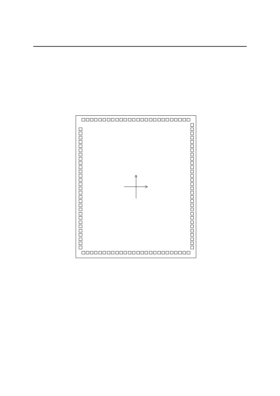
PAD CONFIGURATION (ML63187B)
Pad Layout
Chip size
: 4.238 mm
◊
4.914 mm
Chip thickness
: 350
µ
m (280
µ
m: available as required)
Coordinate origin
: center of chip
Pad hole size
: 100
µ
m
◊
100
µ
m
Pad size
: 110
µ
m
◊
110
µ
m
Minimum pad pitch : 140
µ
m
Note: The chip substrate voltage is V
SS
.
27 SEG38
28 SEG39
SEG11 111
29 SEG40
SEG10 110
30 SEG41
SEG9 109
31 SEG42
SEG8 108
32 SEG43
SEG7 107
33 SEG44
SEG6 106
34 SEG45
SEG5 105
35 SEG46
SEG4 104
36 SEG47
SEG3 103
37 SEG48
SEG2 102
38 SEG49
SEG1 101
39 SEG50
SEG0 100
40 SEG51
COM8 99
41 SEG52
COM7 98
42 SEG53
COM6 97
43 SEG54
COM5 96
44 SEG55
COM4 95
45 SEG56
COM3 94
46 SEG57
COM2 93
47 SEG58
COM1 92
48 SEG59
PB.3 91
49 SEG60
PB.2 90
50 SEG61
PB.1 89
SEG
30 19
SEG
29 18
57 CO
M
1
3
SEG
28 17
58 CO
M
1
4
SEG
27 16
59 CO
M
1
5
SEG
26 15
60 CO
M
1
6
SEG
25 14
61 V
SS
SEG
24 13
62 V
DD1
SEG
23 12
63 V
DD2
SEG22 1
1
64 V
DD3
SEG
21 10
65 V
DD4
SEG
20 9
66 V
DD5
67 C1
68 C2
69 V
DDH
70 CB1
71 CB2
SEG
14 3
72 V
DD
SEG
13 2
73 V
DDL
SEG
12 1
74 O
S
C1
75 O
S
C0
76 RESET
77 X
T
1
78 X
T
0
79 T
S
T
1
80 T
S
T
2
81 M
D
82 M
D
B
SEG
37 26
SEG
36 25
SEG
35 24
SEG
34 23
SEG
33 22
SEG
32 21
SEG
31 20
51 SEG62
PB.0 88
52 SEG63
PE.3 87
53 COM9
PE.2 86
54 COM10
PE.1 85
55 COM11
PE.0 84
56 COM12
V
DDI
83
M
L63187
SEG
17 6
SEG
16 5
SEG
15 4
SEG
19 8
SEG
18 7
Y
X
(0,0)

FEDL63187B-06
1Semiconductor
ML63187B/63189B
9/36
Pad Coordinates (ML63187B)
Center of chip: X = 0, Y = 0
Pad No. Pad Name X (
µ
m) Y (
µ
m) Pad No. Pad Name X (
µ
m) Y (
µ
m) Pad No. Pad Name X (
µ
m) Y (
µ
m)
1
SEG12
≠1755 ≠2311
42
SEG53
1969
70
83
V
DDI
≠1969 1895
2
SEG13
≠1615 ≠2311
43
SEG54
1969
211
84
PE.0
≠1969 1755
3
SEG14
≠1474 ≠2311
44
SEG55
1969
351
85
PE.1
≠1969 1615
4
SEG15
≠1334 ≠2311
45
SEG56
1969
491
86
PE.2
≠1969 1474
5
SEG16
≠1193 ≠2311
46
SEG57
1969
632
87
PE.3
≠1969 1334
6
SEG17
≠1053 ≠2311
47
SEG58
1969
772
88
PB.0
≠1969 1193
7
SEG18
≠913 ≠2311
48
SEG59
1969
913
89
PB.1
≠1969 1053
8
SEG19
≠772 ≠2311
49
SEG60
1969 1053
90
PB.2
≠1969
913
9
SEG20
≠632 ≠2311
50
SEG61
1969 1193
91
PB.3
≠1969
772
10
SEG21
491 ≠2311
51
SEG62
1969 1334
92
COM1
≠1969
632
11
SEG22
≠351 ≠2311
52
SEG63
1969
l 474
93
COM2
≠1969
491
12
SEG23
≠211 ≠2311
53
COM9
1969 1615
94
COM3
≠1969
351
13
SEG24
≠70 ≠2311
54
COM10
1969 1755
95
COM4
≠1969
211
14
SEG25
70 ≠2311
55
COM11
1969 1895
96
COM5
≠1969
70
15
SEG26
211 ≠2311
56
COM12
1969 2036
97
COM6
≠1969
≠70
16
SEG27
351 ≠2311
57
COM13
1755 2311
98
COM7
≠1969 ≠211
17
SEG28
491 ≠2311
58
COM14
1615 2311
99
COM8
≠1969 ≠351
18
SEG29
632 ≠2311
59
COM15
1474 2311
100
SEG0
≠1969 ≠491
19
SEG30
772 ≠2311
60
COM16
1334 2311
101
SEG1
≠1969 ≠632
20
SEG31
913 ≠2311
61
V
SS
1193 2311
102
SEG2
≠1969 ≠772
21
SEG32
1053 ≠2311
62
V
DD1
1053 2311
103
SEG3
≠1969 ≠913
22
SEG33
1193 ≠2311
63
V
DD2
913 2311
104
SEG4
≠1969 ≠1053
23
SEG34
1334 ≠2311
64
V
DD3
772 2311
105
SEG5
≠1969 ≠1193
24
SEG35
1474 ≠2311
65
V
DD4
632 2311
106
SEG6
≠1969 ≠1334
25
SEG36
1615 ≠2311
66
V
DD5
491 2311
107
SEG7
≠1969 ≠1474
26
SEG37
1755 ≠2311
67
C1
351 2311
108
SEG8
≠1969 ≠1615
27
SEG38
1969 ≠2036
68
C2
211 2311
109
SEG9
≠1969 ≠1755
28
SEG39
1969 ≠1895
69
V
DDH
70 2311
110
SEG10
≠1969 ≠1895
29
SEG40
1969 ≠1755
70
CB1
≠70 2311
111
SEG11
≠1969 ≠2036
30
SEG41
1969 ≠1615
71
CB2
≠211 2311
31
SEG42
1969 ≠1474
72
V
DD
≠351 2311
32
SEG43
1969 ≠1334
73
V
DDL
≠491 2311
33
SEG44
1969 ≠1193
74
OSC1
≠632 2311
34
SEG45
1969 ≠1053
75
OSC0
≠772 2311
35
SEG46
1969
≠913
76
RESET
≠913 2311
36
SEG47
1969
≠772
77
XT1
≠1053 2311
37
SEG48
1969
≠632
78
XT0
≠1193 2311
38
SEG49
1969
491
79
TST1
≠1334 2311
39
SEG50
1969
≠351
80
TST2
≠1474 2311
40
SEG51
1969
≠211
81
MD
≠1615 2311
41
SEG52
1969
≠70
82
MDB
≠1755 2311
FEDL63187B-06
1Semiconductor
ML63187B/63189B
10/36
PIN CONFIGURATION (TOP VIEW) (ML63189B)
128-Pin Plastic QFP
Note:
Pins marked as (NC) are no-connection pins which are left open.
58
1
2
3
4
5
6
7
8
9
10
11
12
13
14
15
16
17
18
19
20
21
22
23
24
25
26
27
28
29
30
(NC)
SEG30
SEG31
SEG32
SEG33
SEG34
SEG35
SEG36
SEG37
SEG38
SEG39
SEG40
SEG41
SEG42
SEG43
SEG44
SEG45
SEG46
SEG47
SEG48
SEG49
SEG50
SEG51
SEG52
SEG53
SEG54
SEG55
SEG56
SEG57
SEG58
57
56
55
54
53
52
51
50
49
48
47
46
45
44
43
42
41
40
39
OS
C1
V
DDL
V
DD
CB
2
CB
1
V
DDH
C2
C1
V
DD5
V
DD4
V
DD3
V
DD2
V
DD1
V
SS
COM
1
6
COM
1
5
COM
1
4
COM
1
3
COM
1
2
COM
1
1
102
101
100
99
98
97
96
95
94
93
92
91
90
89
88
87
86
85
84
83
82
81
80
79
78
77
76
75
74
73
(NC)
SEG3
SEG2
SEG1
SEG0
COM8
COM7
COM6
COM5
COM4
COM3
COM2
COM1
P0.3
P0.2
P0.1
P0.0
P9.3
P9.2
P9.1
P9.0
PA.3
PA.2
PA.1
PA.0
PB.3
PB.2
PB.1
PB.0
PE.3
SEG
1
0
SEG
1
1
SEG
1
2
SEG
1
3
SEG
1
4
SEG
1
5
SEG
1
6
SEG
1
7
SEG
1
8
SEG
1
9
SEG
2
0
SEG
2
1
SEG
2
2
SEG
2
3
SEG
2
4
SEG
2
5
SEG
2
6
SEG
2
7
SEG
2
8
SEG
2
9
109
11
0
111
11
2
11
3
11
4
11
5
11
6
11
7
11
8
11
9
120
121
122
123
124
125
126
127
128
31
32
33
34
35
36
37
38
SEG59
SEG60
SEG61
SEG62
SEG63
COM9
COM10
(NC)
72
71
70
69
68
67
66
65
PE.2
PE.1
PE.0
V
DDI
(NC)
MDB
MD
(NC)
64
63
62
61
60
59
TST2
TST1
XT
0
XT
1
R
ESE
T
OS
C0
SEG
4
SEG
5
SEG
6
SEG
7
SEG
8
SEG
9
103
104
105
106
107
108
FEDL63187B-06
1Semiconductor
ML63187B/63189B
11/36
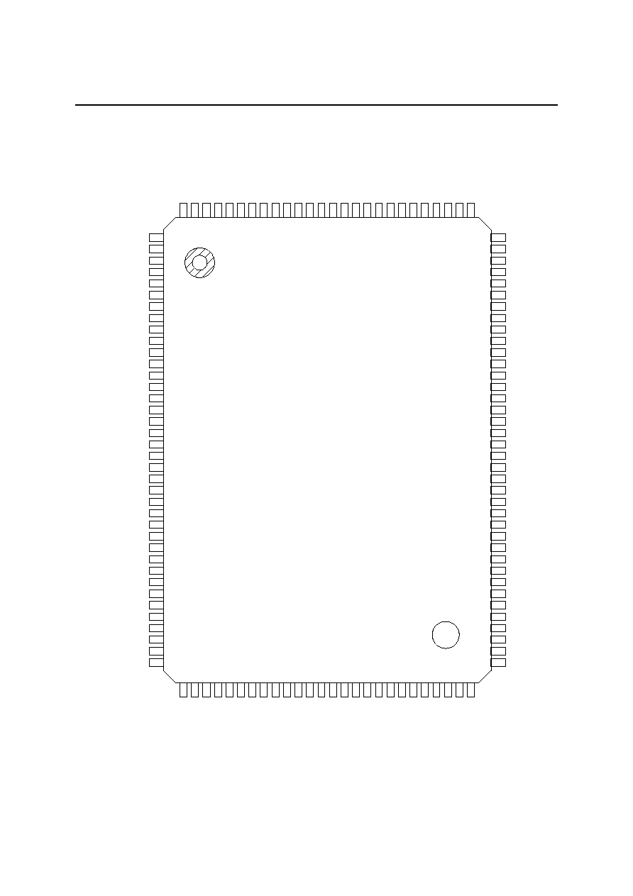
PAD CONFIGURATION (ML63189B)
Pad Layout
Chip size
: 4.81 mm
◊
5.20 mm
Chip thickness
: 350
µ
m (280
µ
m: available as required)
Coordinate origin
: center of chip
Pad hole size
: 100
µ
m
◊
100
µ
m
Pad size
: 110
µ
m
◊
110
µ
m
Minimum pad pitch : 140
µ
m
Note: The chip substrate voltage is V
SS
.
64 C
O
M
1
0
31 SEG32
SEG1 123
92 M
D
B
SEG
2 1
63 C
O
M
9
SEG
31 30
32 SEG33
SEG0 122
33 SEG34
COM8 121
34 SEG35
COM7 120
35 SEG36
COM6 119
36 SEG37
COM5 118
37 SEG38
COM4 117
38 SEG39
COM3 116
39 SEG40
COM2 115
40 SEG41
COM1 114
41 SEG42
P0.3 113
42 SEG43
P0.2 112
43 SEG44
P0.1 111
44 SEG45
P0.0 110
45 SEG46
P9.3 109
46 SEG47
P9.2 108
47 SEG48
P9.1 107
48 SEG49
P9.0 106
49 SEG50
PA.3 105
50 SEG51
PA.2 104
51 SEG52
PA.1 103
52 SEG53
PA.0 102
53 SEG54
PB.3 101
54 SEG55
PB.2 100
55 SEG56
PB.1 99
56 SEG57
PB.0 98
57 SEG58
PE.3 97
58 SEG59
PE.2 96
59 SEG60
PE.1 95
60 SEG61
PE.0 94
61 SEG62
62 SEG63
V
DDI
93
SEG
30 29
65 C
O
M
1
1
SEG
29 28
66 C
O
M
1
2
SEG
28 27
67 C
O
M
1
3
SEG
27 26
68 C
O
M
1
4
SEG
26 25
69 C
O
M
1
5
SEG
25 24
70 C
O
M
1
6
SEG
24 23
71 V
SS
SEG
23 22
72 V
DD1
SEG
22 21
73 V
DD2
SEG
21 20
74 V
DD3
SEG
20 19
75 V
DD4
SEG
19 18
76 V
DD5
SEG
18 17
77 C
1
SEG
17 16
78 C
2
SEG
16 15
79 V
DDH
SEG
15 14
80 C
B
1
SEG
14 13
81 C
B
2
SEG
13 12
82 V
DD
SEG12 1
1
83 V
DDL
SEG
1
1
10
84 O
S
C
1
SEG
10 9
85 O
S
C
0
86 RESET
SEG
8 7
87 X
T
1
SEG
7 6
88 X
T
0
8
9
TS
T1
SEG
5 4
9
0
TS
T2
91 M
D
SEG
3 2
ML63189B
SEG
4 3
SEG
6 5
SEG
9 8
Y
X
(0,0)

FEDL63187B-06
1Semiconductor
ML63187B/63189B
12/36
Pad Coordinates (ML63189B)
Center of chip: X = 0, Y = 0
Pad No. Pad Name X (
µ
m) Y (
µ
m) Pad No. Pad Name X (
µ
m) Y (
µ
m) Pad No. Pad Name X (
µ
m) Y (
µ
m)
1
SEG2
≠2259 ≠2438
42
SEG43
2259 ≠632
83
V
DDL
≠772 2438
2
SEG3
≠1895 ≠2438
43
SEG44
2259 ≠491
84
OSC1
≠913 2438
3
SEG4
≠1755 ≠2438
44
SEG45
2259 ≠351
85
OSC0
≠1053 2438
4
SEG5
≠1615 ≠2438
45
SEG46
2259 ≠211
86
RESET
≠1193 2438
5
SEG6
≠1474 ≠2438
46
SEG47
2259
≠70
87
XT1
≠1334 2438
6
SEG7
≠1334 ≠2438
47
SEG48
2259
70
88
XT0
≠1474 2438
7
SEG8
≠1193 ≠2438
48
SEG49
2259
211
89
TST1
≠1615 2438
8
SEG9
≠1053 ≠2438
49
SEG50
2259
351
90
TST2
≠1755 2438
9
SEG10
≠913 ≠2438
50
SEG51
2259
491
91
MD
≠1895 2438
10
SEG11
≠772 ≠2438
51
SEG52
2259
632
92
MDB
≠2259 2438
11
SEG12
≠632 ≠2438
52
SEG53
2259
772
93
V
DDI
≠2259 2132
12
SEG13
≠491 ≠2438
53
SEG54
2259
913
94
PE.0
≠2259 1895
13
SEG14
≠351 ≠2438
54
SEG55
2259 1053
95
PE.1
≠2259 1755
14
SEG15
≠211 ≠2438
55
SEG56
2259 1193
96
PE.2
≠2259 1615
15
SEG16
≠70 ≠2438
56
SEG57
2259 1334
97
PE.3
≠2259 1474
16
SEG17
70 ≠2438
57
SEG58
2259 1474
98
PB.0
≠2259 1334
17
SEG18
211 ≠2438
58
SEG59
2259 1615
99
PB.1
≠2259 1193
18
SEG19
351 ≠2438
59
SEG60
2259 1755
100
PB.2
≠2259 1053
19
SEG20
491 ≠2438
60
SEG61
2259 1895
101
PB.3
≠2259
913
20
SEG21
632 ≠2438
61
SEG62
2259 2036
102
PA.0
≠2259
772
21
SEG22
772 ≠2438
62
SEG63
2259 2176
103
PA.1
≠2259
632
22
SEG23
913 ≠2438
63
COM9
2259 2438
104
PA.2
≠2259
491
23
SEG24
1053 ≠2438
64
COM10
1895 2438
105
PA.3
≠2259
351
24
SEG25
1193 ≠2438
65
COM11
1755 2438
106
P9.0
≠2259
211
25
SEG26
1334 ≠2438
66
COM12
1615 2438
107
P9.1
≠2259
70
26
SEG27
1474 ≠2438
67
COM13
1474 2438
108
P9.2
≠2259
≠70
27
SEG28
1615 ≠2438
68
COM14
1334 2438
109
P9.3
≠2259 ≠211
28
SEG29
1755 ≠2438
69
COM15
1193 2438
110
P0.0
≠2259 ≠351
29
SEG30
1895 ≠2438
70
COM16
1053 2438
111
P0.1
≠2259 ≠491
30
SEG31
2259 ≠2438
71
V
SS
913 2438
112
P0.2
≠2259 ≠632
31
SEG32
2259 ≠2176
72
V
DD1
772 2438
113
P0.3
≠2259 ≠772
32
SEG33
2259 ≠2036
73
V
DD2
632 2438
114
COM1
≠2259 ≠913
33
SEG34
2259 ≠1895
74
V
DD3
491 2438
115
COM2
≠2259 ≠1053
34
SEG35
2259 ≠1755
75
V
DD4
351 2438
116
COM3
≠2259 ≠1193
35
SEG36
2259 ≠1615
76
V
DD5
211 2438
117
COM4
≠2259 ≠1334
36
SEG37
2259 ≠1474
77
C1
70 2438
118
COM5
≠2259 ≠1474
37
SEG38
2259 ≠1334
78
C2
≠70 2438
119
COM6
≠2259 ≠1615
38
SEG39
2259 ≠1193
79
V
DDH
≠211 2438
120
COM7
≠2259 ≠1755
39
SEG40
2259 ≠1053
80
CB1
≠351 2438
121
COM8
≠2259 ≠1895
40
SEG41
2259
≠913
81
CB2
≠491 2438
122
SEG0
≠2259 ≠2036
41
SEG42
2259
≠772
82
V
DD
≠632 2438
123
SEG1
≠2259 ≠2176
FEDL63187B-06
1Semiconductor
ML63187B/63189B
13/36
PIN DESCRIPTIONS
The basic functions of each pin of the ML63187B, ML63189B are described in Table 1.
A symbol with a slash (/) denotes a pin that has a secondary function.
Refer to Table 2 for secondary functions.
For type, "--" denotes a power supply pin, "I" an input pin, "O" an output pin, and "I/O" an input-output pin.
Table 1 Pin Descriptions (Basic Functions)
Pin No.
Pad No.
Function
Symbol
ML63187B ML63189B ML63187B ML63189B
Type
Description
V
DD
54
56
72
82
--
Positive power supply
V
SS
43
45
61
71
--
Negative power supply
V
DD1
44
46
62
72
V
DD2
45
47
63
73
V
DD3
46
48
64
74
V
DD4
47
49
65
75
V
DD5
48
50
66
76
--
Power supply pins for LCD bias (internally
generated)
Capacitors (0.1
µ
F) should be connected
between these pins and V
SS
.
C1
49
51
67
77
--
C2
50
52
68
78
--
Capacitor connection pins for LCD bias
generation
A capacitor (0.1
µ
F) should be connected
between C1 and C2.
V
DDI
70
69
83
93
--
Positive power supply pin for external interface
(power supply for input, and input-output ports)
V
DDL
55
57
73
83
--
Positive power supply pin for internal logic
(internally generated)
A capacitor (0.1
µ
F) should be connected
between this pin and V
SS
.
V
DDH
51
53
69
79
--
Voltage multiplier pin for power supply backup
(internally generated)
A capacitor (1.0
µ
F) should be connected
between this pin and V
SS
.
CB1
52
54
70
80
--
Power
Supply
CB2
53
55
71
81
--
Pins to connect a capacitor for voltage
multiplier
A capacitor (1.0
µ
F) should be connected
between CB1 and CB2.
XT0
60
62
78
88
I
XT1
59
61
77
87
O
Low-speed clock oscillation pins
An option for using crystal oscillation or RC
oscillation is chosen by the mask option.
If the crystal oscillation is chosen, a crystal
should be connected between XT0 and XT1,
and capacitor (C
G
) should be connected
between XT0 and V
SS
.
If the RC oscillation is chosen, external
oscillation resistor (R
OSL
) should be connected
between XT0 and XT1.
OSC0
57
59
75
85
I
Osci-
llation
OSC1
56
58
74
84
O
High-speed clock oscillation pins
A ceramic resonator and capacitors (C
L0
, C
L1
)
or external oscillation resistor (R
OSH
) should be
connected to these pins.

FEDL63187B-06
1Semiconductor
ML63187B/63189B
14/36
Table 1 Pin Descriptions (Basic Functions) (continued)
Pin No.
Pad No.
Function
Symbol
ML63187B ML63189B ML63187B ML63189B
Type
Description
TST1
61
63
79
89
I
Test
TST2
62
64
80
90
I
Input pins for testing
A pull-down resistor is internally connected to
these pins.
The user cannot use these pins.
Reset
RESET
58
60
76
86
I
Reset input pin
Setting this pin to "H" Ievel puts this device
into a reset state.
Then, setting this pin to "L" Ievel starts
executing an instruction from address 0000H.
A pull-down resistor is internally connected to
this pin.
An option of using RESET sampling circuit or
not is chosen by the mask option.
When using RESET sampling circuit, the
system reset mode is entered by holding the
RESET pin at a "H" Ievel for 1 ms or more.
MD
63
66
81
91
O
Melody output pin (non-inverted output)
Melody
MDB
64
67
82
92
O
Melody output pin (inverted output)
P0.0/INT5
86
110
P0.1/INT5
87
111
P0.2/INT5
88
112
P0.3/INT5
--
89
--
113
I
4-bit input ports
Pull-up resistor input, pull-down resistor input,
or high-impedance input is selectable for
each bit.
Applied to the ML63189B only.
P9.0
82
106
P9.1
83
107
P9.2
84
108
P9.3
--
85
--
109
I/O
PA.0
78
102
PA.1
79
103
PA.2
80
104
PA.3
--
81
--
105
I/O
PB.0/INT0/
TM0CAP/
TM0OVF
75
74
88
98
PB.1/INT0/
TM1CAP/
TM1OVF
76
75
89
99
PB.2/INT0/
T02CK
77
76
90
100
PB.3/INT0/
T13CK
78
77
91
101
I/O
PE.0/SIN
71
70
84
94
PE.1/SOUT
72
71
85
95
PE.2/SCLK
73
72
86
96
Port
PE.3/INT2
74
73
87
97
I/O
4-bit input-output ports
In input mode, pull-up resistor input, pull-
down resistor input, or high-impedance input
is selectable for each bit.
In output mode, P-channel open drain output,
N-channel open drain output, CMOS output,
or high-impedance output is selectable for
each bit.
P9.0 to P9.3 and PA.0 to PA.3 are applied to
the ML63189B only.

FEDL63187B-06
1Semiconductor
ML63187B/63189B
15/36
Table 1 Pin Descriptions (Basic Functions) (continued)
Pin No.
Pad No.
Function
Symbol
ML63187B ML63189B ML63187B ML63189B
Type
Description
COM1
79
90
92
114
COM2
80
91
93
115
COM3
81
92
94
116
COM4
82
93
95
117
COM5
83
94
96
118
COM6
84
95
97
119
COM7
85
96
98
120
COM8
86
97
99
121
COM9
31
36
53
63
COM10
32
37
54
64
COM11
33
39
55
65
COM12
34
40
56
66
COM13
39
41
57
67
COM14
40
42
58
68
COM15
41
43
59
69
COM16
42
44
60
70
O
LCD common signal output pins
SEG0
87
98
100
122
SEG1
88
99
101
123
SEG2
89
100
102
1
SEG3
90
101
103
2
SEG4
91
103
104
3
SEG5
92
104
105
4
SEG6
93
105
106
5
SEG7
94
106
107
6
SEG8
95
107
108
7
SEG9
96
108
109
8
SEG10
97
109
110
9
SEG11
98
110
111
10
SEG12
103
111
1
11
SEG13
104
112
2
12
SEG14
105
113
3
13
SEG15
106
114
4
14
SEG16
107
115
5
15
SEG17
108
116
6
16
SEG18
109
117
7
17
SEG19
110
118
8
18
SEG20
111
119
9
19
SEG21
112
120
10
20
SEG22
113
121
11
21
SEG23
114
122
12
22
LCD
SEG24
115
123
13
23
O
LCD segment signal output pins
FEDL63187B-06
1Semiconductor
ML63187B/63189B
16/36
Table 1 Pin Descriptions (Basic Functions) (continued)
Pin No.
Pad No.
Function
Symbol
ML63187B ML63189B ML63187B ML63189B
Type
Description
SEG25
116
124
14
24
SEG26
117
125
15
25
SEG27
118
126
16
26
SEG28
119
127
17
27
SEG29
120
128
18
28
SEG30
121
2
19
29
SEG31
122
3
20
30
SEG32
123
4
21
31
SEG33
124
5
22
32
SEG34
125
6
23
33
SEG35
126
7
24
34
SEG36
127
8
25
35
SEG37
128
9
26
36
SEG38
5
10
27
37
SEG39
6
11
28
38
SEG40
7
12
29
39
SEG41
8
13
30
40
SEG42
9
14
31
41
SEG43
10
15
32
42
SEG44
11
16
33
43
SEG45
12
17
34
44
SEG46
13
18
35
45
SEG47
14
19
36
46
SEG48
15
20
37
47
SEG49
16
21
38
48
SEG50
17
22
39
49
SEG51
18
23
40
50
SEG52
19
24
41
51
SEG53
20
25
42
52
SEG54
21
26
43
53
SEG55
22
27
44
54
SEG56
23
28
45
55
SEG57
24
29
46
56
SEG58
25
30
47
57
SEG59
26
31
48
58
SEG60
27
32
49
59
SEG61
28
33
50
60
SEG62
29
34
51
61
LCD
SEG63
30
35
52
62
O
LCD segment signal output pins
FEDL63187B-06
1Semiconductor
ML63187B/63189B
17/36
Table 2 shows the secondary functions of each pin of the ML63187B, ML63189B.
Table 2 Pin Descriptions (Secondary Functions)
Pin No.
Pad No.
Function
Symbol
ML63187B ML63189B ML63187B ML63189B
Type
Description
PB.0/INT0
75
74
88
98
PB.1/INT0
76
75
89
99
PB.2/INT0
77
76
90
100
PB.3/INT0
78
77
91
101
I
External 0 interrupt input pins
The change of input signal level causes an
interrupt to occur.
The Port B Interrupt Enable register
(PBIE) enables or disables an interrupt for
each bit.
PE.3/INT2
74
73
87
97
I
External 2 interrupt input pin
The change of input signal level causes an
interrupt to occur.
P0.0/INT5
86
110
P0.1/INT5
87
111
P0.2/INT5
88
112
External
Interrupt
P0.3/INT5
--
89
--
113
I
External 5 interrupt input pins
The change of input signal level causes an
interrupt to occur.
The Port 0 Interrupt Enable register (P0IE)
enable or disable an interrupt for each bit.
Applied to the ML63189B only.
PB.0/TM0CAP
75
74
88
98
I
Timer 0 capture input pin
Capture
PB.1/TM1CAP
76
75
89
99
I
Timer 1 capture input pin
PB.0/TM0OVF
75
74
88
98
O
Timer 0 overflow flag output pin
PB.1/TM1OVF
76
75
89
99
O
Timer 1 overflow flag output pin
PB.2/T02CK
77
76
90
100
I
External clock input pin for timer 0 and
timer 2
Timer
PB.3/T13CK
78
77
91
101
I
External clock input pin for timer 1 and
timer 3
PE.0/SIN
71
70
84
94
I
Shift register receive data input pin
PE.1/SOUT
72
71
85
95
O
Shift register transmit data output pin
Shift
Register
PE.2/SCLK
73
72
86
96
I/O
Shift register clock input-output pin
Clock output when this device is used as a
master processor.

FEDL63187B-06
1Semiconductor
ML63187B/63189B
18/36
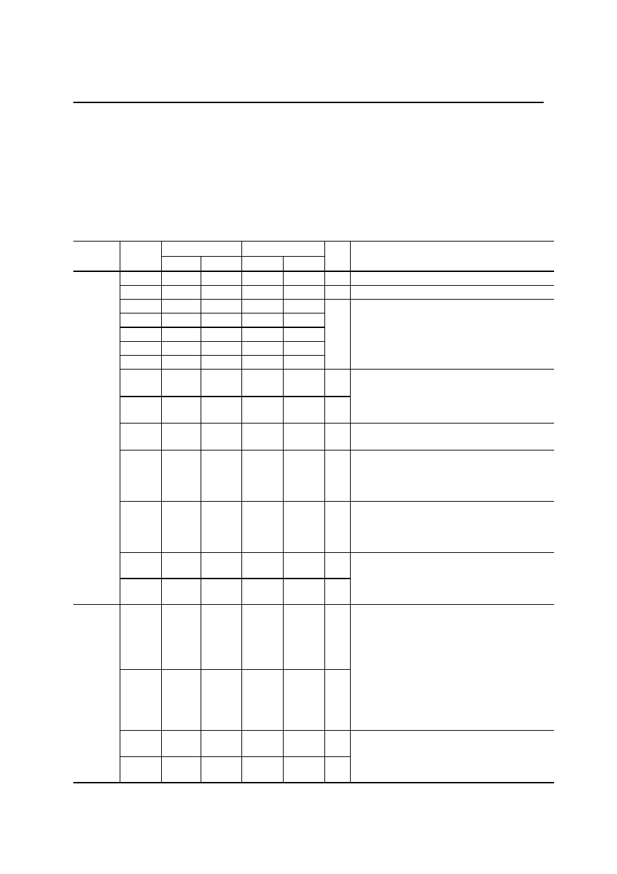
ABSOLUTE MAXIMUM RATINGS
(V
SS
= 0 V)
Parameter
Symbol
Condition
Rating
Unit
Power Supply Voltage 1
V
DD1
Ta = 25
∞
C
≠0.3 to +1.6
V
Power Supply Voltage 2
V
DD2
Ta = 25
∞
C
≠0.3 to +2.9
V
Power Supply Voltage 3
V
DD3
Ta = 25
∞
C
≠0.3 to +4.2
V
Power Supply Voltage 4
V
DD4
Ta = 25
∞
C
≠0.3 to +5.5
V
Power Supply Voltage 5
V
DD5
Ta = 25
∞
C
≠0.3 to +6.8
V
Power Supply Voltage 6
V
DD
Ta = 25
∞
C
≠0.3 to +6.0
V
Power Supply Voltage 7
V
DDI
Ta = 25
∞
C
≠0.3 to +6.0
V
Power Supply Voltage 8
V
DDH
Ta = 25
∞
C
≠0.3 to +6.0
V
Power Supply Voltage 9
V
DDL
Ta = 25
∞
C
≠0.3 to +6.0
V
Input Voltage 1
V
IN1
V
DD
Input, Ta = 25
∞
C
≠0.3 to V
DD
+0.3
V
Input Voltage 2
V
IN2
V
DDI
Input, Ta = 25
∞
C
≠0.3 to V
DDI
+0.3
V
Output Voltage 1
V
OUT1
V
DD1
Output, Ta = 25
∞
C
≠0.3 to V
DD1
+0.3
V
Output Voltage 2
V
OUT2
V
DD2
Output, Ta = 25
∞
C
≠0.3 to V
DD2
+0.3
V
Output Voltage 3
V
OUT3
V
DD3
Output, Ta = 25
∞
C
≠0.3 to V
DD3
+0.3
V
Output Voltage 4
V
OUT4
V
DD4
Output, Ta = 25
∞
C
≠0.3 to V
DD4
+0.3
V
Output Voltage 5
V
OUT5
V
DD5
Output, Ta = 25
∞
C
≠0.3 to V
DD5
+0.3
V
Output Voltage 6
V
OUT6
V
DD
Output, Ta = 25
∞
C
≠0.3 to V
DD
+0.3
V
Output Voltage 7
V
OUT7
V
DDI
Output, Ta = 25
∞
C
≠0.3 to V
DDI
+0.3
V
Output Voltage 8
V
OUT8
V
DDH
Output, Ta = 25
∞
C
≠0.3 to V
DDH
+0.3
V
Storage Temperature
T
STG
--
≠55 to +150
∞
C
FEDL63187B-06
1Semiconductor
ML63187B/63189B
19/36
RECOMMENDED OPERATING CONDITIONS
∑
When backup is used
(V
SS
= 0 V)
Parameter
Symbol
Condition
Range
Unit
Operating Temperature
T
op
--
≠20 to +70
∞
C
V
DD
--
0.9 to 2.7
V
Operating Voltage
V
DDI
--
0.9 to 5.5
V
Crystal Oscillation Frequency
f
XT
C
G
= 5 to 25 pF
32.768 to 76.8
kHz
R
OSL
= 1.0 M
36
±
30%
R
OSL
= 1.1 M
33
±
30%
Low-Speed RC Oscillation
Frequency
f
ROSL
R
OSL
= 1.2 M
30
±
30%
kHz
V
DD
= 0.9 to 1.2 V
Not applied
V
DD
= 1.2 to 2.7 V
300k to 500k
Ceramic Oscillation Frequency
f
CM
V
DD
= 1.5 to 2.7 V
200k to 1M
Hz
V
DD
= 0.9 to 1.2 V
Not applied
R
OSH
= 400 k
200k
±
30%
R
OSH
= 100 k
700k
±
30%
High-speed RC Oscillation
Frequency
f
ROSH
V
DD
= 1.2 to 2.7 V
R
OSH
= 75 k
1M
±
30%
Hz
∑
When backup is not used
(V
SS
= 0 V)
Parameter
Symbol
Condition
Range
Unit
Operating Temperature
T
op
--
≠20 to +70
∞
C
V
DD
--
1.8 to 5.5
Operating Voltage
V
DDI
--
1.8 to 5.5
V
Crystal Oscillation Frequency
f
XT
C
G
= 5 to 25 pF
32.768 to 76.8
kHz
R
OSL
= 1.0 M
36
±
30%
R
OSL
= 1.1 M
33
±
30%
Low-Speed RC Oscillation
Frequency
f
ROSL
R
OSL
= 1.2 M
30
±
30%
kHz
Ceramic Oscillation Frequency
f
CM
V
DD
= 1.8 to 5.5 V
200k to 2M
Hz
R
OSH
= 100 k
700k
±
30%
R
OSH
= 75 k
1M
±
30%
V
DD
= 1.8 to 5.5 V
R
OSH
= 51 k
1.35M
±
30%
High-speed RC Oscillation
Frequency
f
ROSH
V
DD
= 1.8 to 3.5 V, R
OSH
= 30 k
2M
±
30%
Hz

FEDL63187B-06
1Semiconductor
ML63187B/63189B
20/36
∑
Typical characteristics of low-speed RC oscillation
When backup is used/backup is not used (V
DD
= V
DDI
= 1.5 V/V
DD
= V
DDI
= 3.0 V)
∑
Typical characteristics of high-speed RC oscillation
When backup is used (V
DD
= V
DDI
= 1.5 V)
1000
100
10
100
1000
10000
f
RO
S
L
[
kH
z
]
R
OSL
[k
]
Reference data
10000
1000
100
10
100
1000
f
RO
S
H
[
kH
z
]
R
OSH
[k
]
Reference data
FEDL63187B-06
1Semiconductor
ML63187B/63189B
21/36
∑
Typical characteristics of high-speed RC oscillation
When backup is not used (V
DD
= V
DDI
= 3.0 V)
10000
1000
100
10
100
1000
f
RO
S
H
[
kH
z
]
R
OSH
[k
]
Reference data

FEDL63187B-06
1Semiconductor
ML63187B/63189B
22/36
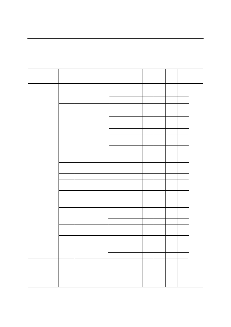
ELECTRICAL CHARACTERISTICS
DC Characteristics (1)
(V
DD
= V
DDI
= 0.9 to 5.5 V, V
SS
= 0 V, Ta = ≠20 to +70∞C unless otherwise specified)
Parameter
Symbol
Condition
Min.
Typ.
Max.
Unit
Mea-
suring
Circuit
V
DD2
Voltage
V
DD2
1/5 bias, 1/4 bias (Ta = 25∞C)
1.7
1.8
1.9
V
V
DD2
Voltage Temperature
Deviation
V
DD2
--
--
≠4
--
mV/∞C
V
DD1
Voltage
V
DD1
1/5 bias, 1/4 bias
Typ. ≠ 0.1
1/2
◊
V
DD2
Typ. + 0.1
V
1/5 bias
Typ. ≠ 0.3
3/2
◊
V
DD2
Typ. + 0.3
V
DD3
Voltage
V
DD3
1/4 bias (connect V
DD3
and V
DD2
)
Typ. ≠ 0.2
V
DD2
Typ. + 0.2
V
1/5 bias
Typ. ≠ 0.4
2
◊
V
DD2
Typ. + 0.4
V
DD4
Voltage
V
DD4
1/4 bias
Typ. ≠ 0.3
3/2
◊
V
DD2
Typ. + 0.3
V
1/5 bias
Typ. ≠ 0.5
5/2
◊
V
DD2
Typ. + 0.5
V
DD5
Voltage
V
DD5
1/4 bias
Typ. ≠ 0.4
2
◊
V
DD2
Typ. + 0.4
V
High-speed clock oscillation
stopped
V
DD
= 1.5 V
2.8
--
3.0
V
V
DDH
Voltage (Backup used)
V
DDH
High-speed clock oscillation
(Ceramic oscillation, 1 MHz)
V
DD
= 1.5 V
2.0
--
2.7
V
High-speed clock oscillation
stopped
1.0
1.5
2.0
V
V
DDL
Voltage
V
DDL
High-speed clock oscillation
(V
DD
= 1.2 to 5.5 V)
1.2
--
5.5
V
Crystal Oscillation Start
Voltage
V
STA
Oscillation start time:
within 5 seconds
1.2
--
--
V
Backup
0.9
--
--
V
Crystal Oscillation Hold
Voltage
V
HOLD
Backup not used
1.7
--
--
V
Crystal Oscillation Stop
Detect Time
T
STOP
--
0.1
--
5.0
ms
External Crystal Oscillator
Capacitance
C
G
--
5
--
25
pF
Internal Crystal Oscillator
Capacitance
C
D
--
20
25
30
pF
External Ceramic Oscillator
Capacitance
C
L0,1
CSA2.00MG
(Murata MFG.-make) used
V
DD
= 3.0 V
--
30
--
pF
Internal RC Oscillator
Capacitance
C
OS
--
8
12
16
pF
V
DD
= 1.5 V
0
--
0.4
V
POR Voltage
V
POR1
V
DD
= 3.0 V
0
--
0.7
V
V
DD
= 1.5 V
1.2
--
1.5
V
Non-POR Voltage
V
POR2
V
DD
= 3.0 V
2.0
--
3.0
V
1
LD1 = 1, LD0 = 1, Ta = 25∞C
2.30
2.40
2.50
LD1 = 1, LD0 = 0, Ta = 25∞C
1.70
1.80
1.90
LD1 = 0, LD0 = 1, Ta = 25∞C
1.10
1.20
1.30
BLD Judgment Voltage
V
BLDC
LD1 = 0, LD0 = 0, Ta = 25∞C
0.95
1.05
1.15
V
V
BLDC
= 2.40 V (LD1 = 1, LD0 = 1)
--
≠3.5
--
V
BLDC
= 1.80 V (LD1 = 1, LD0 = 0)
--
≠2.3
--
V
BLDC
= 1.20 V (LD1 = 0, LD0 = 1)
--
≠1.6
--
BLD Judgment Voltage
Temperature Deviation
V
BLDC
V
BLDC
= 1.05 V (LD1 = 0, LD0 = 0)
--
≠1.2
--
mV/∞C
--

FEDL63187B-06
1Semiconductor
ML63187B/63189B
23/36
Notes: 1. "T
STOP
" indicates that if the crystal oscillator stops over the value of T
STOP
, the system reset
occurs.
2. "POR" denotes Power On Reset.
3. "V
POR1
" indicates that POR occurs when V
DD
falls from V
DD
to V
POR1
and again rises up to V
DD
.
4. "V
POR2
" indicates that POR does not occur when V
DD
falls from V
DD
to V
POR2
and again rises up
to V
DD
.

FEDL63187B-06
1Semiconductor
ML63187B/63189B
24/36
DC Characteristics (2)
∑
When backup is used
(32.768 kHz crystal is used for the low-speed clock, V
DD
= V
DDI
= 1.5 V, V
SS
= 0 V, 1/5 bias,
LCD contrast (DSPCNT) = 0H, Ta = ≠20 to +70∞C unless otherwise specified)
Parameter
Symbol
Condition
Min.
Typ. Max.
Unit
Mea-
suring
Circuit
Ta = ≠20 to +50∞C
--
5
6.5
Supply Current 1
I
DD1
CPU is in HALT state.
(High-speed clock
oscillation stopped)
Ta = ≠20 to +70∞C
--
5
10
µ
A
Ta = ≠20 to +50∞C
--
4
5
Supply Current 2
I
DD2
CPU is in HALT state.
LCD is in Power Down
mood.
(High-speed clock
oscillation stopped)
Ta = ≠20 to +70∞C
--
4
8
µ
A
Ta = ≠20 to +50∞C
--
16
18
Supply Current 3
I
DD3
CPU is in operation at
low-speed oscillation.
(High-speed clock
oscillation stopped)
Ta = ≠20 to +70∞C
--
16
20
µ
A
Supply Current 4
I
DD4
CPU is in operation at high-speed oscillation
(approx. 700 kHz RC oscillation,
R
OSH
= 100 k
)
--
800
1000
µ
A
Supply Current 5
I
DD5
CPU is in operation at high-speed oscillation
(Ceramic oscillation, 1 MHz)
--
700
850
µ
A
1
∑
When backup is not used
(32.768 kHz crystal is used for the low-speed clock, V
DD
= V
DDI
= 3.0 V, V
SS
= 0 V, 1/5 bias,
LCD contrast (DSPCNT) = 0H, Ta = ≠20 to +70∞C unless otherwise specified)
Parameter
Symbol
Condition
Min.
Typ. Max.
Unit
Mea-
suring
Circuit
Ta = ≠20 to +50∞C
--
2.2
3
Supply Current 1
I
DD1
CPU is in HALT state.
(High-speed clock
oscillation stopped)
Ta = ≠20 to +70∞C
--
2.2
5
µ
A
Ta = ≠20 to +50∞C
--
1.8
2.5
Supply Current 2
I
DD2
CPU is in HALT state.
LCD is in Power Down
mood.
(High-speed clock
oscillation stopped)
Ta = ≠20 to +70∞C
--
1.8
4
µ
A
Ta = ≠20 to +50∞C
--
7.5
9
Supply Current 3
I
DD3
CPU is in operation at
low-speed oscillation.
(High-speed clock
oscillation stopped)
Ta = ≠20 to +70∞C
--
7.5
12
µ
A
Supply Current 4
I
DD4
CPU is in operation at high-speed oscillation
(approx. 700 kHz RC oscillation,
R
OSH
= 100 k
)
--
550
700
µ
A
Supply Current 5
I
DD5
CPU is in operation at high-speed oscillation
(Ceramic oscillation, 2 MHz)
--
850
1000
µ
A
1
FEDL63187B-06
1Semiconductor
ML63187B/63189B
25/36
DC Characteristics (3)
(V
DD
= V
DDI
= V
DDH
= 3.0 V, V
DD1
= 1.1 V, V
DD2
= 2.2 V, V
DD3
= 3.3 V, V
DD4
= 4.4 V,
V
DD5
= 5.5 V, Ta = ≠20 to +70∞C unless otherwise specified)
Parameter
Symbol
Condition
Min.
Typ.
Max.
Unit
Mea-
suring
Circuit
V
DDI
= 1.5 V
≠2.5
≠1.4
≠0.4
mA
V
DDI
= 3.0 V
≠6.0
≠3.5
≠1.0
mA
I
OH1
V
OH1
= V
DDI
≠ 0.5 V
V
DDI
= 5.0 V
≠8.5
≠5.0
≠1.5
mA
V
DDI
= 1.5 V
0.4
1.4
2.5
mA
V
DDI
= 3.0 V
1.0
3.0
6.0
mA
Output Current 1
(P9.0 to P9.3)*
(PA.0 to PA.3)*
(PB.0 to PB.3)
(PE.0 to PE.3)
I
OL1
V
OL1
= 0.5 V
V
DDI
= 5.0 V
1.5
3.7
8.5
mA
V
DD
= 1.5 V
≠4.0
≠2.0
≠0.5
mA
V
DD
= 3.0 V
≠11.0
≠6.0
≠2.0
mA
I
OH2
V
OH2
= V
DD
≠ 0.7 V
V
DD
= V
DDH
= 5.0 V
≠14.0
≠9.0
≠4.0
mA
V
DD
= 1.5 V
0.5
2.0
4.0
mA
V
DD
= 3.0 V
2.0
5.5
11.0
mA
Output Current 2
(MD, MDB)
I
OL2
V
OL2
= 0.7 V
V
DD
= V
DDH
= 5.0 V
4.0
7.0
14.0
mA
I
OH3
V
OH3
= V
DD5
≠ 0.2 V (V
DD5
Ievel)
--
--
≠4
µ
A
I
OHM3
V
OHM3
= V
DD4
+ 0.2 V (V
DD4
Ievel)
4
--
--
µ
A
I
OHM3S
V
OHM3S
= V
DD4
≠ 0.2 V (V
DD4
Ievel)
--
--
≠4
µ
A
I
OMH3
V
OMH3
= V
DD3
+ 0.2 V (V
DD3
Ievel)
4
--
--
µ
A
I
OMH3S
V
OMH3S
= V
DD3
≠ 0.2 V (V
DD3
Ievel)
--
--
≠4
µ
A
I
OML3
V
OML3
= V
DD2
+ 0.2 V (V
DD2
Ievel)
4
--
--
µ
A
I
OML3S
V
OML3S
= V
DD2
≠ 0.2 V (V
DD2
Ievel)
--
--
≠4
µ
A
I
OLM3
V
OLM3
= V
DD1
+ 0.2 V (V
DD1
Ievel)
4
--
--
µ
A
I
OLM3S
V
OLM3S
= V
DD1
≠ 0.2 V (V
DD1
Ievel)
--
--
≠4
µ
A
Output Current 3
(SEG0 to
SEG63)
(COM1 to
COM16)
I
OL3
V
OL3
= V
SS
+ 0.2 V (V
SS
Ievel)
4
--
--
µ
A
V
DD
= V
DDH
= 3.0 V
≠2.5
≠1.3
≠0.25
mA
I
OH4R
V
OH4R
= V
DDH
≠ 0.5 V
(RC oscillation)
V
DD
= V
DDH
= 5.0 V
≠3.5
≠1.7
≠0.5
mA
V
DD
= V
DDH
= 3.0 V
0.25
1.5
2.5
mA
I
OL4R
V
OL4R
= 0.5 V
(RC oscillation)
V
DD
= V
DDH
= 5.0 V
0.5
1.8
3.5
mA
V
DD
= V
DDH
= 3.0 V
≠500 ≠250 ≠100
µ
A
I
OH4C
V
OH4C
= V
DDH
≠ 0.5 V
(ceramic oscillation) V
DD
= V
DDH
= 5.0 V
≠800 ≠350 ≠200
µ
A
V
DD
= V
DDH
= 3.0 V
200
500
800
µ
A
Output Current 4
(OSC1)
I
OL4C
V
OL4C
= 0.5 V
(ceramic oscillation) V
DD
= V
DDH
= 5.0 V
400
700
1000
µ
A
I
OOH
V
OH
= V
DDI
--
--
0.3
µ
A
Output Leakage
Current
(P9.0 to P9.3)*
(PA.0 to PA.3)*
(PB.0 to PB.3)
(PE.0 to PE.3)
I
OOL
V
OL
= V
SS
≠0.3
--
--
µ
A
2
*: Applied to the ML63189B only.

FEDL63187B-06
1Semiconductor
ML63187B/63189B
26/36
DC Characteristics (4)
(V
DD
= V
DDI
= V
DDH
= 3.0 V, V
DD1
= 1.1 V, V
DD2
= 2.2 V, V
DD3
= 3.3 V, V
DD4
= 4.4 V,
V
DD5
= 5.5 V, Ta = ≠20 to +70∞C unless otherwise specified)
Parameter
Symbol
Condition
Min.
Typ.
Max.
Unit
Mea-
suring
Circuit
V
DDI
= 1.5 V
2
20
45
µ
A
V
DDI
= 3.0 V
30
120
260
µ
A
I
IH1
V
OH1
= V
DDI
(when pulled up)
V
DDI
= 5.0 V
70
350
650
µ
A
V
DDI
= 1.5 V
≠45
≠20
≠2
µ
A
V
DDI
= 3.0 V
≠260
≠120
≠30
µ
A
I
IL1
V
IL1
= V
SS
(when pulled up)
V
DDI
= 5.0 V
≠650
≠350
≠70
µ
A
I
IH1Z
V
IH1
= V
DDI
(in a high impedance state)
0
--
1
µ
A
Input Current 1
(P0.0 to P0.3)*
(P9.0 to P9.3)*
(PA.0 to PA.3)*
(PB.0 to PB.3)
(PE.0 to PE.3)
I
IL1Z
V
IL1
= V
SS
(in a high impedance state)
≠1
--
0
µ
A
V
DD
= V
DDH
= 3.0 V
≠350
≠170
≠30
µ
A
I
IL2
V
IL2
= V
SS
(when pulled up)
V
DD
= V
DDH
= 5.0 V
≠750
≠450 ≠200
µ
A
I
IH2R
V
IH2R
= V
DDH
(RC oscillation)
0
--
1
µ
A
I
IL2R
V
IL2R
= V
SS
(RC oscillation)
≠1
--
0
µ
A
V
DD
= V
DDH
= 3.0 V
0.5
1.8
4.0
µ
A
I
IH2C
V
IH2C
= V
DDH
(ceramic oscillation)
V
DD
= V
DDH
= 5.0 V
3
6
10
µ
A
V
DD
= V
DDH
= 3.0 V
≠4.0
≠1.8
≠0.5
µ
A
Input Current 2
(OSC0)
I
IL2C
V
IL2C
= V
SS
(ceramic oscillation)
V
DD
= V
DDH
= 5.0 V
≠10
≠6
≠3
µ
A
V
DD
= 1.5 V
10
180
350
µ
A
V
DD
= 3.0 V
150
1100 2400
µ
A
I
IH3
V
IH3
= V
DD
V
DD
= V
DDH
= 5.0 V
0.5
2.7
5.0
mA
Input Current 3
(RESET)
I
IL3
V
IL3
= V
SS
≠1
--
0
µ
A
V
DD
= 1.5 V
50
750
1500
µ
A
V
DD
= 3.0 V
0.5
3.0
5.5
mA
I
IH4
V
IH4
= V
DD
V
DD
= V
DDH
= 5.0 V
2.0
6.5
11.0
mA
Input Current 4
(TST1, TST2)
I
IL4
V
IL4
= V
SS
≠1
--
0
µ
A
3
*: Applied to the ML63189B only.

FEDL63187B-06
1Semiconductor
ML63187B/63189B
27/36
DC Characteristics (5)
(V
DD
= V
DDI
= V
DDH
= 3.0 V, V
DD1
= 1.1 V, V
DD2
= 2.2 V, V
DD3
= 3.3 V, V
DD4
= 4.4 V,
V
DD5
= 5.5 V, Ta = ≠20 to +70∞C unless otherwise specified)
Parameter
Symbol
Condition
Min.
Typ.
Max.
Unit
Measuring
Circuit
V
DDI
= 1.5 V
1.2
--
1.5
V
V
DDI
= 3.0 V
2.4
--
3.0
V
V
IH1
V
DDI
= 5.0 V
4.0
--
5.0
V
V
DDI
= 1.5 V
0
--
0.3
V
V
DDI
= 3.0 V
0
--
0.6
V
Input Voltage 1
(P0.0 to P0.3)*
(P9.0 to P9.3)*
(PA.0 to PA.3)*
(PB.0 to PB.3)
(PE.0 to PE.3)
V
IL1
V
DDI
= 5.0 V
0
--
1.0
V
V
DD
= V
DDH
= 3.0 V
2.4
--
3.0
V
V
IH2
V
DD
= V
DDH
= 5.0 V
4.0
--
5.0
V
V
DD
= V
DDH
= 3.0 V
0
--
0.6
V
Input Voltage 2
(OSC0)
V
IL2
V
DD
= V
DDH
= 5.0 V
0
--
1.0
V
V
DD
= 1.5 V
1.35
--
1.5
V
V
DD
= 3.0 V
2.4
--
3.0
V
V
IH3
V
DD
= 5.0 V
4.0
--
5.0
V
V
DD
= 1.5 V
0
--
0.15
V
V
DD
= 3.0 V
0
--
0.6
V
Input Voltage 3
(RESET, TST1, TST2)
V
IL3
V
DD
= 5.0 V
0
--
1.0
V
V
DDI
= 1.5 V
0.05
0.1
0.3
V
V
DDI
= 3.0 V
0.2
0.5
1.0
V
Hysteresis Width 1
(P0.0 to P0.3)*
(P9.0 to P9.3)*
(PA.0 to PA.3)*
(PB.0 to PB.3)
(PE.0 to PE.3)
V
T1
V
DDI
= 5.0 V
0.25
1.0
1.5
V
V
DDI
= 1.5 V
0.05
0.1
0.3
V
V
DDI
= 3.0 V
0.2
0.5
1.0
V
Hysteresis Width 2
(RESET, TST1, TST2)
V
T2
V
DDI
= 5.0 V
0.25
1.0
1.5
V
4
Input Pin Capacitance
(P0.0 to P0.3)*
(P9.0 to P9.3)*
(PA.0 to PA.3)*
(PB.0 to PB.3)
(PE.0 to PE.3)
C
IN
--
--
--
5
pF
1
*: Applied to the ML63189B only.

FEDL63187B-06
1Semiconductor
ML63187B/63189B
28/36
Measuring circuit 1
C
a
,C
b
,C
c
,C
d
,C
e
,C
l
,C
12
C
h
,Cb
12
C
G
C
L0
C
L1
Ceramic Resonator
V
V
Ca
Cc
V
DD3
V
DD1
V
DDI
V
SS
XT0
XT1
*1 RC Oscillator
R
OSH
Ceramic Oscillator
C
L0
:
:
:
:
:
:
0.1 µF
1 µF
15 pF
30 pF
30 pF
CSA2.00MG (2 MHz)
CSB1000J (1 MHz)
(Murata MFG-.make)
Cb12
CB1
CB2
OSC0
OSC1
A
V
DD
V
Cd
V
DD4
C
L1
Ceramic Resonator
*1
C12
C1
C2
V
Cb
V
DD2
Ce
V
DD5
V
V
Ch
V
DDH
Cl
V
DDL
V
*2
*2 RC Oscillator
R
OSL
Crystal Oscillator
C
G
Crystal
1
2
3
4
1
2
1
2
3
4
3
4

FEDL63187B-06
1Semiconductor
ML63187B/63189B
29/36
Measuring circuit 2
Measuring circuit 3
Measuring circuit 4
V
SS
A
V
IH
V
lL
*2
V
DD
V
DDl
V
DD1
V
DD2
V
DD3
V
DD4
V
DD5
V
DDH
INPUT
OUTPUT
*3
V
DDL
*2 Input logic circuit to determine the specified measuring conditions.
*3 Measured at the specified output pins.
V
SS
V
DD
V
DDl
V
DD1
V
DD2
V
DD3
V
DD4
V
DD5
V
DDH
INPUT
OUTPUT
A
*4
V
DDL
V
SS
V
IH
V
IL
*4
V
DD
V
DDl
V
DD1
V
DD2
V
DD3
V
DD4
V
DD5
V
DDH
INPUT
OUTPUT
*4 Measured at the specified input pins.
Waveform
Monitoring
V
DDL

FEDL63187B-06
1Semiconductor
ML63187B/63189B
30/36
AC Characteristics (Serial Interface, Shift Register)
(V
DD
= 0.9 to 5.5 V, V
DDH
= 1.8 to 5.5 V, V
SS
= 0 V, V
DDI
= 5.0 V, Ta = ≠20 to +70
∞
C unless otherwise specified)
Parameter
Symbol
Condition
Min.
Typ.
Max.
Unit
SCLK Input Fall Time
t
f
--
--
--
1.0
µ
s
SCLK Input Rise Time
t
r
--
--
--
1.0
µ
s
SCLK Input "L" Level
Pulse Width
t
CWL
--
0.8
--
--
µ
s
SCLK Input "H" Level
Pulse Width
t
CWH
--
0.8
--
--
µ
s
SCLK Input Cycle Time
t
CYC
V
DDI
= 5 V to V
DD
1.8
--
--
µ
s
t
CYC1(O)
CPU in operation state at 32.768 kHz
--
30.5
--
µ
s
SCLK Output Cycle Time
t
CYC2(O)
CPU in operation at 2 MHz
V
DD
= V
DDH
= 1.8 to 3.5 V
--
0.5
--
µ
s
SOUT Output Delay Time
t
DDR
Output load capacitance 10 pF
--
--
0.4
µ
s
SIN Input Setup Time
t
DS
--
0.5
--
--
µ
s
SIN Input Hold Time
t
DH
--
0.8
--
--
µ
s
AC characteristics timing
("H" level = 4.0 V, "L" level = 1.0 V)
t
CYC
SOUT (PE.1)
SIN (PE.0)
t
DDR
t
r
t
f
t
CWH
t
CWL
t
DDR
t
DS
t
DS
t
DH
5 V (V
DDl
)
0 V (V
SS
)
5 V (V
DDI
)
0 V (V
SS
)
5 V (V
DDI
)
0 V (V
SS
)
SCLK (PE.2)

FEDL63187B-06
1Semiconductor
ML63187B/63189B
31/36
APPLICATION CIRCUITS (ML63187B)
Note:
V
DDI
is the power supply pin for the input-output ports.
Be sure to connect the V
DDI
pin either to the positive power supply pin (V
DD
) of this device
or to the positive power supply pin of the external memory.
Application Circuit Example with Power Supply Backup
XT0
COM1-16
XT1
V
DDH
V
DD
CB1
CB2
V
DD5
V
DD4
V
DD3
V
DD2
V
DD1
C1
C2
RESET
TST1
TST2
MD
MDB
V
SS
SEG0-63
OSC0
OSC1
R
OSH
PB.3
PB.2
PB.1
PB.0
C
b12
C
v
C
G
C
12
LCD
Crystal
32.768 kHz
C
h
1.5 V
C
e
C
d
C
c
C
b
C
a
Buzzer
∑
Crystal oscillation is selected as low-speed
oscillation by mask option.
∑
RC oscillation is selected as high-speed
oscillation by software.
∑
Ports are powered from external memory
power source.
∑
C
V
is an IC power supply bypass capacitor.
∑
Values of C
a
, C
b
, C
c
, C
d
, C
e
, C
l
, C
b12
, C
12
,
C
h
, and C
G
, are for reference only.
V
DDl
V
DDL
C
l
Push SW
0.1
µ
F
0.1
µ
F
0.1
µ
F
0.1
µ
F
0.1
µ
F
0.1
µ
F
1.0
µ
F
0.1
µ
F
1.0
µ
F
5 to
25 pF
ML63187B
PE.3
PE.2
PE.1
PE.0
V
DD
1.0
µ
F

FEDL63187B-06
1Semiconductor
ML63187B/63189B
32/36
Note:
V
DDI
is the power supply pin for the input-output ports.
Be sure to connect the V
DDI
pin either to the positive power supply pin (V
DD
) of this device
or to the positive power supply pin of the external memory.
Application Circuit Example with No Power Supply Backup
XT0
COM1-16
XT1
V
DDH
V
DD
V
DD5
V
DD4
V
DD3
V
DD2
V
DD1
C1
C2
RESET
TST1
TST2
MD
MDB
V
SS
SEG0-63
OSC0
OSC1
PB.3
PB.2
PB.1
PB.0
C
v
C
G
C
12
LCD
Crystal
32.768 kHz
V
DD
5.0 V
C
e
C
d
C
c
C
v
C
a
Buzzer
∑
Crystal oscillation is selected as low-speed
oscillation by mask option.
∑
Ceramic oscillation is selected as high-speed
oscillation by software.
∑
Ports, external memory, and IC share their
power supply.
∑
C
v
is an IC power supply bypass capacitor.
∑
Values of C
a
, C
b
, C
c
, C
d
, C
e
, C
l
, C
12
, C
G
,
C
L0
, and C
L1
are for reference only.
V
DDl
V
DD
C
L0
30 pF
C
L1
30 pF
Ceramic
Resonator
(Example: 1 MHz)
CB1
CB2
V
DDL
C
l
ML63187B
0.1
µ
F
0.1
µ
F
0.1
µ
F
0.1
µ
F
0.1
µ
F
0.1
µ
F
0.1
µ
F
Open
Push SW
5 to 25 pF
PE.3
PE.2
PE.1
PE.0
0.1
µ
F
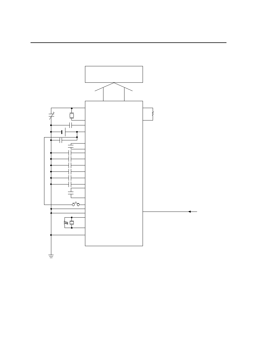
FEDL63187B-06
1Semiconductor
ML63187B/63189B
33/36
APPLICATION CIRCUITS (ML63189B)
Note:
V
DDI
is the power supply pin for the input and input-output ports.
Be sure to connect the V
DDI
pin either to the positive power supply pin (V
DD
) of this device
or to the positive power supply pin of the external memory.
Application Circuit Example with Power Supply Backup
XT0
COM1-16
XT1
V
DDH
V
DD
CB1
CB2
V
DD5
V
DD4
V
DD3
V
DD2
V
DD1
C1
C2
RESET
TST1
TST2
MD
MDB
V
SS
SEG0-63
OSC0
OSC1
R
OSH
P9.3
P9.2
P9.1
P9.0
PB.3
PB.2
PB.1
PB.0
PA.3
PA.2
PA.1
PA.0
C
b12
C
v
C
G
C
12
LCD
Crystal
32.768 kHz
C
h
1.5 V
C
e
C
d
C
c
C
b
C
a
Buzzer
∑
Crystal oscillation is selected as low-speed
oscillation by mask option.
∑
RC oscillation is selected as high-speed
oscillation by software.
∑
Ports are powered from external memory
power source.
∑
C
v
is an IC power supply bypass capacitor.
∑
Values of C
a
, C
b
, C
c
, C
d
, C
e
, C
l
, C
b12
, C
12
,
C
h
, and C
G
, are for reference only.
V
DDI
V
DDL
C
l
Push SW
0.1
µ
F
0.1
µ
F
0.1
µ
F
0.1
µ
F
0.1
µ
F
0.1
µ
F
1.0
µ
F
0.1
µ
F
1.0
µ
F
5 to
25 pF
ML63189B
PE.3
PE.2
PE.1
PE.0
P0.3
P0.2
P0.1
P0.0
V
DD
1.0
µ
F

FEDL63187B-06
1Semiconductor
ML63187B/63189B
34/36
Note:
V
DDI
is the power supply pin for the input and input-output ports.
Be sure to connect the V
DDI
pin either to the positive power supply pin (V
DD
) of this device
or to the positive power supply pin of the external memory.
Application Circuit Example with No Power Supply Backup
XT0
COM1-16
XT1
V
DDH
V
DD
V
DD5
V
DD4
V
DD3
V
DD2
V
DD1
C1
C2
RESET
TST1
TST2
MD
MDB
V
SS
SEG0-63
OSC0
OSC1
P9.3
P9.2
P9.1
P9.0
PB.3
PB.2
PB.1
PB.0
PA.3
PA.2
PA.1
PA.0
C
v
C
G
C
12
LCD
Crystal
32.768 kHz
V
DD
5.0 V
C
e
C
d
C
c
C
b
C
a
Buzzer
∑
Crystal oscillation is selected as low-speed
oscillation by mask option.
∑
Ceramic oscillation is selected as high-speed
oscillation by software.
∑
Ports, external memory, and IC share their
power supply.
∑
C
v
is an IC power supply bypass capacitor.
∑
Values of C
a
, C
b
, C
c
, C
d
, C
e
, C
l
, C
12
, C
G
,
C
L0
, and C
L1
are for reference only.
V
DDl
V
DD
C
L0
30 pF
C
L1
30 pF
Ceramic
Resonator
(Example: 1 MHz)
CB1
CB2
V
DDL
C
l
ML63189B
0.1
µ
F
0.1
µ
F
0.1
µ
F
0.1
µ
F
0.1
µ
F
0.1
µ
F
0.1
µ
F
Open
Push SW
5 to 25 pF
PE.3
PE.2
PE.1
PE.0
P0.3
P0.2
P0.1
P0.0
0.1
µ
F

FEDL63187B-06
1Semiconductor
ML63187B/63189B
35/36
PACKAGE DIMENSIONS
Notes for Mounting the Surface Mount Type Package
The surface mount type packages are very susceptible to heat in reflow mounting and humidity
absorbed in storage.
Therefore, before you perform reflow mounting, contact Oki's responsible sales person for the product
name, package name, pin number, package code and desired mounting conditions (reflow method,
temperature and times).
QFP128-P-1420-0.50-K
Mirror finish
Package material
Epoxy resin
Lead frame material
42 alloy
Pin treatment
Solder plating (
5µm)
Package weight (g)
1.19 TYP.
5
Rev. No./Last Revised
4/Nov. 28, 1996
(Unit: mm)

FEDL63187B-06
1Semiconductor
ML63187B/63189B
36/36
NOTICE
1.
The information contained herein can change without notice owing to product and/or technical improvements.
Before using the product, please make sure that the information being referred to is up-to-date.
2.
The outline of action and examples for application circuits described herein have been chosen as an
explanation for the standard action and performance of the product. When planning to use the product, please
ensure that the external conditions are reflected in the actual circuit, assembly, and program designs.
3.
When designing your product, please use our product below the specified maximum ratings and within the
specified operating ranges including, but not limited to, operating voltage, power dissipation, and operating
temperature.
4.
Oki assumes no responsibility or liability whatsoever for any failure or unusual or unexpected operation
resulting from misuse, neglect, improper installation, repair, alteration or accident, improper handling, or
unusual physical or electrical stress including, but not limited to, exposure to parameters beyond the specified
maximum ratings or operation outside the specified operating range.
5.
Neither indemnity against nor license of a third party's industrial and intellectual property right, etc. is
granted by us in connection with the use of the product and/or the information and drawings contained herein.
No responsibility is assumed by us for any infringement of a third party's right which may result from the use
thereof.
6.
The products listed in this document are intended for use in general electronics equipment for commercial
applications (e.g., office automation, communication equipment, measurement equipment, consumer
electronics, etc.). These products are not authorized for use in any system or application that requires special
or enhanced quality and reliability characteristics nor in any system or application where the failure of such
system or application may result in the loss or damage of property, or death or injury to humans.
Such applications include, but are not limited to, traffic and automotive equipment, safety devices, aerospace
equipment, nuclear power control, medical equipment, and life-support systems.
7.
Certain products in this document may need government approval before they can be exported to particular
countries. The purchaser assumes the responsibility of determining the legality of export of these products
and will take appropriate and necessary steps at their own expense for these.
8.
No part of the contents contained herein may be reprinted or reproduced without our prior permission.
Copyright 2001 Oki Electric Industry Co., Ltd
.