
ML63187/189B/193
User's Manual
NOTICE: ML63187 is replaced by ML63189B. Order stop for new masks for ML63187
FIRST EDITION
ISSUE DATE: Mar. 2000
FEUL63193-01
°

NOTICE
1.
The information contained herein can change without notice owing to product and/or
technical improvements. Before using the product, please make sure that the information
being referred to is up-to-date.
2.
The outline of action and examples for application circuits described herein have been
chosen as an explanation for the standard action and performance of the product. When
planning to use the product, please ensure that the external conditions are reflected in the
actual circuit, assembly, and program designs.
3.
When designing your product, please use our product below the specified maximum
ratings and within the specified operating ranges including, but not limited to, operating
voltage, power dissipation, and operating temperature.
4.
Oki assumes no responsibility or liability whatsoever for any failure or unusual or
unexpected operation resulting from misuse, neglect, improper installation, repair, alteration
or accident, improper handling, or unusual physical or electrical stress including, but not
limited to, exposure to parameters beyond the specified maximum ratings or operation
outside the specified operating range.
5.
Neither indemnity against nor license of a third party's industrial and intellectual property
right, etc. is granted by us in connection with the use of the product and/or the information
and drawings contained herein. No responsibility is assumed by us for any infringement
of a third party's right which may result from the use thereof.
6.
The products listed in this document are intended for use in general electronics equipment
for commercial applications (e.g., office automation, communication equipment,
measurement equipment, consumer electronics, etc.). These products are not authorized
for use in any system or application that requires special or enhanced quality and reliability
characteristics nor in any system or application where the failure of such system or
application may result in the loss or damage of property, or death or injury to humans.
Such applications include, but are not limited to, traffic and automotive equipment, safety
devices, aerospace equipment, nuclear power control, medical equipment, and life-support
systems.
7.
Certain products in this document may need government approval before they can be
exported to particular countries. The purchaser assumes the responsibility of determining
the legality of export of these products and will take appropriate and necessary steps at their
own expense for these.
8.
No part of the contents contained herein may be reprinted or reproduced without our prior
permission.
9.
MS-DOS is a registered trademark of Microsoft Corporation.
Copyright 2000 Oki Electric Industry Co., Ltd.
Printed in Japan
E2Y0002-2X-13


Preface
This manual describes the hardware of Oki's original CMOS 4-bit microcontrollers ML63187,
ML63189B, and ML63193.
Refer to the "nX-4/250 Core Instruction Manual" for details of the 4-bit CPU core nX-4/250
which is built in the ML63187, ML63189B, and ML63193.
The manuals related to the ML63187, ML63189B, and ML63193 are shown below.
∑ nX-4/250 Core Instruction Manual:
Describes the base architecture and instruction set of nX-4/250 core.
∑ SASM63K User's Manual:
Describes the structured assembler operation and assembler language specifica-
tion.
∑ EASE63180 User's Manual:
Describes the hardware of the emulator.
∑ DT63K Debugger/DTS63K Simulator User's Manual:
Describes the debugger commands and the hardware of the simulator.
This document is subject to change without notice.

Notation
Classification
Notation
Description
n Numeric value
xxh, xxH
Represents a hexadecimal number.
xxb
Represents a binary number.
n Unit
word, W
1 word = 16 bits
byte, B
1 byte = 2 nibbles = 8 bits
nibble, N
1 nibble = 4 bits
mega-, M
10
6
kilo-, K
2
10
= 1024
kilo-, k
10
3
= 1000
milli-, m
10
-3
micro-,
m
10
-6
nano-, n
10
-9
second, s (lower case)
second
KB
1 KB = 1 kilobyte = 1024 bytes
MB
1 MB = 1 megabyte = 2
20
bytes
= 1,048,576 bytes
n Symbol
Note:
Gives more information about mistakable items.
A chapter or page with this symbol describes the ML63187.
A chapter or page with this symbol describes the ML63189B.
A chapter or page with this symbol describes the ML63193.
n Terminology
"H" level
Indicates high side voltage signal levels V
IH
and
V
OH
as specified by the electrical characteristics.
"L" level
Indicates low side voltage signal levels V
IL
and
V
OL
as specified by the electrical characteristics.
n Register description
Invalid bit
:
When read, a value of "1" is always obtained. Write operations are invalid.
R/W attribute
:
"R" indicates data can be read and "W" indicates data can be written.
!
M187
M189B
Bit name
Invalid bit
Address
R/W attribute
Register name
PBF
--
PB1MOD
PB0MOD
bit 3
bit 2
bit 1
bit 0
PBMOD0
(032H)
(R/W)
M193

- i -
Table of Contents
Chapter 1 Overview
1.1 Overview ........................................................................................................ 1-1
1.2 Features ......................................................................................................... 1-1
1.3 Function List .................................................................................................. 1-5
1.4 Block Diagram ................................................................................................ 1-6
1.5 Pin Configuration ........................................................................................... 1-9
1.5.1 ML63187 Pin Configuration ................................................................ 1-9
1.5.2 ML63189B Pin Configuration .............................................................. 1-13
1.5.3 ML63193 Pin Configuration ................................................................ 1-17
1.6 Pin Descriptions ............................................................................................. 1-21
1.6.1 Descriptions of the Basic Functions of Each Pin ................................ 1-21
1.6.2 Descriptions of the Secondary Functions of Each Pin ........................ 1-26
1.6.3 Handling of Unused Pins .................................................................... 1-28
1.7 Basic Timing .................................................................................................. 1-29
1.7.1 Basic Timing of CPU Operation .......................................................... 1-29
1.7.2 Port I/O Basic Timing .......................................................................... 1-29
1.7.3 Interrupt Basic Timing ......................................................................... 1-31
Chapter 2 CPU and Memory Spaces
2.1 Overview ........................................................................................................ 2-1
2.2 Registers ........................................................................................................ 2-1
2.2.1 Accumulator (A) .................................................................................. 2-1
2.2.2 Flag Register ...................................................................................... 2-1
2.2.2.1 Carry Flag (C) ....................................................................... 2-1
2.2.2.2 Zero Flag (Z) ......................................................................... 2-2
2.2.2.3 G Flag (G) ............................................................................. 2-2
2.2.3 Master Interrupt Enable Flag (MIE) .................................................... 2-2
2.2.4 Current Bank Register (CBR), Extra Bank Register (EBR),
HL Register (HL), XY Register (XY) ................................................... 2-3
2.2.5 Program Counter (PC) ........................................................................ 2-4
2.2.6 RA Registers (RA3, RA2, RA1, RA0) ................................................. 2-4
2.2.7 Stack Pointer (SP) and Call Stack ...................................................... 2-5
2.2.8 Register Stack Pointer (RSP) and Register Stack .............................. 2-6
2.3 Memory Spaces ............................................................................................. 2-7
2.3.1 Program Memory Space ..................................................................... 2-7
2.3.2 Data Memory Space ........................................................................... 2-8

- ii -
Chapter 3 CPU Control Functions
3.1 Overview ........................................................................................................ 3-1
3.2 System Reset Mode (RST) ............................................................................ 3-2
3.2.1 Transfer to and State of System Reset Mode .................................... 3-2
3.3 Halt Mode ....................................................................................................... 3-4
3.3.1 Transfer to and State of Halt Mode .................................................... 3-4
3.3.2 Halt Mode Release ............................................................................. 3-5
3.3.2.1 Release of Halt Mode by Interrupt ........................................ 3-5
3.3.2.2 Release of Halt Mode by RESET Pin ................................... 3-5
3.3.3 Melody Data Interrupt and Halt Mode Release .................................. 3-6
3.3.4 Note Concerning HALT Instruction ..................................................... 3-6
Chapter 4 ML63187 Interrupt (INT187)
4.1 Overview ........................................................................................................ 4-1
4.2 Interrupt Registers ......................................................................................... 4-3
4.3 Interrupt Sequence ........................................................................................ 4-9
4.3.1 Interrupt Processing ........................................................................... 4-9
4.3.2 Return from an Interrupt Routine ........................................................ 4-10
4.3.3 Interrupt Hold Instructions .................................................................. 4-10
Chapter 5 ML63189B Interrupt (INT189)
5.1 Overview ........................................................................................................ 5-1
5.2 Interrupt Registers ......................................................................................... 5-3
5.3 Interrupt Sequence ........................................................................................ 5-9
5.3.1 Interrupt Processing ........................................................................... 5-9
5.3.2 Return from an Interrupt Routine ........................................................ 5-10
5.3.3 Interrupt Hold Instructions .................................................................. 5-10
Chapter 6 ML63193 Interrupt (INT193)
6.1 Overview ........................................................................................................ 6-1
6.2 Interrupt Registers ......................................................................................... 6-3
6.3 Interrupt Sequence ........................................................................................ 6-11
6.3.1 Interrupt Processing ........................................................................... 6-11
6.3.2 Return from an Interrupt Routine ........................................................ 6-12
6.3.3 Interrupt Hold Instructions .................................................................. 6-12
Chapter 7 Clock Generator Circuit (OSC)
7.1 Overview ........................................................................................................ 7-1
7.2 Clock Generator Circuit Configuration ........................................................... 7-1
7.3 Low-Speed Clock Generator Circuit .............................................................. 7-2
7.4 High-Speed Clock Generator Circuit .............................................................. 7-4
7.5 System Clock Control .................................................................................... 7-6
7.6 Frequency Control Register (FCON) ............................................................. 7-7
7.7 System Clock Select Timing .......................................................................... 7-8

- iii -
Chapter 8 Time Base Counter (TBC)
8.1 Overview ........................................................................................................ 8-1
8.2 Time Base Counter Configuration.................................................................. 8-1
8.3 Time Base Counter Registers ........................................................................ 8-2
8.4 Time Base Counter Operation ....................................................................... 8-2
Chapter 9 Timers (TIMER)
9.1 Overview ........................................................................................................ 9-1
9.2 Timer Configuration ....................................................................................... 9-1
9.3 Timer Registers .............................................................................................. 9-3
9.4 Timer Operation ............................................................................................. 9-14
9.4.1 Timer Clock ........................................................................................ 9-14
9.4.2 Timer Data Registers .......................................................................... 9-14
9.4.3 Timer Counter Registers .................................................................... 9-14
9.4.4 Timer Interrupt Requests and Overflow Flags .................................... 9-15
9.4.5 Auto-Reload Mode Operation ............................................................. 9-16
9.4.6 Capture Mode Operation .................................................................... 9-18
9.4.7 Frequency Measurement Mode Operation ......................................... 9-21
Chapter 10 100 Hz Timer Counter (100HzTC)
10.1 Overview ........................................................................................................ 10-1
10.2 100 Hz Timer Counter Configuration ............................................................. 10-1
10.3 100 Hz Timer Counter Registers ................................................................... 10-2
10.4 100 Hz Timer Counter Operation ................................................................... 10-3
Chapter 11 Watchdog Timer (WDT)
11.1 Overview ........................................................................................................ 11-1
11.2 Watchdog Timer Configuration ...................................................................... 11-1
11.3 Watchdog Timer Control Register (WDTCON) .............................................. 11-2
11.4 Watchdog Timer Operation ............................................................................ 11-2

- iv -
Chapter 12 Ports (INPUT, I/O PORT)
12.1 Overview ........................................................................................................ 12-1
12.2 Ports List ........................................................................................................ 12-1
12.3 Port 0 (P0.0≠P0.3) ......................................................................................... 12-2
12.3.1 Port 0 Configuration .......................................................................... 12-2
12.3.2 Port 0 Registers ................................................................................ 12-2
12.3.3 Port 0 External Interrupt Function (External Interrupt 5) ................... 12-5
12.4 Port 9, Port A (P9.0≠P9.3, PA.0≠PA.3) ......................................................... 12-7
12.4.1 Port 9, Port A Configuration .............................................................. 12-7
12.4.2 Port 9, Port A Registers .................................................................... 12-8
12.5 Port B (PB.0≠PB.3) ........................................................................................ 12-12
12.5.1 Port B Configuration ......................................................................... 12-12
12.5.2 Port B Registers ............................................................................... 12-13
12.5.3 Port B External Interrupt Function (External Interrupt 0) .................. 12-17
12.6 Port C (PC.0≠PC.3) ....................................................................................... 12-18
12.6.1 Port C Configuration ......................................................................... 12-18
12.6.2 Port C Registers ............................................................................... 12-19
12.6.3 Port C External Interrupt Function (External Interrupt 1) .................. 12-24
12.7 Port E (PE.0≠PE.3) ........................................................................................ 12-25
12.7.1 Port E Configuration ......................................................................... 12-25
12.7.2 Port E Registers ............................................................................... 12-26
12.7.3 Port E.3 External Interrupt Function (External Interrupt 2) ............... 12-29
Chapter 13 Melody Driver (MELODY)
13.1 Overview ........................................................................................................ 13-1
13.2 Melody Driver Configuration .......................................................................... 13-1
13.3 Melody Driver Registers ................................................................................. 13-2
13.4 Melody Circuit Operation ............................................................................... 13-4
13.4.1 Tempo Data ...................................................................................... 13-5
13.4.2 Melody Data ..................................................................................... 13-6
13.4.3 Melody Circuit Application Example ................................................. 13-9
13.5 Buzzer Circuit Operation ................................................................................ 13-10
Chapter 14 Serial Port (SIO)
14.1 Overview ........................................................................................................ 14-1
14.2 Serial Port Configuration ................................................................................ 14-1
14.3 Serial Port Registers ...................................................................................... 14-3
14.4 Serial Port Operation Description .................................................................. 14-12
14.4.1 Data Format ...................................................................................... 14-12
14.4.2 Send Operation Description ............................................................. 14-13
14.4.3 Receive Operation Description ......................................................... 14-19
14.5 Send/Receive Data LSB/MSB First Select .................................................... 14-25
14.5.1 Selecting Send Data LSB/MSB First ................................................ 14-25
14.5.2 Selecting Receive Data LSB/MSB First ............................................ 14-26

- v -
Chapter 15 Shift Register (SFT)
15.1 Overview ........................................................................................................ 15-1
15.2 Shift Register Configuration ........................................................................... 15-1
15.3 Shift Registers ................................................................................................ 15-2
15.4 Shift Register Operation ................................................................................ 15-4
15.5 Shift Register Application Example ................................................................ 15-6
Chapter 16 LCD Driver (LCD)
16.1 Overview ........................................................................................................ 16-1
16.2 LCD Driver Configuration ............................................................................... 16-1
16.3 LCD Driver Registers ..................................................................................... 16-2
16.4 LCD Driver Operation .................................................................................... 16-5
16.5 Bias Generator (BIAS) ................................................................................... 16-6
16.6 LCD Driver Output Waveform ........................................................................ 16-9
Chapter 17 Multiplication/Division Circuit (MULDIV)
17.1 Overview ........................................................................................................ 17-1
17.2 Multiplication and Division Registers ............................................................. 17-2
17.2.1 Calculation Registers ......................................................................... 17-2
17.2.2 Multiplication/Division Condition Register ................................................ 17-4
17.3 Multiplication/Division Execution .................................................................... 17-5
Chapter 18 Battery Low Detect Circuit (BLD)
18.1 Overview ........................................................................................................ 18-1
18.2 Battery Low Detect Circuit Configuration ....................................................... 18-1
18.3 Judgment Voltage .......................................................................................... 18-2
18.4 Battery Low Detect Circuit Register ............................................................... 18-2
18.5 Battery Low Detect Circuit Operation............................................................. 18-3
Chapter 19 Backup Circuit (BACKUP)
19.1 Overview ........................................................................................................ 19-1
19.2 Power Supply Circuit Configuration ............................................................... 19-2
19.2.1 Power Supply Circuit Configuration When Backup Circuit is Used ....... 19-2
19.2.2 Power Supply Circuit Configuration When Backup Circuit is Not Used ... 19-3
19.3 Backup Circuit Register ................................................................................. 19-4
19.4 Power Supply Circuit Operation ..................................................................... 19-5

Appendixes
Appendix A
List of Special Function Registers ............................................ Appendix-1
Appendix B
Package Dimensions ................................................................ Appendix-12
Appendix C
Input/Output Circuit Configuration ............................................ Appendix-14
Appendix D
Peripheral Circuit Examples ..................................................... Appendix-16
Appendix E
Electrical Characteristics ......................................................... Appendix-19
Appendix F
Instruction List .......................................................................... Appendix-35
Appendix G
Mask Option ............................................................................. Appendix-57
- vi -

1
Chapter 1
Overview
2
Chapter 2
CPU and Memory Spaces
3
Chapter 3
CPU Control Functions
4
Chapter 4
ML63187 Interrupt (INT187)
5
Chapter 5
ML63189B Interrupt (INT189)
7
Chapter 7
Clock Generator Circuit (OSC)
8
Chapter 8
Time Base Counter (TBC)
9
Chapter 9
Timers (TIMER)
10
Chapter 10
100 Hz Timer Counter (100HzTC)
11
Chapter 11
Watchdog Timer (WDT)
16
Chapter 16
LCD Driver (LCD)
18
Chapter 18
Battery Low Detect Circuit (BLD)
19
Chapter 19
Backup Circuit (BACKUP)
Appendixes
12
Chapter 12
Ports (INPUT, I/O PORT)
13
Chapter 13
Melody Driver (MELODY)
15
Chapter 15
Shift Register (SFT)
6
Chapter 6
ML63193 Interrupt (INT193)
14
Chapter 14
Serial Port (SIO)
17
Chapter 17
Multiplication/Division Circuit (MULDIV)

M189B
M187
M193
Chapter 1
Overview
1


1-1
ML63187/189B/193 User's Manual
Chapter 1 Overview
1
M187
M189B
M193
Chapter 1 Overview
1.1 Overview
The ML63187, ML63189B, and ML63193 are CMOS 4-bit microcontrollers that guarantee
operation at 0.9 V.
With an internal dot matrix LCD driver, these devices are well suited for applications having
liquid-crystal display (LCD) such as games, toys, watches, etc.
The ML63187, ML63189B, and ML63193 are masked-ROM devices belonging to the
M6318x series of the OLMS-63K family with an internal Oki's original CPU core nX-4/250.
Compared to other products of the M6318x series (MSM63184A), the ML63187 and
ML63189B have slimmer functions, more memory capacity and a greater number of LCD
drivers. Also, the reference voltage value of the battery low detect circuit has been optimized,
and to accommodate requirements for low power consumption, supply current has decreased
compared to other devices in the same series.
The ML63193 is a higher-end model over the ML63187 and ML63189B, featuring enlarged
memory capacity and additional I/O ports. It also has the multiplication/division circuit and
a serial port.
1.2 Features
The ML63187, ML63189B, and ML63193 have the following features.
a. Extensive instruction set
∑
408 instructions
Transfer, rotate, increment/decrement, arithmetic operations, compare, logic
operations, mask operations, bit operations, ROM table reference, stack
operations, flag operations, jump, conditional branch, call/return, control
b. Wide variety of addressing modes
∑
Indirect addressing mode for 4 types of data memory with current bank register,
extra bank register, HL register and XY register
∑
Data memory bank internal direct addressing mode
c. Processing speed
∑
2 clocks per machine cycle, with most instructions executed in 1 machine cycle
∑
Minimum instruction execution time:
61
m
s (@ 32.768 kHz system clock)
1
m
s (@ 2 MHz system clock)
d. Clock generation circuit
∑
Low-speed clock:
Crystal oscillation or RC oscillation selected with mask option (30 kHz to 80 kHz)
∑
High-speed clock:
Ceramic oscillation or RC oscillation selected with software (2 MHz max.)
e. Program memory space
∑
ML63187:
16K words
∑
ML63189B:
32K words
∑
ML63193:
64K words
∑
The basic instruction length is 16 bits per word.

1-2
ML63187/189B/193 User's Manual
Chapter 1 Overview
M187
M189B
M193
f. Data memory space
∑
ML63187:
1024 nibbles
∑
ML63189B: 1536 nibbles
∑
ML63193:
2048 nibbles
g. Stack level
Call stack level
Register stack level
ML63187
16
16
ML63189B
16
16
ML63193
16
16
h. Ports
∑
Input ports:
Selectable as input with pull-up resistor, input with pull-down resistor or high
impedance input.
∑
I/O ports:
Selectable as input with pull-up resistor, input with pull-down resistor or high
impedance input.
Selectable as p-channel open drain output, n-channel open drain output, high
impedance output or CMOS output.
∑
Can be interfaced to external devices having different power supplies.
V
DDI
is the power supply pin for ports.
∑
Number of ports:
Input ports
I/O ports
ML63187
--
2 ports
•
4 bits
ML63189B
1 port
•
4 bits
4 ports
•
4 bits
ML63193
1 port
•
4 bits
5 ports
•
4 bits
i. Melody output
∑
Melody frequency:
529 Hz to 2979 Hz
∑
Tone length:
63 varieties
∑
Tempo:
15 varieties
∑
Melody data:
Stored in program memory
∑
Buzzer driver signal output: 4 kHz
j. LCD driver
∑
Number of segments:
1024 segments max. (64 seg.
•
16 com.)
∑
1/1 to 1/16 duty
∑
1/4 or 1/5 bias (internal regulator)
∑
Selectable as all-ON mode, all-OFF mode, power down mode, and normal
display mode
∑
Adjustable contrast
k. Multiplication/division circuit
∑
Multiplication: (8-bit)
◊
(8-bit) = product (16-bit)
∑
Division: (16-bit)
˜
(8-bit) = quotient (16-bit), remainder (8-bit)
l. System reset function
∑
System reset by RESET pin (Built-in 2 kHz RESET sampling circuit can be
selected by mask option)
∑
System reset by power-on detection (When not using 2 kHz RESET sampling
circuit)
∑
System reset by detection that low-speed clock has stopped oscillation

1-3
ML63187/189B/193 User's Manual
Chapter 1 Overview
1
M187
M189B
M193
n. Power supply backup
∑
Turning on the backup circuit (multiplied voltage circuit) enables operation at the
low voltage of 0.9 V.
o. Timers, counters
∑
8-bit timer:
4 channels
Selectable as auto-reload mode, capture mode,
clock frequency measurement mode
∑
Watchdog timer:
1 channel
∑
100 Hz timer:
1 channel
1/100 sec. measurement possible
∑
15-bit TBC:
1 channel
1 Hz, 2 Hz, 4 Hz, 8 Hz, 16 Hz, 32 Hz, 64 Hz,128 Hz signals
can be read
p. Serial port (ML63193 only)
∑
Mode: UART mode, synchronous mode
∑
Communication speed in UART mode: 1200 bps, 2400 bps, 4800 bps, 9600 bps
∑
Clock frequency in synchronous mode: 32.768 kHz (internal clock mode);
external clock frequency
∑
Data length: 5 to 8 bits
q. Shift register
∑
Shift clock:
System clock
•
1 or
•
1/2, external clock
∑
Data length:
8 bits
r. Interrupt factors
External factors
Internal factors
ML63187
2
12
ML63189B
3
12
ML63193
4
14
Judgment voltage (V)
Comments
LD0
LD1
1.05 ±0.10
Ta = 25∞C
0
0
1.20 ±0.10
Ta = 25∞C
1
0
1.80 ±0.10
Ta = 25∞C
0
1
2.40 ±0.10
Ta = 25∞C
1
1
m. Battery check
∑
Function that detects battery low voltage
∑
Selection of judgment voltage by software (LD1 and LD0 bit settings of
BLDCON)

1-4
ML63187/189B/193 User's Manual
Chapter 1 Overview
M187
M189B
M193
s. Shipping products
Package
Product
ML63187
∑ Chip (111 pads)
ML63187-xxxWA
∑ 128-pin flat package (128QFP)
ML63187-xxxGA
QFP128-P-1420-0.50-K
ML63189B
∑ Chip (123 pads)
ML63189B-xxxWA
∑ 128-pin flat package (128QFP)
ML63189B-xxxGA
QFP128-P-1420-0.50-K
ML63193
∑ Chip (128 pads)
ML63193-xxxWA
∑ 144-pin flat package (144LQFP)
ML63193-xxxTC
LQFP144-P-2020-0.50-K
xxx indicates the ROM code number.
t. Operating temperature
∑
≠20 to +70
∞
C
u. Power supply voltage
∑
When using backup:
0.9 V to 2.7 V (30 to 80 kHz operating frequency)
1.2 V to 2.7 V (500 kHz max. operating frequency)
1.5 V to 2.7 V (1 MHz max. operating frequency)
∑
When not using backup: 1.8 V to 5.5 V (2 MHz max. operating frequency)

1-5
ML63187/189B/193 User's Manual
Chapter 1 Overview
1
M187
M189B
M193
1.3 Function List
Table 1-1 lists the ML63187, ML63189B, and ML63193 functions. The solid black circles
within the chart indicate that the product has the particular function.
Table 1-1 Function List
ML63193 interrupt
Function
Symbol
ML63187
ML63189B
Reference page
ROM (
• 16 bits)
ROM
16352
32736
∆2-7
RAM (
• 4 bits)
RAM
1024
1536
∆2-8
STACK RAM
STACK
16 levels
16 levels
∆2-5
16 levels
16 levels
∆2-6
System reset generation circuit
RST
l
l
∆3-2
Interrupt
INT187
l
--
∆4-1
INT189
--
l
∆5-1
Clock generator circuit
OSC
l
l
∆7-1
Time base counter
TBC
l
l
∆8-1
Timers
TIMER
l
l
∆9-1
100 Hz timer counter
100HzTC
l
l
∆10-1
Watchdog timer
WDT
l
l
∆11-1
Input port
INPUT PORT
--
1 port
• 4 bits
--
P0
--
l
∆12-2
I/O port
I/O PORT 2 ports
• 4 bits 4 ports • 4 bits
--
P9
--
l
∆12-7
PA
--
l
PB
l
l
∆12-12
PE
l
l
∆12-25
Melody driver
MELODY
l
l
∆13-1
Shift register
SFT
l
l
∆15-1
LCD driver
LCD
16 lines
16 lines
∆16-1
64 lines
64 lines
Display register (
• 4 bits)
DSPR
256
256
∆16-4
Bias generator
BIAS
l
l
∆16-6
Battery low detect circuit
BLD
l
l
∆18-1
Backup circuit
BACKUP
l
l
∆19-1
Call
Register
ML63187 interrupt
ML63189B interrupt
Port 0
Port 9
Port A
Port B
Port E
COM
SEG
INT193
--
--
∆6-1
PC
--
--
∆12-18
Port C
Serial port
SIO
--
--
∆14-1
Multiplication/division circuit
MULDIV
--
--
∆17-1
ML63193
65504
2048
16 levels
16 levels
l
--
--
l
l
l
l
l
1 port
• 4 bits
l
5 ports
• 4 bits
l
l
l
l
l
l
16 lines
64 lines
256
l
l
l
l
l
l
l

1-6
ML63187/189B/193 User's Manual
Chapter 1 Overview
M187
M189B
M193
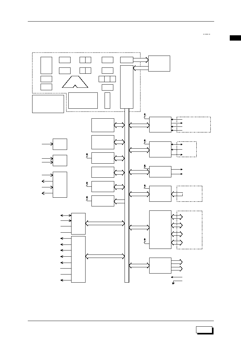
1.4 Block Diagram
Block diagrams of the ML63187, ML63189B, and ML63193 are shown in Figures 1-1, 1-2, and
1-3 respectively.
Asterisks (*) indicate port secondary functions. Signal names enclosed by chain lines (
)
indicate interface signals of the V
DDI
power supply system.
Figure 1-1 ML63187 Block Diagram
ROM
16KW
BUS
CON-
TROL
MIE
XT0
XT1
OSC0
OSC1
OSC
CBR
EBR
L
C
G
Z
ALU
RA
A
IR
INSTRUCTION
DECODER
RAM
1024N
nX-4/250
RESET
RST
V
DDI
PC
H
Y
X
TIMING
CON-
TROL
SP
RSP
STACK
CAL.S : 16 levels
REG.S : 16 levels
TIMER
8 bits
• 4
SCLK*
SIN*
SOUT*
4
INT
SFT
TM0CAP/TM1CAP*
TM0OVF/TM1OVF*
T02CK*
T13CK*
1
INT
I/O
PORT
PB.0≠PB.3
PE.0≠PE.3
2
INT
V
DDH
V
DD
CB1
CB2
DATA BUS
TBC
4
INT
BLD
INT
100HzTC
1
BACK-
UP
V
SS
MELODY
MD
1
INT
MDB
LCD
&
DSPR
COM1≠16
SEG0≠63
TST1
TST
TST2
INT
WDT
1
V
DD1
V
DD2
V
DD3
V
DD4
V
DD5
C1
C2
V
DDL
BIAS
INT187
CPU CORE
1-7
ML63187/189B/193 User's Manual
Chapter 1 Overview
1
M187
M189B
M193
Asterisks (*) indicate port secondary functions. Signal names enclosed by chain lines (
)
indicate interface signals of the V
DDI
power supply system.
XT0
XT1
OSC0
OSC1
OSC
RAM
1536N
RESET
RST
V
DDI
TIMER
8 bits
• 4
SCLK*
SIN*
SOUT*
4
INT
SFT
TM0CAP/TM1CAP*
TM0OVF/TM1OVF*
T02CK*
T13CK*
1
INT
I/O
PORT
P9.0≠P9.3
PA.0≠PA.3
PB.0≠PB.3
PE.0≠PE.3
2
INT
V
DDH
V
DD
CB1
CB2
DATA BUS
TBC
4
INT
BLD
INT
100HzTC
1
BACK-
UP
V
SS
MELODY
MD
1
INT
MDB
1
INT
INPUT
PORT
P0.0≠P0.3
LCD
&
DSPR
COM1≠16
SEG0≠63
TST1
TST
TST2
INT
WDT
1
V
DD1
V
DD2
V
DD3
V
DD4
V
DD5
C1
C2
V
DDL
BIAS
INT189
ROM
32KW
BUS
CON-
TROL
MIE
CBR
EBR
L
C
G
Z
ALU
RA
A
IR
INSTRUCTION
DECODER
nX-4/250
PC
H
Y
X
TIMING
CON-
TROL
SP
RSP
STACK
CAL.S : 16 levels
REG.S : 16 levels
CPU CORE
Figure 1-2 ML63189B Block Diagram
M189B

1-8
ML63187/189B/193 User's Manual
Chapter 1 Overview
M187
M189B
M193
Asterisks (*) indicate port secondary functions. Signal names enclosed by chain lines (
)
indicate interface signals of the V
DDI
power supply system.
Figure 1-3 ML63193 Block Diagram
XT0
XT1
OSC0
OSC1
OSC
RAM
2048N
RESET
RST
V
DDI
TIMER
8 bits
• 4
SCLK*
SIN*
SOUT*
4
INT
SFT
TM0CAP/TM1CAP*
TM0OVF/TM1OVF*
T02CK*
T13CK*
1
INT
I/O
PORT
P9.0≠P9.3
PA.0≠PA.3
PB.0≠PB.3
PC.0≠PC.3
PE.0≠PE.3
3
INT
V
DDH
V
DD
CB1
CB2
DATA BUS
TBC
4
INT
BLD
INT
100HzTC
1
BACK-
UP
V
SS
MELODY
MD
1
INT
MDB
1
INT
INPUT
PORT
P0.0≠P0.3
LCD
&
DSPR
COM1≠16
SEG0≠63
TST1
TST
TST2
INT
WDT
1
V
DD1
V
DD2
V
DD3
V
DD4
V
DD5
C1
C2
V
DDL
BIAS
INT193
ROM
64KW
BUS
CON-
TROL
MIE
CBR
EBR
L
C
G
Z
ALU
RA
A
IR
INSTRUCTION
DECODER
nX-4/250
PC
H
Y
X
TIMING
CON-
TROL
SP
RSP
STACK
CAL.S : 16 levels
REG.S : 16 levels
MULDIV
SIO
2
INT
RXC*
TXC*
RXD*
TXD*
CPU CORE
M193
1-9
ML63187/189B/193 User's Manual
Chapter 1 Overview
1
M187
M189B
M193
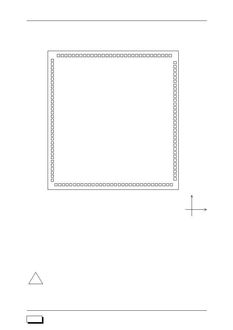
1.5 Pin Configuration
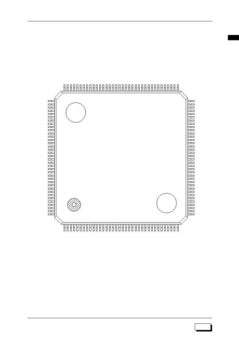
1.5.1 ML63187 Pin Configuration
The ML63187 pin configuration, chip pin configuration, and pad coordinates are shown in
Figures 1-4, 1-5, and Table 1-2, respectively.
NC (not connected) indicates an unused pin that is left unconnected (open).
Figure 1-4 ML63187 128-Pin QFP Pin Configuration (Top View)
1
2
3
4
5
6
7
8
9
10
11
12
13
14
15
16
17
18
19
20
21
22
23
24
25
26
27
28
29
30
31
32
33
34
35
36
37
38
102
101
100
99
98
97
96
95
94
93
92
91
90
89
88
87
86
85
84
83
82
81
80
79
78
77
76
75
74
73
72
71
70
69
68
67
66
65
103
104
105
106
107
108
109
110
111
112
113
114
115
116
117
118
119
120
121
122
123
124
125
126
127
128
64
63
62
61
60
59
58
57
56
55
54
53
52
51
50
49
48
47
46
45
44
43
42
41
40
39
SEG12
SEG13
SEG14
SEG15
SEG16
SEG17
SEG18
SEG19
SEG20
SEG21
SEG22
SEG23
SEG24
SEG25
SEG26
SEG27
SEG28
SEG29
SEG30
SEG31
SEG32
SEG33
SEG34
SEG35
SEG36
SEG37
(NC)
(NC)
(NC)
(NC)
SEG38
SEG39
SEG40
SEG41
SEG42
SEG43
SEG44
SEG45
SEG46
SEG47
SEG48
SEG49
SEG50
SEG51
SEG52
SEG53
SEG54
SEG55
SEG56
SEG57
SEG58
SEG59
SEG60
SEG61
SEG62
SEG63
COM9
COM10
COM11
COM12
(NC)
(NC)
(NC)
(NC)
MDB
MD
TST2
TST1
XT0
XT1
RESET
OSC0
OSC1
V
DDL
V
DD
CB2
CB1
V
DDH
C2
C1
V
DD5
V
DD4
V
DD3
V
DD2
V
DD1
V
SS
COM16
COM15
COM14
COM13
(NC)
(NC)
(NC)
(NC)
SEG11
SEG10
SEG9
SEG8
SEG7
SEG6
SEG5
SEG4
SEG3
SEG2
SEG1
SEG0
COM8
COM7
COM6
COM5
COM4
COM3
COM2
COM1
PB.3
PB.2
PB.1
PB.0
PE.3
PE.2
PE.1
PE.0
V
DDI
(NC)
(NC)
(NC)
(NC)
(NC)
M187

1-10
ML63187/189B/193 User's Manual
Chapter 1 Overview
M187
M189B
M193
∑ Chip size
: 4.238 mm
•
4.914 mm
∑ Chip thickness
: 350
m
m (280
m
m: available as required)
∑ Coordinate origin
: center of chip
∑ Pad hole size
: 100
m
m
•
100
m
m
∑ Pad size
: 110
m
m
•
110
m
m
∑ Minimum pad pitch
: 140
m
m
!
Note: The chip substrate voltage is V
SS
.
Figure 1-5 ML63187 Chip Pin Configuration (Top View)
Y
X
27 SEG38
28 SEG39
SEG11 111
29 SEG40
SEG10 110
30 SEG41
SEG9 109
31 SEG42
SEG8 108
32 SEG43
SEG7 107
33 SEG44
SEG6 106
34 SEG45
SEG5 105
35 SEG46
SEG4 104
36 SEG47
SEG3 103
37 SEG48
SEG2 102
38 SEG49
SEG1 101
39 SEG50
SEG0 100
40 SEG51
COM8 99
41 SEG52
COM7 98
42 SEG53
COM6 97
43 SEG54
COM5 96
44 SEG55
COM4 95
45 SEG56
COM3 94
46 SEG57
COM2 93
47 SEG58
COM1 92
48 SEG59
PB.3 91
49 SEG60
PB.2 90
50 SEG61
PB.1 89
SEG30 19
SEG29 18
57 COM13
SEG28 17
58 COM14
SEG27 16
59 COM15
SEG26 15
60 COM16
SEG25 14
61 V
SS
SEG24 13
62 V
DD1
SEG23 12
63 V
DD2
SEG22 11
64 V
DD3
SEG21 10
65 V
DD4
SEG20 9
66 V
DD5
SEG19 8
67 C1
SEG18 7
68 C2
SEG17 6
69 V
DDH
SEG16 5
70 CB1
SEG15 4
71 CB2
SEG14 3
72 V
DD
SEG13 2
73 V
DDL
SEG12 1
74 OSC1
75 OSC0
76 RESET
77 XT1
78 XT0
79 TST1
80 TST2
81 MD
82 MDB
SEG37 26
SEG36 25
SEG35 24
SEG34 23
SEG33 22
SEG32 21
SEG31 20
51 SEG62
PB.0 88
52 SEG63
PE.3 87
53 COM9
PE.2 86
54 COM10
PE.1 85
55 COM11
PE.0 84
56 COM12
V
DDI
83
ML63187
1-11
ML63187/189B/193 User's Manual
Chapter 1 Overview
1
M187
M189B
M193
M187
Table 1-2 ML63187 Pad Coordinates
Pad No.
Pad No.
Pad name
Pad name
X (
mm)
X (
mm)
Y (
mm)
Y (
mm)
Center of chip: x = 0, y = 0
1
2
3
4
5
6
7
8
9
10
11
12
13
14
15
16
17
18
19
20
21
22
23
24
25
26
27
28
29
30
31
32
33
34
35
36
37
38
39
40
SEG12
SEG13
SEG14
SEG15
SEG16
SEG17
SEG18
SEG19
SEG20
SEG21
SEG22
SEG23
SEG24
SEG25
SEG26
SEG27
SEG28
SEG29
SEG30
SEG31
SEG32
SEG33
SEG34
SEG35
SEG36
SEG37
SEG38
SEG39
SEG40
SEG41
SEG42
SEG43
SEG44
SEG45
SEG46
SEG47
SEG48
SEG49
SEG50
SEG51
41
42
43
44
45
46
47
48
49
50
51
52
53
54
55
56
57
58
59
60
61
62
63
64
65
66
67
68
69
70
71
72
73
74
75
76
77
78
79
80
SEG52
SEG53
SEG54
SEG55
SEG56
SEG57
SEG58
SEG59
SEG60
SEG61
SEG62
SEG63
COM9
COM10
COM11
COM12
COM13
COM14
COM15
COM16
V
SS
V
DD1
V
DD2
V
DD3
V
DD4
V
DD5
C1
C2
V
DDH
CB1
CB2
V
DD
V
DDL
OSC1
OSC0
RESET
XT1
XT0
TST1
TST2
≠1755
≠1615
≠1474
≠1334
≠1193
≠1053
≠913
≠772
≠632
≠491
≠351
≠211
≠70
70
211
351
491
632
772
913
1053
1193
1334
1474
1615
1755
1969
1969
1969
1969
1969
1969
1969
1969
1969
1969
1969
1969
1969
1969
≠2311
≠2311
≠2311
≠2311
≠2311
≠2311
≠2311
≠2311
≠2311
≠2311
≠2311
≠2311
≠2311
≠2311
≠2311
≠2311
≠2311
≠2311
≠2311
≠2311
≠2311
≠2311
≠2311
≠2311
≠2311
≠2311
≠2036
≠1895
≠1755
≠1615
≠1474
≠1334
≠1193
≠1053
≠913
≠772
≠632
≠491
≠351
≠211
1969
1969
1969
1969
1969
1969
1969
1969
1969
1969
1969
1969
1969
1969
1969
1969
1755
1615
1474
1334
1193
1053
913
772
632
491
351
211
70
≠70
≠211
≠351
≠491
≠632
≠772
≠913
≠1053
≠1193
≠1334
≠1474
≠70
70
211
351
491
632
772
913
1053
1193
1334
1474
1615
1755
1895
2036
2311
2311
2311
2311
2311
2311
2311
2311
2311
2311
2311
2311
2311
2311
2311
2311
2311
2311
2311
2311
2311
2311
2311
2311

1-12
ML63187/189B/193 User's Manual
Chapter 1 Overview
M187
M189B
M193
Table 1-2 ML63187 Pad Coordinates (continued)
Pad No.
Pad No.
Pad name
Pad name
X (
mm)
X (
mm)
Y (
mm)
Y (
mm)
Center of chip: x = 0, y = 0
81
82
83
84
85
86
87
88
89
90
91
92
93
94
95
96
MD
MDB
V
DDI
PE.0
PE.1
PE.2
PE.3
PB.0
PB.1
PB.2
PB.3
COM1
COM2
COM3
COM4
COM5
≠1615
≠1755
≠1969
≠1969
≠1969
≠1969
≠1969
≠1969
≠1969
≠1969
≠1969
≠1969
≠1969
≠1969
≠1969
≠1969
2311
2311
1895
1755
1615
1474
1334
1193
1053
913
772
632
491
351
211
70
97
98
99
100
101
102
103
104
105
106
107
108
109
110
111
COM6
COM7
COM8
SEG0
SEG1
SEG2
SEG3
SEG4
SEG5
SEG6
SEG7
SEG8
SEG9
SEG10
SEG11
≠1969
≠1969
≠1969
≠1969
≠1969
≠1969
≠1969
≠1969
≠1969
≠1969
≠1969
≠1969
≠1969
≠1969
≠1969
≠70
≠211
≠351
≠491
≠632
≠772
≠913
≠1053
≠1193
≠1334
≠1474
≠1615
≠1755
≠1895
≠2036

1-13
ML63187/189B/193 User's Manual
Chapter 1 Overview
1
M187
M189B
M193
1.5.2 ML63189B Pin Configuration
The ML63189B pin configuration, chip pin configuration, and pad coordinates are shown in
Figures 1-6, 1-7, and Table 1-3, respectively.
NC (not connected) indicates an unused pin that is left unconnected (open).
Figure 1-6 ML63189B 128-Pin QFP Pin Configuration (Top View)
1
2
3
4
5
6
7
8
9
10
11
12
13
14
15
16
17
18
19
20
21
22
23
24
25
26
27
28
29
30
31
32
33
34
35
36
37
38
102
101
100
99
98
97
96
95
94
93
92
91
90
89
88
87
86
85
84
83
82
81
80
79
78
77
76
75
74
73
72
71
70
69
68
67
66
65
103
104
105
106
107
108
109
110
111
112
113
114
115
116
117
118
119
120
121
122
123
124
125
126
127
128
64
63
62
61
60
59
58
57
56
55
54
53
52
51
50
49
48
47
46
45
44
43
42
41
40
39
SEG12
SEG13
SEG14
SEG15
SEG16
SEG17
SEG18
SEG19
SEG20
SEG21
SEG22
SEG23
SEG24
SEG25
SEG26
SEG27
SEG28
SEG29
(NC)
SEG30
SEG31
SEG32
SEG38
SEG39
SEG40
SEG41
SEG42
SEG43
SEG44
SEG45
SEG46
SEG47
SEG48
SEG49
SEG50
SEG51
SEG52
SEG53
SEG54
SEG55
SEG56
SEG57
SEG58
SEG59
SEG60
SEG61
SEG62
SEG63
COM9
COM10
(NC)
TST2
TST1
XT0
XT1
RESET
OSC0
OSC1
V
DDL
V
DD
CB2
CB1
V
DDH
C2
C1
V
DD5
V
DD4
V
DD3
V
DD2
V
DD1
V
SS
COM16
COM15
COM14
COM13
(NC)
SEG3
SEG2
SEG1
SEG0
COM8
COM7
COM6
COM5
COM4
COM3
COM2
COM1
P0.3
P0.2
P0.1
P0.0
P9.3
P9.2
P9.1
P9.0
PE.0
V
DDI
(NC)
MDB
MD
(NC)
SEG33
SEG34
SEG35
SEG36
SEG37
COM12
COM11
PA.3
PA.2
PA.1
PA.0
PB.3
PB.2
PB.1
PB.0
PE.3
PE.2
PE.1
SEG4
SEG5
SEG6
SEG7
SEG8
SEG9
SEG10
SEG11
M189B

1-14
ML63187/189B/193 User's Manual
Chapter 1 Overview
M187
M189B
M193
∑ Chip size
: 4.81 mm
•
5.20 mm
∑ Chip thickness
: 350
m
m (280
m
m: available as required)
∑ Coordinate origin
: center of chip
∑ Pad hole size
: 100
m
m
•
100
m
m
∑ Pad size
: 110
m
m
•
110
m
m
∑ Minimum pad pitch
: 140
m
m
!
Note: The chip substrate voltage is V
SS
.
Figure 1-7 ML63189B Chip Pin Configuration (Top View)
64 COM10
31 SEG32
Y
X
SEG1 123
92 MDB
SEG2 1
63 COM9
SEG31 30
32 SEG33
SEG0 122
33 SEG34
COM8 121
34 SEG35
COM7 120
35 SEG36
COM6 119
36 SEG37
COM5 118
37 SEG38
COM4 117
38 SEG39
COM3 116
39 SEG40
COM2 115
40 SEG41
COM1 114
41 SEG42
P0.3 113
42 SEG43
P0.2 112
43 SEG44
P0.1 111
44 SEG45
P0.0 110
45 SEG46
P9.3 109
46 SEG47
P9.2 108
47 SEG48
P9.1 107
48 SEG49
P9.0 106
49 SEG50
PA.3 105
50 SEG51
PA.2 104
51 SEG52
PA.1 103
52 SEG53
PA.0 102
53 SEG54
PB.3 101
54 SEG55
PB.2 100
55 SEG56
PB.1 99
56 SEG57
PB.0 98
57 SEG58
PE.3 97
58 SEG59
PE.2 96
59 SEG60
PE.1 95
60 SEG61
PE.0 94
61 SEG62
62 SEG63
V
DDI
93
SEG30 29
65 COM11
SEG29 28
66 COM12
SEG28 27
67 COM13
SEG27 26
68 COM14
SEG26 25
69 COM15
SEG25 24
70 COM16
SEG24 23
71 V
SS
SEG23 22
72 V
DD1
SEG22 21
73 V
DD2
SEG21 20
74 V
DD3
SEG20 19
75 V
DD4
SEG19 18
76 V
DD5
SEG18 17
77 C1
SEG17 16
78 C2
SEG16 15
79 V
DDH
SEG15 14
80 CB1
SEG14 13
81 CB2
SEG13 12
82 V
DD
SEG12 11
83 V
DDL
SEG11 10
84 OSC1
SEG10 9
85 OSC0
SEG9 8
86 RESET
SEG8 7
87 XT1
SEG7 6
88 XT0
SEG6 5
89 TST1
SEG5 4
90 TST2
SEG4 3
91 MD
SEG3 2
ML63189B
M189B
1-15
ML63187/189B/193 User's Manual
Chapter 1 Overview
1
M187
M189B
M193
Table 1-3 ML63189B Pad Coordinates
Pad No.
Pad No.
Pad name
Pad name
X (
mm)
X (
mm)
Y (
mm)
Center of chip: x = 0, y = 0
1
2
3
4
5
6
7
8
9
10
11
12
13
14
15
16
17
18
19
20
21
22
23
24
25
26
27
28
29
30
31
32
33
34
35
36
37
38
39
40
SEG2
SEG3
SEG4
SEG5
SEG6
SEG7
SEG8
SEG9
SEG10
SEG11
SEG12
SEG13
SEG14
SEG15
SEG16
SEG17
SEG18
SEG19
SEG20
SEG21
SEG22
SEG23
SEG24
SEG25
SEG26
SEG27
SEG28
SEG29
SEG30
SEG31
SEG32
SEG33
SEG34
SEG35
SEG36
SEG37
SEG38
SEG39
SEG40
SEG41
≠2259
≠1895
≠1755
≠1615
≠1474
≠1334
≠1193
≠1053
≠913
≠772
≠632
≠491
≠351
≠211
≠70
70
211
351
491
632
772
913
1053
1193
1334
1474
1615
1755
1895
2259
2259
2259
2259
2259
2259
2259
2259
2259
2259
2259
Y (
mm)
≠2438
≠2438
≠2438
≠2438
≠2438
≠2438
≠2438
≠2438
≠2438
≠2438
≠2438
≠2438
≠2438
≠2438
≠2438
≠2438
≠2438
≠2438
≠2438
≠2438
≠2438
≠2438
≠2438
≠2438
≠2438
≠2438
≠2438
≠2438
≠2438
≠2438
≠2176
≠2036
≠1895
≠1755
≠1615
≠1474
≠1334
≠1193
≠1053
≠913
41
42
43
44
45
46
47
48
49
50
51
52
53
54
55
56
57
58
59
60
61
62
63
64
65
66
67
68
69
70
71
72
73
74
75
76
77
78
79
80
SEG42
SEG43
SEG44
SEG45
SEG46
SEG47
SEG48
SEG49
SEG50
SEG51
SEG52
SEG53
SEG54
SEG55
SEG56
SEG57
SEG58
SEG59
SEG60
SEG61
SEG62
SEG63
COM9
COM10
COM11
COM12
COM13
COM14
COM15
COM16
V
SS
V
DD1
V
DD2
V
DD3
V
DD4
V
DD5
C1
C2
V
DDH
CB1
2259
2259
2259
2259
2259
2259
2259
2259
2259
2259
2259
2259
2259
2259
2259
2259
2259
2259
2259
2259
2259
2259
2259
1895
1755
1615
1474
1334
1193
1053
913
772
632
491
351
211
70
≠70
≠211
≠351
≠772
≠632
≠491
≠351
≠211
≠70
70
211
351
491
632
772
913
1053
1193
1334
1474
1615
1755
1895
2036
2176
2438
2438
2438
2438
2438
2438
2438
2438
2438
2438
2438
2438
2438
2438
2438
2438
2438
2438
M189B
1-16
ML63187/189B/193 User's Manual
Chapter 1 Overview
M187
M189B
M193
Table 1-3 ML63189B Pad Coordinates (continued)
Pad No.
Pad No.
Pad name
Pad name
X (
mm)
X (
mm)
Y (
mm)
Y (
mm)
Center of chip: x = 0, y = 0
81
82
83
84
85
86
87
88
89
90
91
92
93
94
95
96
97
98
99
100
101
102
CB2
V
DD
V
DDL
OSC1
OSC0
RESET
XT1
XT0
TST1
TST2
MD
MDB
V
DDI
PE.0
PE.1
PE.2
PE.3
PB.0
PB.1
PB.2
PB.3
PA.0
≠491
≠632
≠772
≠913
≠1053
≠1193
≠1334
≠1474
≠1615
≠1755
≠1895
≠2259
≠2259
≠2259
≠2259
≠2259
≠2259
≠2259
≠2259
≠2259
≠2259
≠2259
2438
2438
2438
2438
2438
2438
2438
2438
2438
2438
2438
2438
2132
1895
1755
1615
1474
1334
1193
1053
913
772
103
104
105
106
107
108
109
110
111
112
113
114
115
116
117
118
119
120
121
122
123
PA.1
PA.2
PA.3
P9.0
P9.1
P9.2
P9.3
P0.0
P0.1
P0.2
P0.3
COM1
COM2
COM3
COM4
COM5
COM6
COM7
COM8
SEG0
SEG1
≠2259
≠2259
≠2259
≠2259
≠2259
≠2259
≠2259
≠2259
≠2259
≠2259
≠2259
≠2259
≠2259
≠2259
≠2259
≠2259
≠2259
≠2259
≠2259
≠2259
≠2259
632
491
351
211
70
≠70
≠211
≠351
≠491
≠632
≠772
≠913
≠1053
≠1193
≠1334
≠1474
≠1615
≠1755
≠1895
≠2036
≠2176
M189B
1-17
ML63187/189B/193 User's Manual
Chapter 1 Overview
1
M187
M189B
M193
1
2
3
4
5
6
7
8
9
10
11
12
13
14
15
16
17
18
19
20
21
22
23
24
25
26
27
28
29
30
31
32
33
34
35
36
108
107
106
105
104
103
102
101
100
99
98
97
96
95
94
93
92
91
90
89
88
87
86
85
84
83
82
81
80
79
78
77
76
75
74
73
117
118
119
120
121
122
123
124
125
126
127
128
129
130
131
132
133
134
135
136
137
138
139
140
141
142
64
63
62
61
60
59
58
57
56
55
54
53
52
51
50
49
48
47
46
45
44
43
42
41
40
39
SEG22
SEG23
SEG24
SEG25
SEG26
SEG27
SEG28
SEG29
SEG30
SEG31
SEG32
SEG33
SEG34
SEG35
SEG36
SEG37
SEG38
SEG39
(NC)
(NC)
SEG40
SEG41
SEG47
SEG48
SEG49
SEG50
SEG51
SEG52
SEG53
SEG54
SEG55
SEG56
SEG57
SEG58
SEG59
SEG60
SEG61
SEG62
SEG63
COM9
COM10
COM11
COM12
COM13
COM14
COM15
COM16
(NC)
(NC)
PE.2
PE.1
PE.0
V
DDI
MDB
MD
TST2
TST1
XT0
XT1
RESET
OSC0
OSC1
V
DDL
V
DD
CB2
CB1
V
DDH
C2
C1
V
DD5
V
DD4
V
DD3
V
DD2
(NC)
SEG7
SEG6
SEG5
SEG4
SEG3
SEG2
SEG1
SEG0
COM8
COM7
COM6
COM5
COM4
COM3
COM2
COM1
V
SS
P0.3
P0.2
P0.1
PB.1
PB.0
(NC)
(NC)
SEG42
SEG43
SEG44
SEG45
SEG46
V
DD1
V
SS
P0.0
P9.3
P9.2
P9.1
P9.0
PA.3
PA.2
PA.1
PA.0
PB.3
PB.2
SEG14
SEG15
SEG16
SEG17
SEG18
SEG19
SEG20
SEG21
143
144
38
37
(NC)
(NC)
(NC)
(NC)
109
110
111
112
113
114
115
116
72
71
70
69
68
67
66
65
(NC)
(NC)
(NC)
PC.3
PC.2
PC.1
PC.0
PE.3
(NC)
(NC)
SEG8
SEG9
SEG10
SEG11
SEG12
SEG13
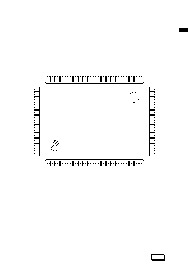
1.5.3 ML63193 Pin Configuration
The ML63193 pin configuration, chip pin configuration, and pad coordinates are shown in
Figures 1-8, 1-9, and Table 1-4, respectively.
NC (not connected) indicates an unused pin that is left unconnected (open).
Figure 1-8 ML63193 144-Pin LQFP Pin Configuration (Top View)
1-18
ML63187/189B/193 User's Manual
Chapter 1 Overview
M187
M189B
M193
∑ Chip size
: 5.72 mm
•
5.72 mm
∑ Chip thickness
: 350
m
m (280
m
m: available as required)
∑ Coordinate origin
: center of chip
∑ Pad hole size
: 100
m
m
•
100
m
m
∑ Pad size
: 110
m
m
•
110
m
m
∑ Minimum pad pitch
: 140
m
m
!
Note: The chip substrate voltage is V
SS
.
Figure 1-9 ML63193 Chip Pin Configuration (Top View)
Y
X
SEG8 1
SEG36 29
65 V
SS
SEG35 28
66 V
DD1
SEG34 27
67 V
DD2
SEG33 26
68 V
DD3
SEG32 25
69 V
DD4
SEG31 24
70 V
DD5
SEG30 23
71 C1
SEG29 22
72 C2
SEG28 21
73 V
DDH
SEG27 20
74 CB1
SEG26 19
75 CB2
SEG25 18
76 V
DD
SEG24 17
77 V
DDL
SEG23 16
78 OSC1
SEG22 15
79 OSC0
SEG21 14
80 RESET
SEG20 13
81 XT1
SEG19 12
82 XT0
SEG18 11
83 TST1
SEG17 10
84 TST2
SEG16 9
85 MD
SEG15 8
86 MDB
SEG14 7
87 V
DDI
SEG13 6
88 PE.0
SEG12 5
89 PE.1
SEG11 4
90 PE.2
SEG10 3
91 PE.3
SEG9 2
SEG39 32
SEG38 31
SEG37 30
92 PC.0
93 PC.1
94 PC.2
95 PC.3
ML63193
SEG2 123
SEG1 122
33 SEG40
SEG0 121
34 SEG41
COM8 120
35 SEG42
COM7 119
36 SEG43
COM6 118
37 SEG44
COM5 117
38 SEG45
COM4 116
39 SEG46
COM3 115
40 SEG47
COM2 114
41 SEG48
COM1 113
42 SEG49
V
SS
112
43 SEG50
P0.3 111
44 SEG51
P0.2 110
45 SEG52
P0.1 109
46 SEG53
P0.0 108
47 SEG54
P9.3 107
48 SEG55
P9.2 106
49 SEG56
P9.1 105
50 SEG57
P9.0 104
51 SEG58
PA.3 103
52 SEG59
PA.2 102
53 SEG60
PA.1 101
54 SEG61
PA.0 100
55 SEG62
PB.3 99
56 SEG63
PB.2 98
57 COM9
PB.1 97
58 COM10
PB.0 96
59 COM11
60 COM12
61 COM13
62 COM14
63 COM15
64 COM16
SEG7 128
SEG6 127
SEG5 126
SEG4 125
SEG3 124
M193

1-19
ML63187/189B/193 User's Manual
Chapter 1 Overview
1
M187
M189B
M193
Table 1-4 ML63193 Pad Coordinates
Pad No.
Pad No.
Pad name
Pad name
X (
mm)
X (
mm)
Y (
mm)
Y (
mm)
Center of chip: x = 0, y = 0
1
2
3
4
5
6
7
8
9
10
11
12
13
14
15
16
17
18
19
20
21
22
23
24
25
26
27
28
29
30
31
32
33
34
35
36
37
38
39
40
SEG8
SEG9
SEG10
SEG11
SEG12
SEG13
SEG14
SEG15
SEG16
SEG17
SEG18
SEG19
SEG20
SEG21
SEG22
SEG23
SEG24
SEG25
SEG26
SEG27
SEG28
SEG29
SEG30
SEG31
SEG32
SEG33
SEG34
SEG35
SEG36
SEG37
SEG38
SEG39
SEG40
SEG41
SEG42
SEG43
SEG44
SEG45
SEG46
SEG47
≠2204
≠2063
≠1923
≠1783
≠1642
≠1502
≠1361
≠1221
≠1081
≠940
≠800
≠659
≠519
≠379
≠238
≠98
43
183
323
464
604
745
885
1025
1166
1306
1447
1587
1727
1868
2008
2149
2714
2714
2714
2714
2714
2714
2714
2714
≠2714
≠2714
≠2714
≠2714
≠2714
≠2714
≠2714
≠2714
≠2714
≠2714
≠2714
≠2714
≠2714
≠2714
≠2714
≠2714
≠2714
≠2714
≠2714
≠2714
≠2714
≠2714
≠2714
≠2714
≠2714
≠2714
≠2714
≠2714
≠2714
≠2714
≠2714
≠2714
≠2149
≠2008
≠1868
≠1727
≠1587
≠1447
≠1306
≠1166
41
42
43
44
45
46
47
48
49
50
51
52
53
54
55
56
57
58
59
60
61
62
63
64
65
66
67
68
69
70
71
72
73
74
75
76
77
78
79
80
SEG48
SEG49
SEG50
SEG51
SEG52
SEG53
SEG54
SEG55
SEG56
SEG57
SEG58
SEG59
SEG60
SEG61
SEG62
SEG63
COM9
COM10
COM11
COM12
COM13
COM14
COM15
COM16
V
SS
V
DD1
V
DD2
V
DD3
V
DD4
V
DD5
C1
C2
V
DDH
CB1
CB2
V
DD
V
DDL
OSC1
OSC0
RESET
2714
2714
2714
2714
2714
2714
2714
2714
2714
2714
2714
2714
2714
2714
2714
2714
2714
2714
2714
2714
2714
2714
2714
2714
2152
2011
1871
1730
1590
1450
1309
1169
1028
888
748
607
467
326
186
46
≠1025
≠885
≠745
≠604
≠464
≠323
≠183
≠43
98
238
379
519
659
800
940
1081
1221
1361
1502
1642
1783
1923
2063
2204
2714
2714
2714
2714
2714
2714
2714
2714
2714
2714
2714
2714
2714
2714
2714
2714

1-20
ML63187/189B/193 User's Manual
Chapter 1 Overview
M187
M189B
M193
Table 1-4 ML63193 Pad Coordinates (continued)
Pad No.
Pad No.
Pad name
Pad name
X (
mm)
X (
mm)
Y (
mm)
Y (
mm)
Center of chip: x = 0, y = 0
81
82
83
84
85
86
87
88
89
90
91
92
93
94
95
96
97
98
99
100
101
102
103
104
XT1
XT0
TST1
TST2
MD
MDB
V
DDI
PE.0
PE.1
PE.2
PE.3
PC.0
PC.1
PC.2
PC.3
PB.0
PB.1
PB.2
PB.3
PA.0
PA.1
PA.2
PA.3
P9.0
≠95
≠235
≠376
≠516
≠656
≠797
≠937
≠1078
≠1218
≠1358
≠1499
≠1639
≠1780
≠1920
≠2060
≠2714
≠2714
≠2714
≠2714
≠2714
≠2714
≠2714
≠2714
≠2714
2714
2714
2714
2714
2714
2714
2714
2714
2714
2714
2714
2714
2714
2714
2714
2246
2106
1966
1825
1685
1544
1404
1264
1123
105
106
107
108
109
110
111
112
113
114
115
116
117
118
119
120
121
122
123
124
125
126
127
128
P9.1
P9.2
P9.3
P0.0
P0.1
P0.2
P0.3
V
SS
COM1
COM2
COM3
COM4
COM5
COM6
COM7
COM8
SEG0
SEG1
SEG2
SEG3
SEG4
SEG5
SEG6
SEG7
≠2714
≠2714
≠2714
≠2714
≠2714
≠2714
≠2714
≠2714
≠2714
≠2714
≠2714
≠2714
≠2714
≠2714
≠2714
≠2714
≠2714
≠2714
≠2714
≠2714
≠2714
≠2714
≠2714
≠2714
983
842
702
562
421
281
140
0
≠140
≠281
≠421
≠562
≠702
≠842
≠983
≠1123
≠1264
≠1404
≠1544
≠1685
≠1825
≠1966
≠2106
≠2246
M193
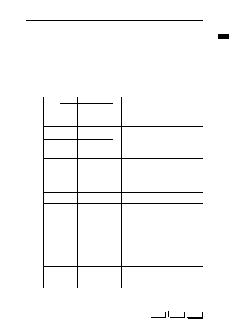
1-21
ML63187/189B/193 User's Manual
Chapter 1 Overview
1
M187
M189B
M193
1.6 Pin Descriptions
1.6.1 Descriptions of the Basic Functions of Each Pin
The basic functions of each pin of the ML63187, ML63189B, and ML63193 are listed in Table
1-5. Use of a slash ("/") in a pin name indicates that the pin has a secondary function. Refer
to section 1.6.2, "Descriptions of the Secondary Functions of Each Pin."
In the I/O column, "--" indicates a power supply pin, "I" indicates an input pin, "O" indicates
an output pin, and "I/O" indicates an input/output pin.
Table 1-5 Pin Description (Basic Functions)
Classification
Pin name
I/O
V
DD
--
V
SS
V
DD1
V
DD2
V
DD3
--
V
DD4
Power
Supply
V
DD5
C1
C2
--
V
DDI
--
V
DDL
--
V
DDH
--
CB1
--
CB2
XT0
I
Oscillator
XT1
O
OSC0
I
OSC1
O
Function
Positive power supply pin
Negative power supply pin
Power supply pins for LCD bias (internally generated):
Connect capacitors (0.1
mF) between these pins and V
SS
.
Capacitor connection pins for LCD bias generation:
Connect a capacitor (0.1
mF) between C1 and C2.
Positive power supply pin for external interface
(Power supply for input and I/O ports)
Positive power supply pin for internal logic (internally generated):
Connect a capacitor (0.1
mF) between pin and V
SS
.
Multiplied power supply pin for power supply backup (internally generated):
Connect a capacitor (1.0
mF) between pin and V
SS
.
Capacitor connection pins for multiplied power supply:
Connect a capacitor (1.0
mF) between CB1 and CB2.
Low-speed clock oscillation pins:
Crystal oscillation or RC oscillation is selected by
the mask option.
∑ If crystal oscillation is selected, connect a crystal
between XT0 and XT1, and connect capacitor (C
G
)
between XT0 and V
SS
.
∑ If RC oscillation is selected, connect external
oscillation resistor (R
OSL
) between XT0 and XT1.
High-speed clock oscillation pins:
Connect a ceramic resonator and capacitors (C
L0
, C
L1
)
or external oscillation resistor (R
OSH
) to these pins.
82
71
74
78
93
83
79
81
88
87
85
84
72
61
64
68
83
73
69
71
78
77
75
74
54
43
46
50
70
55
51
53
60
59
57
56
72
73
62
63
44
45
77
67
49
75
76
65
66
47
48
80
70
56
45
48
52
69
57
53
55
62
61
59
58
46
47
51
49
50
54
52
Pad
Pad
Pin
Pin
ML63189B
ML63187
76
65
112
68
72
87
77
73
75
82
81
79
78
50
39
91
42
46
61
51
47
49
56
55
53
52
66
67
40
41
71
45
69
70
43
44
74
48
Pad
Pin
ML63193
--
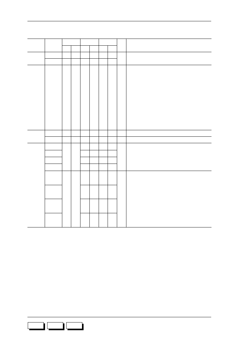
1-22
ML63187/189B/193 User's Manual
Chapter 1 Overview
M187
M189B
M193
Table 1-5 Pin Description (Basic Functions) (continued)
Classification
Pin name
I/O
P0.0/INT5
I
P9.0
I/O
Port
Function
4-bit input port:
Each bit can be selected as the following.
∑ Input with pull-up resistor
∑ Input with pull-down resistor
∑ High-impedance input
4-bit I/O port:
During the input mode, each bit can be selected as the following.
∑ Input with pull-up resistor
∑ Input with pull-down resistor
∑ High-impedance input
During the output mode, each bit can be selected as the following.
∑ P-channel open drain output
∑ N-channel open drain output
∑ CMOS output
∑ High-impedance output
P0.1/INT5
P0.2/INT5
P0.3/INT5
P9.1
P9.2
P9.3
--
--
--
--
110
106
111
112
113
107
108
109
ML63187 ML63189B
82
87
88
89
83
84
85
86
Pad
Pin
Pad
Pin
108
104
109
110
111
105
106
107
ML63193
83
88
89
90
84
85
86
87
Pad
Pin
TST1
I
Input pins for testing:
Pull-down resistors are built-in.
Test
TST2
RESET
I
Reset input pin:
Setting this pin to a "H" level causes internal circuitry
settings and values to be initialized. Next, if this pin is
set to a "L" level, the execution of instructions will begin
from address 0000H. A pull-down resistor is built-in.
An option of using RESET sampling circuit or not is
chosen by the mask option.
When using RESET sampling circuit, the system reset
mode is entered by holding the RESET pin at a "H" level
for 1 ms or more.
Reset
MD
O
Melody output pin (positive phase)
Melody
MDB
O
Melody output pin (reversed phase)
89
86
90
91
92
79
76
80
81
82
61
58
62
63
64
63
60
64
66
67
83
80
84
85
86
57
54
58
59
60
1-23
ML63187/189B/193 User's Manual
Chapter 1 Overview
1
M187
M189B
M193
Table 1-5 Pin Description (Basic Functions) (continued)
Classification
Pin name
I/O
Function
ML63189B
ML63187
Pad
Pin
Pad
Pin
ML63193
Pad
Pin
4-bit I/O port:
During the input mode, each bit can be selected as the following.
∑ Input with pull-up resistor
∑ Input with pull-down resistor
∑ High-impedance input
During the output mode, each bit can be selected as the following.
∑ P-channel open drain output
∑ N-channel open drain output
∑ CMOS output
∑ High-impedance output
PE.0/SIN
I/O
PE.1/SOUT
PE.2/SCLK
PE.3/INT2
71
72
73
74
84
85
86
87
94
95
96
97
70
71
72
73
88
89
90
91
62
63
64
65
Port
4-bit I/O port:
During the input mode, each bit can be selected as the following.
∑ Input with pull-up resistor
∑ Input with pull-down resistor
∑ High-impedance input
During the output mode, each bit can be selected as the following.
∑ P-channel open drain output
∑ N-channel open drain output
∑ CMOS output
∑ High-impedance output
PA.0
I/O
PA.1
PA.2
PA.3
PB.0/INT0/
TM0CAP/
TM0OVF/
I/O
PB.1/INT0/
TM1CAP/
TM1OVF
PB.2/INT0/
T02CK
PB.3/INT0/
T13CK
4-bit I/O port:
During the input mode, each bit can be selected as the following.
∑ Input with pull-up resistor
∑ Input with pull-down resistor
∑ High-impedance input
During the output mode, each bit can be selected as the following.
∑ P-channel open drain output
∑ N-channel open drain output
∑ CMOS output
∑ High-impedance output
I/O
--
75
76
77
78
--
88
89
90
91
102
103
104
105
98
99
100
101
78
79
80
81
74
75
76
77
100
101
102
103
96
97
98
99
92
93
94
95
79
80
81
82
75
76
77
78
66
67
68
69
PC.0/INT1/
RXD
PC.1/INT1/
TXC
PC.2/INT1/
RXC
PC.3/INT1/
TXD
--
--
--
--
1-24
ML63187/189B/193 User's Manual
Chapter 1 Overview
M187
M189B
M193
Table 1-5 Pin Description (Basic Functions) (continued)
Classification
Pin name
I/O
Function
ML63189B
ML63187
Pad
Pin
Pad
Pin
ML63193
Pad
Pin
SEG25
SEG26
24
14
116
25
15
117
124
125
18
19
128
129
SEG17
SEG18
SEG19
SEG20
SEG21
SEG22
SEG23
SEG24
16
6
108
17
7
109
18
8
110
19
9
111
20
10
112
21
11
113
22
12
114
23
13
116
117
118
119
120
121
122
123
115
10
120
11
121
12
122
13
123
14
124
15
125
16
126
17
127
LCD common signal output pins (COM1 to COM16)
LCD segment signal output pins (SEG0 to SEG26)
COM1
COM2
COM3
COM4
COM5
COM6
COM7
COM8
COM9
COM10
COM11
COM12
COM13
COM14
COM15
COM16
SEG0
SEG1
SEG2
SEG3
SEG4
SEG5
SEG6
SEG7
SEG8
SEG9
SEG10
SEG11
SEG12
SEG13
SEG14
SEG15
SEG16
LCD
O
O
114
92
79
115
93
80
116
94
81
117
95
82
118
96
83
119
97
84
120
98
85
121
99
86
63
53
31
64
54
32
65
55
33
66
56
34
67
57
39
68
58
40
69
59
41
70
60
42
122
100
87
123
101
88
1
102
89
2
103
90
3
104
91
4
105
92
5
106
93
6
107
94
7
108
95
8
109
96
9
110
97
10
111
98
11
1
103
12
2
104
13
3
105
14
4
106
15
5
107
90
91
92
93
94
95
96
97
36
37
39
40
41
42
43
44
98
99
100
101
103
104
105
106
107
108
109
110
111
112
113
114
115
113
92
114
93
115
94
116
95
117
96
118
97
119
98
120
99
57
27
58
28
59
29
60
30
61
31
62
32
63
33
64
34
121
100
122
101
123
102
124
103
125
104
126
105
127
106
128
107
1
111
2
112
3
113
4
114
5
115
6
116
7
117
8
118
9
119
1-25
ML63187/189B/193 User's Manual
Chapter 1 Overview
1
M187
M189B
M193
Table 1-5 Pin Description (Basic Functions) (continued)
Classification
Pin name
I/O
Function
SEG57
SEG58
SEG59
SEG60
SEG61
SEG62
SEG63
56
46
24
57
47
25
58
48
26
59
49
27
60
50
28
61
51
29
62
52
29
30
31
32
33
34
35
30
ML63189B
ML63187
Pad
Pin
Pad
Pin
50
51
52
53
54
55
56
20
21
22
23
24
25
26
ML63193
Pad
Pin
LCD
O
SEG27
SEG28
SEG29
SEG30
SEG31
SEG32
SEG33
SEG34
SEG35
SEG36
SEG37
SEG38
SEG39
SEG40
SEG41
SEG42
SEG43
SEG44
SEG45
SEG46
SEG47
SEG48
SEG49
SEG50
SEG51
SEG52
SEG53
SEG54
SEG55
SEG56
26
16
118
27
17
119
28
18
120
29
19
121
30
20
122
31
21
123
32
22
124
33
23
125
34
24
126
35
25
127
36
26
128
37
27
5
38
28
6
39
29
7
40
30
8
41
31
9
42
32
10
43
33
11
44
34
12
45
35
13
46
36
14
47
37
15
48
38
16
49
39
17
50
40
18
51
41
19
52
42
20
53
43
21
54
44
22
55
45
23
126
127
128
2
3
4
5
6
7
8
9
10
11
12
13
14
15
16
17
18
19
20
21
22
23
24
25
26
27
28
20
21
22
23
24
25
26
27
28
29
30
31
32
33
34
35
36
37
38
39
40
41
42
43
44
45
46
47
48
49
130
131
132
133
134
135
136
137
138
139
140
141
142
3
4
5
6
7
8
9
10
11
12
13
14
15
16
17
18
19
LCD segment signal output pins (SEG27 to SEG63)
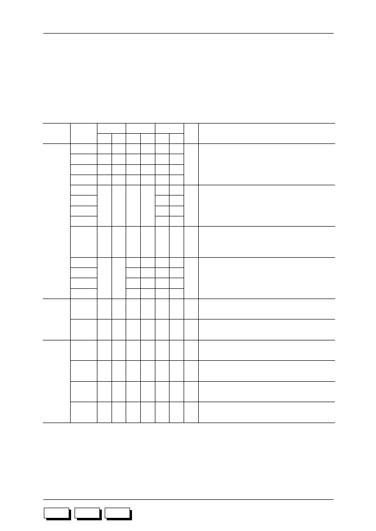
1-26
ML63187/189B/193 User's Manual
Chapter 1 Overview
M187
M189B
M193
1.6.2 Descriptions of the Secondary Functions of Each Pin
The secondary functions of each pin of the ML63187, ML63189B, and ML63193 are listed in
Table 1-6.
Table 1-6 Pin Description (Secondary Functions)
Classification
Pin name
I/O
PB.0/INT0
External
interrupt
I
Function
External interrupt 0 input pins:
Changes in the input signal level cause interrupts to be
generated. Interrupts can be enabled or disabled for
each bit by the port B interrupt enable register (PBIE).
PB.1/INT0
PB.2/INT0
PB.3/INT0
PE.3/INT2
I
External interrupt 2 input pin:
Changes in the input signal level cause interrupts to
be generated.
P0.0/INT5
I
External interrupt 5 input pins:
Changes in the input signal level cause interrupts to be
generated. Interrupts can be enabled or disabled for
each bit by the port 0 interrupt enable register (P0IE).
P0.1/INT5
P0.2/INT5
P0.3/INT5
PB.0/
TM0CAP
Capture
I
Timer 0 capture trigger input pin
PB.1/
TM1CAP
I
Timer 1 capture trigger input pin
PB.0/
TM0OVF
Timer
O
Timer 0 overflow flag output pin
PB.1/
TM1OVF
O
Timer 1 overflow flag output pin
PB.2/
T02CK
I
Timer 0, timer 2 external clock input pin
PB.3/
T13CK
I
Timer 1, timer 3 external clock input pin
75
76
77
78
74
--
75
76
75
76
77
78
74
75
76
77
73
86
87
88
89
74
75
74
75
76
77
88
89
90
91
87
--
88
89
88
89
90
91
98
99
100
101
97
110
111
112
113
98
99
98
99
100
101
ML63187 ML63189B
Pin Pad Pin Pad
75
76
77
78
65
87
88
89
90
75
76
75
76
77
78
96
97
98
99
91
108
109
110
111
96
97
96
97
98
99
ML63193
Pin Pad
PC.0/INT1
I
External interrupt 1 input pins:
Changes in the input signal level cause interrupts to be
generated. Interrupts can be enabled or disabled for
each bit by the port C interrupt enable register (PCIE).
PC.1/INT1
PC.2/INT1
PC.3/INT1
66
67
68
69
92
93
94
95
--
--
--
--

1-27
ML63187/189B/193 User's Manual
Chapter 1 Overview
1
M187
M189B
M193
Table 1-6 Pin Description (Secondary Functions) (continued)
Classification
Pin name
I/O
Function
PE.0/SIN
Shift
register
I
Shift register receive data input pin
PE.1/SOUT
O
Shift register transmit data output pin
PE.2/SCLK
I/O
Shift register clock input/output pin:
This pin should be configured as the clock output
when this device is used as the master processor,
or as the clock input when used as a slave.
71
72
73
70
71
72
84
85
86
94
95
96
ML63187 ML63189B
Pin Pad Pin Pad
62
63
64
88
89
90
ML63193
Pin Pad
PC.0/RXD
Serial
port
I
Serial port receive data input pin
PC.1/TXC
I/O
Synchronous serial port clock input/output pin:
This pin should be configured as the clock output for
transmit when this device is used as the master processor,
or as the clock input for transmit when used as a slave.
66
67
92
93
PC.2/RXC
I/O
Synchronous serial port clock input/output pin:
This pin should be configured as the clock output for
receive when this device is used as the master processor,
or as the clock input for receive when used as a slave.
--
--
--
--
68
94
PC.3/TXD
O
Serial port transmit data output pin
69
95

1-28
ML63187/189B/193 User's Manual
Chapter 1 Overview
M187
M189B
M193
!
Notes:
1. If a pin set as a high impedance input is left unconnected, the supply current may become
excessive. Therefore, it is recommended that unused input ports and input/output ports
be set as inputs with either a pull-down or pull-up resistor.
2. When test pins TST1 and TST2 are left unconnected, malfunction may result if there is a
large amount of external noise. Therefore, it is recommended to permanently connect
TST1 and TST2 to V
SS
.
3. Connect a capacitor (0.1
m
F) between the V
DD2
pin and the V
SS
pin when the LCD drivers
are not used.
1.6.3 Handling of Unused Pins
Table 1-7 shows how unused pins should be handled.
Table 1-7 Handling of Unused Pins
Pin
Recommended pin handling
OSC0, OSC1
Open
CB1, CB2
Open
TST1, TST2
Open or connect to V
SS
P0.0≠P0.3
Open
P9.0≠P9.3
Open
PA.0≠PA.3
Open
PB.0≠PB.3
Open
PE.0≠PE.3
Open
MD, MDB
Open
COM1≠COM16
Open
SEG0≠SEG63
Open
C1, C2
Open
V
DD1
, V
DD3
, V
DD4
, V
DD5
Open
PC.0≠PC.3
Open
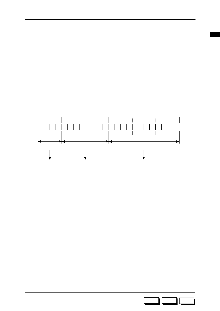
1-29
ML63187/189B/193 User's Manual
Chapter 1 Overview
1
M187
M189B
M193
1.7 Basic Timing
1.7.1 Basic Timing of CPU Operation
The low-speed oscillation clock from the XT0/XT1 pins or the high-speed oscillation clock
from the OSC0/OSC1 pins are used without frequency division as the system clock (CLK).
The system clock signal is in phase with the signal from the XT1 pin or the OSC1 pin.
As shown in Figure 1-10, a single machine cycle is composed of two states, S1 and S2. One
state is the interval from a falling edge of CLK to the falling edge of the next CLK.
Instructions are processed in machine cycle units and each instruction is executed in 1 to 3
machine cycles. Instructions are classified according to the number of machine cycles: 1
machine cycle instructions (M1), 2 machine cycle instructions (M1 + M2), and 3 machine cycle
instructions (M1 + M2 + M3).
Most instructions are executed in 1 machine cycle.
1.7.2 Port I/O Basic Timing
Figure 1-11 shows the basic I/O timing.
During the execution of an instruction that outputs data to a port, setting data (data A) is output
at the rising edge of the clock in the S2 state during the machine cycle of that instruction.
During the execution of an instruction that inputs data from a port, data at the input pin (data
B) is captured internally while the clock is at a "H" level in the S1 state during the machine cycle
of that instruction. That data is transferred to the accumulator at the start of the next machine
cycle.
Figure 1-10 Clock Configuration of Each Machine Cycle
CLK
M1
M1
M2
M1
M2
M3
S1
S2
S1
S2
S2
S1
S2
S1
S2
S1
S2
S1
(2 clocks)
(4 clocks)
(6 clocks)
1 machine cycle
2 machine cycles
3 machine cycles
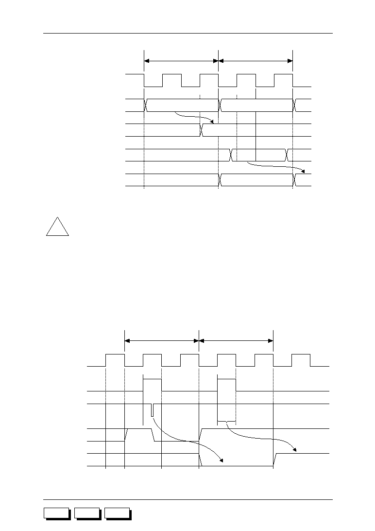
1-30
ML63187/189B/193 User's Manual
Chapter 1 Overview
M187
M189B
M193
Figure 1-12 Input Data Example
Figure 1-11 Port I/O Basic Timing
!
Note:
Regarding input signals
"0" will be captured in the internal register if a "L" level is input to the input pin even once (
q
of Figure 1-12) during the data capture interval.
"1" will be captured in the internal register only if a "H" level is maintained (
w
of Figure 1-12)
throughout the data capture interval.
Therefore, if noise occurs in the input data, implement noise reduction measures with the
program and peripheral devices.
MOV obj,(data A)
Output instruction
Input instruction
CLK
Instruction (example)
S1
S2
S1
S2
Output pin
Input pin
(data B)
Accumulator
(data B)
(data A)
MOV A,obj
Input instruction
Output instruction
CLK
Capture signal
S1
S2
S1
S2
Input pin
w
q
Data bus
Accumulator
"0"
"1"

1-31
ML63187/189B/193 User's Manual
Chapter 1 Overview
1
M187
M189B
M193
1.7.3 Interrupt Basic Timing
Figure 1-13 shows the basic interrupt timing.
As shown in the figure, when an interrupt factor is generated, the interrupt factor is sampled
at the falling edge of CLK and an interrupt request (IRQ) is set at the first half of S1.
When an interrupt condition is established and the CPU receives an interrupt, the interrupt
routine will start beginning from the next machine cycle.
Figure 1-13 Interrupt Basic Timing
M1
M1
CLK
Interrupt factor
S1
S2
S1
S2
S1
S2
IRQ
Process
Main routine
PC
1st interrupt address
Interrupt routine

1-32
ML63187/189B/193 User's Manual
Chapter 1 Overview
M187
M189B
M193

M189B
M187
M193
Chapter 2
CPU and Memory Spaces
2


2-1
ML63187/189B/193 User's Manual
Chapter 2 CPU and Memory Spaces
2
M187
M189B
M193
Chapter 2 CPU and Memory Spaces
2.1 Overview
The ML63187, ML63189B, and ML63193 have an internal Oki's original CPU core nX-4/250 core.
The instruction set of the nX-4/250 core consists of 408 types of instructions.
The memory space consists of a 16-bit wide program memory space and a 4-bit wide data
memory space. A stack for saving the program counter during a subroutine call or interrupt
(call stack) and a stack for saving registers during a PUSH instruction (register stack) are
provided separately from the memory space.
The program memory space is used for program data, ROM table data and melody note data.
In the data memory space, special function registers (SFRs) are located in BANK 0, the LCD
display register (DSPR) in BANK 1, and data RAM in BANKS 2 to 9 (BANKS 2 to 5 for the
ML63187, BANKS 2 to 7 for the ML63189B, and BANKS 2 to 9 for the ML63193).
2.2 Registers
The nX-4/250 core processes data mainly with the accumulator and register set.
The register set is a programming model consisting of the HL and XY registers that store data
memory addresses, the current bank register (CBR), the extra bank register (EBR), the RA
register that stores program memory addresses, registers that control program flow, and
registers that control flags and memory.
2.2.1 Accumulator (A)
The accumulator (A) is the central register for various arithmetic operations.
At system reset, the accumulator is initialized to "0". When an interrupt occurs, a "PUSH HL"
instruction can be used if necessary to save the accumulator on the register stack. The
accumulator can be restored with a "POP HL" instruction.
2.2.2 Flag Register
The flag register consists of 3 flags: the carry flag (C), the zero flag (Z) and the G flag (G).
When an interrupt occurs, a "PUSH HL" instruction can be used if necessary to save the flag
register on the register stack. The flag register can be restored with a "POP HL" instruction.
2.2.2.1 Carry Flag (C)
The carry flag (C) is a 1-bit flag that is loaded with a carry during addition or a borrow during
subtraction. At system reset, the carry flag is initialized to "0".
3
2
1
0
Accumulator
A
G
C
Z
Flag register

2-2
ML63187/189B/193 User's Manual
Chapter 2 CPU and Memory Spaces
M187
M189B
M193
2.2.2.2 Zero Flag (Z)
The zero flag (Z) is a 1-bit flag that is set to "1" when the contents of the accumulator (A) are
loaded with "0H". The zero flag is set to "0" when the contents of the accumulator (A) are
loaded with a value other than "0H". However, the XCH instruction does not change the zero
flag. At system reset, the zero flag is initialized to "0".
2.2.2.3 G Flag (G)
The G flag (G) changes to "1" when the HL, XY or RA registers overflow as the result of
execution of a post-increment register indirect addressing instruction or as the result of an
increment instruction for the HL, XY or RA registers. At system reset, the G flag is initialized
to "0".
2.2.3 Master Interrupt Enable Flag (MIE)
MIE (bit 0 of MIEF) is a flag that disables or enables all interrupts except for the watchdog timer
interrupt. MIEF is a 4-bit register in which bit 0 is the master interrupt enable flag (MIE).
If MIE is "0", all interrupts are disabled. If MIE is "1", all interrupts are enabled (with the
exception of the watchdog timer).
When any interrupt is received, MIE is cleared to "0". MIE is set to "1" by execution of a return
from interrupt instruction (RTI instruction).
If multi-level interrupt processing is to be performed, execute a RTI instruction (MIE
®
"1")
during the interrupt processing routines.
At system reset, MIE is initialized to "0". MIEF only supports data reference (R) of data
memory through addressing instructions.
!
Note:
When setting MIE, use "EI" instructions (MIE
®
"1") and "DI" instructions (MIE
®
"0").
--
--
--
MIE
MIEF (0FFH)
Master Interrupt Enable Flag
0: Interrupts disabled (initial value)
1: Interrupts enabled
bit 3
bit 2
bit 1
bit 0
(R)
2-3
ML63187/189B/193 User's Manual
Chapter 2 CPU and Memory Spaces
2
M187
M189B
M193
2.2.4 Current Bank Register (CBR), Extra Bank Register (EBR), HL Register (HL), XY
Register (XY)
The CBR, EBR, HL, and XY registers are used for indirect addressing of data memory.
The CBR and EBR registers indicate the data memory bank. The HL and XY registers indicate
addresses in the bank. CBR is also used in combination with 8-bit data in the instruction code
for direct addressing within the current bank.
Figure 2-1 shows the various register combinations.
CBR
CBR
EBR
EBR
CBR
H
L
X
Y
H
L
X
Y
Instruction code 8-bit data
+
+
+
+
A11≠A8
A7≠A4
A3≠A0
+
Figure 2-1 Various Register Combinations
A11 to A0 in Figure 2-1 indicate data memory addresses (4K nibbles max.).
At system reset, the CBR, EBR, HL, and XY registers are initialized to "0".
When an interrupt occurs, a "PUSH HL" or "PUSH XY" instruction can be used if necessary
to save the CBR, EBR, HL, and XY registers on the register stack. These registers can be
restored with a "POP HL" or "POP XY" instruction.
The CBR, EBR, HL, and XY registers are assigned to special function register (SFR)
addresses 0F9H to 0FEH.
e
3
e
2
e
1
e
0
EBR
bit 3
bit 2
bit 1
bit 0
c
3
c
2
c
1
c
0
CBR
bit 3
bit 2
bit 1
bit 0
H
bit 3
bit 2
bit 1
bit 0
L
bit 3
bit 2
bit 1
bit 0
h
3
h
2
h
1
h
0
l
3
l
2
l
1
l
0
X
bit 3
bit 2
bit 1
bit 0
Y
bit 3
bit 2
bit 1
bit 0
x
3
x
2
x
1
x
0
y
3
y
2
y
1
y
0
(0FDH)
(R/W)
(0FCH)
(R/W)
(0FBH)
(R/W)
(0FAH)
(R/W)
(0F9H)
(R/W)
(0FEH)
(R/W)

2-4
ML63187/189B/193 User's Manual
Chapter 2 CPU and Memory Spaces
M187
M189B
M193
2.2.5 Program Counter (PC)
The program counter (PC) is a counter with 16 valid bits that specifies the program memory
space.
2.2.6 RA Registers (RA3, RA2, RA1, RA0)
The RA registers are used for indirect program memory addressing (ROM table reference
instructions).
Figure 2-2 shows the address configuration of the RA registers.
At system reset, RA3 to RA0 are initialized to "0".
!
Note:
When executing a ROM table reference instruction that uses RA registers, do not use
addresses located in the SFR area to transfer ROM table data to RA registers, otherwise
indirect addressing of program memory will not operate properly.
RA3
RA2
RA1
RA0
A15≠A12
A11≠A8
A7≠A4
A3≠A0
Figure 2-2 Address Configuration of RA3 to RA0 Registers
Within the A15 to A0 of Figure 2-2, A14 to A0 indicate program memory addresses (32K
words max.).
RA3 to RA0 are assigned to special function register (SFR) addresses 0F2H to 0F5H.
a
15
a
14
a
13
a
12
RA3
bit 3
bit 2
bit 1
bit 0
a
11
a
10
a
9
a
8
RA2
bit 3
bit 2
bit 1
bit 0
RA1
bit 3
bit 2
bit 1
bit 0
RA0
bit 3
bit 2
bit 1
bit 0
a
7
a
6
a
5
a
4
a
3
a
2
a
1
a
0
(0F5H)
(R/W)
(0F4H)
(R/W)
(0F3H)
(R/W)
(0F2H)
(R/W)

2-5
ML63187/189B/193 User's Manual
Chapter 2 CPU and Memory Spaces
2
M187
M189B
M193
2.2.7 Stack Pointer (SP) and Call Stack
The stack pointer (SP) is a pointer that indicates the call stack address where the program
counter is saved when a subroutine call or interrupt occurs.
The SP is a 4-bit up/down counter that is incremented during stack saves and is decremented
during stack restores.
The call stack has 16 levels from address 0H to address 0FH. Because the hardware requires
1 level of the call stack during program execution, only 15 levels can be used for stack saves.
The contents of the call stack cannot be read or written by the program.
Figure 2-3 shows the relation between SP and the call stack.
3
2
1
0
SP
Stack pointer
Call stack
0FH
16 levels
0H
15 bits
Figure 2-3 Relation Between SP and Call Stack
SP is assigned to special function register (SFR) address 0F7H.
SP3
SP2
SP1
SP0
SP (0F7H)
(R)
bit 3
bit 2
bit 1
bit 0
At system reset, SP is initialized to "0" and points to address "0H" of the call stack. SP is a
read-only register and writes are invalid.
2-6
ML63187/189B/193 User's Manual
Chapter 2 CPU and Memory Spaces
M187
M189B
M193
2.2.8 Register Stack Pointer (RSP) and Register Stack
The register stack pointer (RSP) is a pointer that indicates the register stack address for
saving various registers.
RSP is a 4-bit up/down counter that is incremented during stack saves (execution of PUSH
instructions) and is decremented during stack restores (execution of POP instructions).
The register stack has 16 levels from address 0H to address 0FH. The contents of the register
stack cannot be read or written by the program.
Figure 2-4 shows the relation between RSP and the register stack.
2
1
0
RSP
Register stack pointer
Register stack
0FH
16 levels
0H
16 bits
3
Figure 2-4 Relation Between RSP and Register Stack
The various registers shown in Figure 2-5 are saved onto and restored from the register stack
by PUSH and POP instructions.
At system reset, RSP is initialized to "0" and points to address "0H" of the register stack.
rsp3
rsp2
rsp1
rsp0
RSP (0F6H)
bit 3
bit 2
bit 1
bit 0
(R/W)
L
H
A
Z
C
G
--
15
14
13
12
11
10
9
8
7
6
5
4
3
2
1
0
Register stack
"PUSH HL" and "POP HL" instruction execution
Y
X
CBR
EBR
15
14
13
12
11
10
9
8
7
6
5
4
3
2
1
0
Register stack
"PUSH XY" and "POP XY" instruction execution
Figure 2-5 Register Save/Restore by Execution of PUSH/POP Instructions
RSP is assigned to special function register (SFR) address 0F6H.

2-7
ML63187/189B/193 User's Manual
Chapter 2 CPU and Memory Spaces
2
M187
M189B
M193
2.3 Memory Spaces
2.3.1 Program Memory Space
The program memory space is the read-only memory that stores program data.
The program memory space has a data length of 16 bits and extends from address 0000H
to address 3FFFH in the ML63187, from address 0000H to address 7FFFH in the ML63189B,
and from address 0000H to address FFFFH in the ML63193.
In addition to program data, the program memory can also store ROM table data and the
melody data. Figure 2-6 shows the configuration of the program memory space.
Program data
or
ROM table data
or
Melody data
40 words
32,736 words
Interrupt area
0000H
0010H
0037H
7FFFH
32 words
7FDFH
ML63189B
Test data area
Program data
or
ROM table data
or
Melody data
40 words
16,352 words
Interrupt area
0000H
0010H
0037H
3FFFH
32 words
3FDFH
ML63187
Test data area
Program data
or
ROM table data
or
Melody data
40 words
65,504 words
Interrupt area
0000H
0010H
0037H
FFFFH
32 words
FFDFH
ML63193
Test data area
Figure 2-6 Program Memory Space Configuration
After system reset, instruction execution begins at address 0000H. The interrupt area from
address 0010H to address 0037H contains starting addresses of the interrupt processing
routines that are executed when interrupts are generated. (Refer to Chapter 4, "ML63187
Interrupt," Chapter 5, "ML63189B Interrupt," and Chapter 6, "ML63193 Interrupt.")
ROM table data is transferred to data memory by ROM table reference instructions.
The melody data defines the tone, tone length, and end tone used in the melody circuit of the
ML63187, ML63189B, and ML63193. After an MSA instruction specifies the starting address,
the melody data is automatically transferred to the melody circuit when a melody data
interrupt occurs. (Refer to Chapter 13, "Melody Driver.")
Because the test data area contains program data for testing, it cannot be used as a program
data area.

2-8
ML63187/189B/193 User's Manual
Chapter 2 CPU and Memory Spaces
M187
M189B
M193
2.3.2 Data Memory Space
The data memory space contains data RAM and special function registers (SFRs).
The data memory consists of 10 banks. One bank unit is 256 nibbles. BANK 0 is allocated
as a SFR area, BANK 1 as the LCD display register, and BANK 2 and the following BANKS
are data RAM.
Figure 2-7 shows the configuration of the data memory space.
BANK5
BANK2
BANK1
BANK0
5FFH
300H
2FFH
200H
1FFH
100H
0FFH
000H
Data RAM area
(1024 nibbles)
Display register
(256 nibbles)
SFR area
(256 nibbles)
ML63187
BANK3
400H
3FFH
500H
4FFH
BANK4
BANK5
BANK2
BANK1
BANK0
7FFH
300H
2FFH
200H
1FFH
100H
0FFH
000H
Data RAM area
(1536 nibbles)
Display register
(256 nibbles)
SFR area
(256 nibbles)
ML63189B
BANK3
400H
3FFH
500H
4FFH
BANK4
600H
5FFH
700H
6FFH
BANK6
BANK7
BANK5
BANK2
BANK1
BANK0
300H
2FFH
200H
1FFH
100H
0FFH
000H
Data RAM area
(2048 nibbles)
Display register
(256 nibbles)
SFR area
(256 nibbles)
ML63193
BANK3
400H
3FFH
500H
4FFH
BANK4
600H
5FFH
700H
6FFH
BANK6
BANK7
BANK8
BANK9
800H
7FFH
900H
8FFH
9FFH
Figure 2-7 Data Memory Space Configuration

M189B
M187
M193
CPU Control Functions
Chapter 3
3

3-1
ML63187/189B/193 User's Manual
Chapter 3 CPU Control Functions
3
M187
M189B
M193
Chapter 3 CPU Control Functions
3.1 Overview
Operating states, including system reset, are classified as follows.
∑ Normal operation mode
∑ System reset mode
∑ Halt mode
Figure 3-1 shows the CPU operating state transition diagram.
Figure 3-1 Operating State Transition Diagram
The normal operation mode is the state in which the CPU executes instructions sequentially.
The system reset mode begins when a reset input causes the CPU to begin system reset
processing where registers and pins are initialized. The CPU remains in this state until
instruction execution begins. After system reset processing, instruction execution begins
from address 0000H.
The halt mode is the state in which the CPU is halted (instruction execution suspended) but
internal peripheral functions continue to operate. During the halt mode, the PC is not
incremented. Even upon entering the halt mode, port and peripheral functions will not change.
Transfer to the halt mode is accomplished by executing a "HALT" instruction.
Normal operation
mode
Halt mode
System reset mode
RESET = "H"
RESET = "H"
RESET = "L"
Power on detect
Low-speed clock
oscillation halt detect
HALT instruction execution
Interrupt generated
3-2
ML63187/189B/193 User's Manual
Chapter 3 CPU Control Functions
M187
M189B
M193
3.2 System Reset Mode (RST)
3.2.1 Transfer to and State of System Reset Mode
The following three factors cause a transfer to the system reset mode.
∑ Setting the RESET pin to a "H" level
For the ML63193, since it has an internal reset sampling (2 kHz) circuit, the system
reset mode is entered by holding the RESET pin at a "H" level for 1 ms or more.
In the ML63193, whether the reset sampling circuit is used or not can be selected by
mask option.
∑ Detection of power on (not applied if the reset sampling circuit is used in the ML63193)
∑ Detection that low-speed clock oscillation is halted
The following operations are performed in the system reset mode.
(1) CPU is initialized.
(2) Backup flag changes to "1" and backup circuit changes to ON state.
(3) Bias reference voltage supply (VR) is energized.
(4) All LCD driver outputs are turned OFF and the outputs change to the V
SS
level.
(5) All special function registers (SFRs) are initialized. However, data RAM and display
registers are not initialized.
After system reset processing, instruction execution begins from address 0000H.
Figures 3-2 and 3-3 show the system reset generator circuit and Figure 3-4 shows the signals
when a system reset is generated.
Figure 3-2 ML63187/ML63189B/ML63193 (reset sampling circuit not used)
System Reset Generator Circuit
RESET
Power ON
detect
Low-speed
clock
oscillation
halt detect
R
Q
RESET0
(Time base
counter reset)
RESETS
(System reset)
4 Hz
S
V
SS
Low-speed
clock
oscillation
halt detect
R
Q
RESET0
(Time base
counter reset)
RESETS
(System reset)
4 Hz
S
V
SS
2 kHz
Sampling
circuit
RESET
Figure 3-3 ML63193 (reset sampling circuit used) System Reset Generator Circuit
3-3
ML63187/189B/193 User's Manual
Chapter 3 CPU Control Functions
3
M187
M189B
M193
Figure 3-4 Signals When System Reset is Generated
!
Note:
∑
System reset takes priority over all other processing and terminates all processing up to
that point in time. Therefore, the contents of RAM and display registers, which are not
initialized, cannot be guaranteed after a system reset.
∑
When the reset sampling circuit is used in the ML63193:
When setting the RESET pin to a "H" level to perform transfer to the system reset mode,
set the RESET pulse width to 1 ms or more.
RESET0
Crystal oscillation
output
RESETS
Backup
32.768 kHz
125 ms
ON
CPU start
62.5 ms
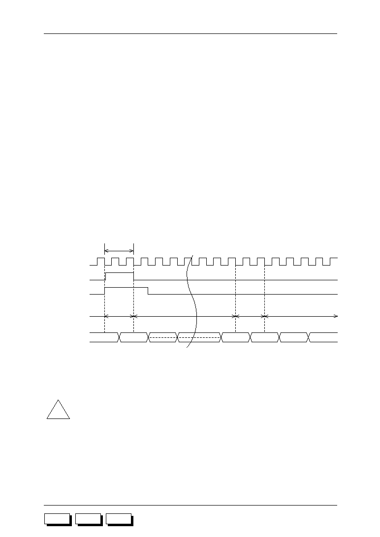
3-4
ML63187/189B/193 User's Manual
Chapter 3 CPU Control Functions
M187
M189B
M193
3.3 Halt Mode
3.3.1 Transfer to and State of Halt Mode
Transfer to the halt mode is performed by the software when a HALT instruction is executed.
When a HALT instruction is executed, the CPU enters the HALT mode at the S2 state of the
HALT instruction.
Oscillation and time base counter operation continue while in the halt mode.
If an interrupt request occurs at the same time as execution of a HALT instruction, interrupt
processing has priority and the HALT instruction will not be executed. After the HALT
instruction performs the equivalent operation of a NOP instruction, the interrupt routine is
entered. When an RTI instruction is used to complete the interrupt routine, the main routine
is resumed beginning from the instruction immediately following the HALT instruction.
Figure 3-5 shows the timing when a HALT instruction and interrupt request occur simultane-
ously.
S1
S2
S1
S2
S1
S2
S2
S1
S2
S1
S2
S1
S2
S1
S2
HALT
HALT
instruction
execution
RTI instruction
execution
HLT (halt flag)
Interrupt request
INT
PC flow in main
routine
: HALT instruction address
: Starting address of interrupt routine
: RTI instruction address
(equivalent
to NOP)
Interrupt routine
Main
routine
System clock
n
n+1
n+2
(INT)
(RTI)
n
(INT)
(RTI)
Figure 3-5 Timing of Simultaneous HALT Instruction and Interrupt Request
!
Note:
While an interrupt request is generated, execution of a HALT instruction will not transfer
operation to the halt mode.
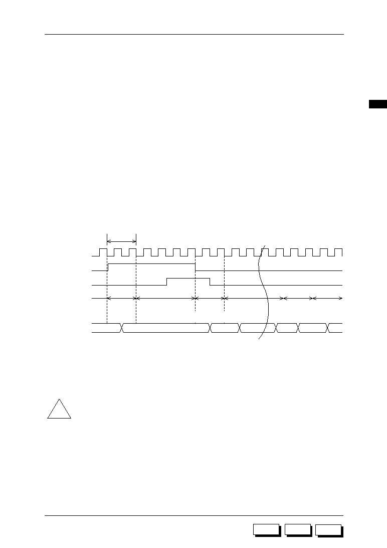
3-5
ML63187/189B/193 User's Manual
Chapter 3 CPU Control Functions
3
M187
M189B
M193
3.3.2 Halt Mode Release
The following two methods are available to release the halt mode.
∑ Release by interrupt generation (transfer to normal operation mode)
∑ Release by RESET pin (transfer to system reset mode)
3.3.2.1 Release of Halt Mode by Interrupt
If the halt mode is to be released by an interrupt, the enable flag of the interrupt used for
release must be set to "1" prior to entering the halt mode. When the halt mode is released by
an interrupt, operation transfers to the normal operation mode.
Figure 3-6 shows the timing of transferring to the halt mode by execution of a HALT instruction
and of releasing the halt mode by an interrupt.
When the halt mode is released by an interrupt request, the first instruction immediately
following the HALT instruction is executed and then the interrupt routine is entered. When an
RTI instruction is used to complete the interrupt routine, the main routine is resumed
beginning from the second instruction after the HALT instruction.
Figure 3-6 Timing of Transfer to Halt Mode and Release of Halt Mode by Interrupt
!
Note:
If the halt mode is to be released, set individual interrupt enable flags to "1". If an individual
interrupt enable flag is "0", the corresponding interrupt request signal cannot reset the HLT
flag, regardless of whether the master interrupt enable flag (MIE) is "0" or "1".
3.3.2.2 Release of Halt Mode by RESET Pin
If a high-level is input to the RESET pin, the CPU is released from the halt mode and transfers
to the system reset mode.
S1
S2
S1
S2
S1
S2
S1
S2
S1
S2
S1
S2
S1
S2
S1
S2
HALT
HLT (halt flag)
Interrupt request
INT
PC flow in main
routine
: HALT instruction address
: Starting address of interrupt routine
: RTI instruction address
HALT
instruction
execution
Halt mode
RTI
instruction
execution
Main
routine
Interrupt
routine
System clock
n
(RTI)
n+2
n+1
(INT)
n
(INT)
(RTI)
Execution of
instruction
immediately after
HALT instruction

3-6
ML63187/189B/193 User's Manual
Chapter 3 CPU Control Functions
M187
M189B
M193
3.3.3 Melody Data Interrupt and Halt Mode Release
The halt mode is not released by a melody data interrupt.
The melody data interrupt is different from a conventional interrupt in that the melody data
interrupt is a hardware processing interrupt used for transfer of melody data to the melody
circuit. It is not dependent on the program.
When this interrupt is generated, the instruction immediately after the HALT instruction is
executed, then the melody data is transferred to the melody circuit, and the HALT instruction
is executed again. This sequence is indicated in Figure 3-7.
S1
S2
S1
S2
S1
S2
S1
S2
S1
S2
S1
S2
S2
S2
S2
HALT
HALT
instruction
execution
n
HLT (halt flag)
Melody data
request
PC flow in main
routine
: HALT instruction address
: Melody data address
Halt mode
Halt mode
HALT
Melody
data
transfer
HALT
instruction
execution
(melody)
Execution of
instruction
immediately after
HALT instruction
n
System Clock
n+1
n+1
n
(melody)
Figure 3-7 Melody Data Request Interrupt Operation
3.3.4 Note Concerning HALT Instruction
As described above, the instruction immediately after the HALT instruction may be executed
any number of times. For this reason, always place an NOP instruction immediately after the
HALT instruction.
(Example)
∑
∑
∑
HALT
NOP
∑
∑
∑

M187
ML63187 Interrupt (INT187)
Chapter 4
4


4-1
ML63187/189B/193 User's Manual
Chapter 4 ML63187 Interrupt (INT187)
4
M187
Chapter 4 ML63187 Interrupt (INT187)
4.1 Overview
The ML63187 supports 14 interrupt factors: 2 external interrupts and 12 internal interrupts.
With the exception of the watchdog timer interrupt, interrupt enable/disable is controlled by
the master interrupt enable flag (MIE) and the individual interrupt enable registers (IE0 to IE4).
Watchdog timer interrupt is a non-maskable interrupt.
When interrupt conditions are met, the interrupt routine is executed from the interrupt start
address.
Table 4-1 indicates a list of interrupt factors, and Figure 4-1 shows the interrupt control
equivalent circuit.
Table 4-1 ML63187 Interrupt Factors
Priority
Interrupt factor
Symbol
Interrupt start address
1
Watchdog timer interrupt
WDTINT
0010H
2
Melody end interrupt
MDINT
0012H
3
External interrupt 0 (PB 4-bit OR input)
XI0INT
0014H
4
External interrupt 2 (PE.3)
XI2INT
0018H
5
6
7
Timer 0 interrupt
TM0INT
0020H
8
Timer 1 interrupt
TM1INT
0022H
9
Timer 2 interrupt
TM2INT
0024H
10
Timer 3 interrupt
TM3INT
0026H
11
Shift register interrupt
SFTINT
002CH
12
13
T10 Hz interrupt
T10HzINT
002EH
14
32 Hz interrupt
32HzINT
0030H
16 Hz interrupt
16HzINT
0032H
4 Hz interrupt
4HzINT
0034H
2 Hz interrupt
2HzINT
0036H
If multiple interrupts are detected simultaneously, the lowest interrupt start address is given
priority.
For details on interrupt operation, refer to Chapter 8 (Time Base Counter), Chapter 9 (Timers),
Chapter 10 (100 Hz Timer Counter), Chapter 11 (Watchdog Timer), Chapter 12 (Ports),
Chapter 13 (Melody Driver), and Chapter 15 (Shift Register).
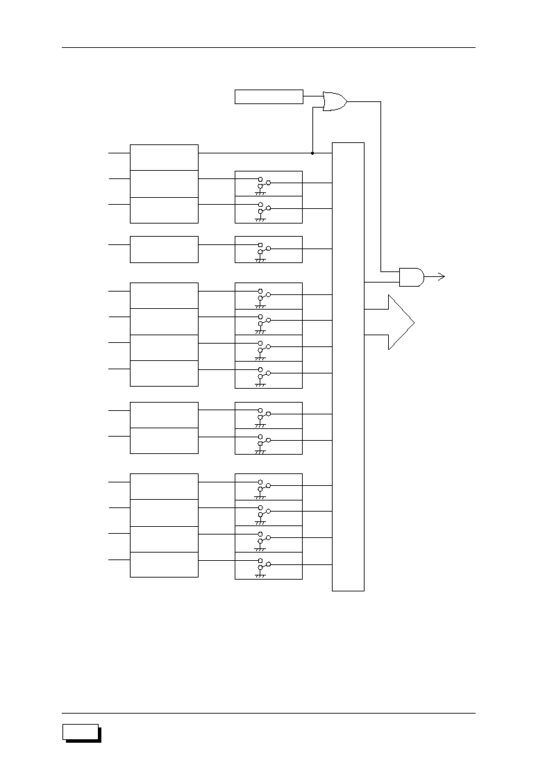
4-2
ML63187/189B/193 User's Manual
Chapter 4 ML63187 Interrupt (INT187)
M187
Interrupt request
signals
Interrupt request
registers
Interrupt enable registers
IRQ0.0
QWDT
IRQ0.2
QXI0
IRQ0.1
QMD
IE0.1
EMD
IE0.2
EXI0
IRQ0
IE0
MIE
Interrupt
vector address
Priority encoder
WDTINT
MDINT
XI0INT
IRQ1.0
QXI2
IRQ1
XI2INT
IE1.0
EXI2
IE1
IRQ2.0
QTM0
IRQ2.2
QTM2
IRQ2.1
QTM1
IRQ2.3
QTM3
IRQ2
TM0INT
TM1INT
TM2INT
TM3INT
IE2.0
ETM0
IE2.1
ETM1
IE2.2
ETM2
IE2.3
ETM3
IE2
IRQ3.2
QSFT
IRQ3.3
Q10Hz
IRQ3
SFTINT
T10HzINT
IE3.2
ESFT
IE3.3
E10Hz
IE3
IRQ4.0
Q32Hz
IRQ4.2
Q4Hz
IRQ4.1
Q16Hz
IRQ4.3
Q2Hz
IRQ4
32HzINT
16HzINT
4HzINT
2HzINT
IE4.0
E32Hz
IE4.1
E16Hz
IE4.2
E4Hz
IE4.3
E2Hz
IE4
Interrupt
request
Master interrupt enable flag
Figure 4-1 ML63187 Interrupt Control Equivalent Circuit
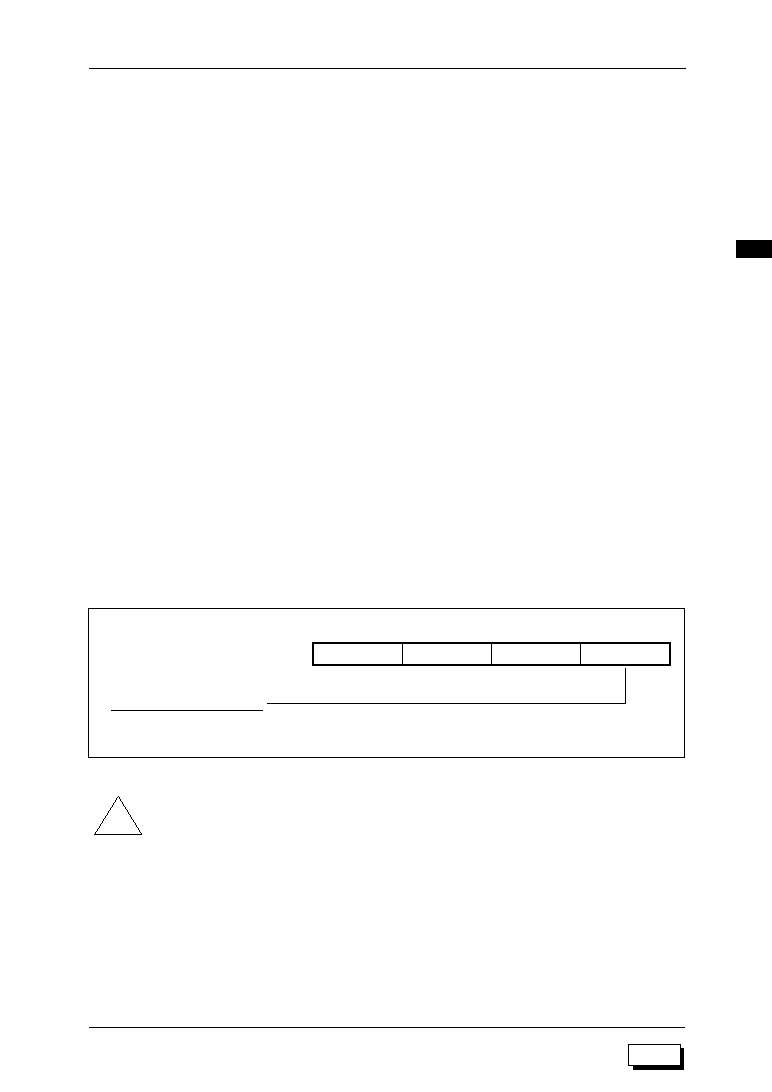
4-3
ML63187/189B/193 User's Manual
Chapter 4 ML63187 Interrupt (INT187)
4
M187
4.2 Interrupt Registers
The following three types of registers are used to control interrupts.
(1) Master interrupt enable register (MIEF)
(2) Interrupt enable registers (IE0 to IE4)
(3) Interrupt request registers (IRQ0 to IRQ4)
These registers are described below.
(1) Master interrupt enable register (MIEF)
MIEF is a 4-bit register in which bit 0 is the master interrupt enable flag (MIE).
MIE (bit 0 of MIEF) is a flag that disables or enables all interrupts except for the watchdog timer
interrupt.
If MIE is "0", all interrupts are disabled. If MIE is "1", all interrupts are enabled (with the
exception of the watchdog timer).
When any interrupt is received, MIE is cleared to "0". MIE is set to "1" by execution of a return
from interrupt instruction (RTI instruction).
If multi-level interrupt processing is to be performed, execute an RTI instruction (MIE
®
"1")
during the interrupt processing routines.
At system reset, MIE is initialized to "0". MIEF only supports data reference (R) of data
memory through addressing instructions.
--
--
--
MIE
MIEF
Master Interrupt Enable Flag
0: Interrupts disabled (initial value)
1: Interrupts enabled
bit 3
bit 2
bit 1
bit 0
(0FFH)
(R)
!
Note:
When setting MIE, use "EI" instructions (MIE
®
"1") and "DI" instructions (MIE
®
"0").

4-4
ML63187/189B/193 User's Manual
Chapter 4 ML63187 Interrupt (INT187)
M187
(2) Interrupt enable registers (IE0 to IE4)
IE0, IE1, IE2, IE3, and IE4 are registers that consist of 4 bits each.
A logical AND of the corresponding bits of an interrupt enable register (IE0 to IE4) and an
interrupt request register (IRQ0 to IRQ4) determines whether or not each interrupt request
is issued to the CPU. The watchdog timer interrupt is non-maskable, and is therefore not
dependent upon the interrupt enable registers (IE0 to IE4) and the master interrupt enable
register (MIEF).
If multiple interrupts request the CPU at the same time, as shown in Table 4-1, the interrupts
are accepted in order of highest priority and low priority interrupts are placed on hold.
When an interrupt is received, the master interrupt enable flag (MIE) is cleared to "0". The
corresponding bits in the interrupt enable registers (IE0 to IE4) do not change.
At system reset, each bit of IE0 through IE4 is initialized to "0".
--
--
--
EXI2
IE1
External interrupt 2 enable flag
0: Disable (initial value)
1: Enable
bit 3
bit 2
bit 1
bit 0
(051H)
(R/W)
--
EXI0
EMD
--
External interrupt 0 enable flag
0: Disable (initial value)
1: Enable
bit 3
bit 2
bit 1
bit 0
IE0 (050H)
(R/W)
Melody end interrupt enable flag
0: Disable (initial value)
1: Enable
ETM3
ETM2
ETM1
ETM0
Timer 3 interrupt enable flag
0: Disable (initial value)
1: Enable
bit 3
bit 2
bit 1
bit 0
Timer 2 interrupt enable flag
0: Disable (initial value)
1: Enable
Timer 1 interrupt enable flag
0: Disable (initial value)
1: Enable
Timer 0 interrupt enable flag
0: Disable (initial value)
1: Enable
IE2 (052H)
(R/W)
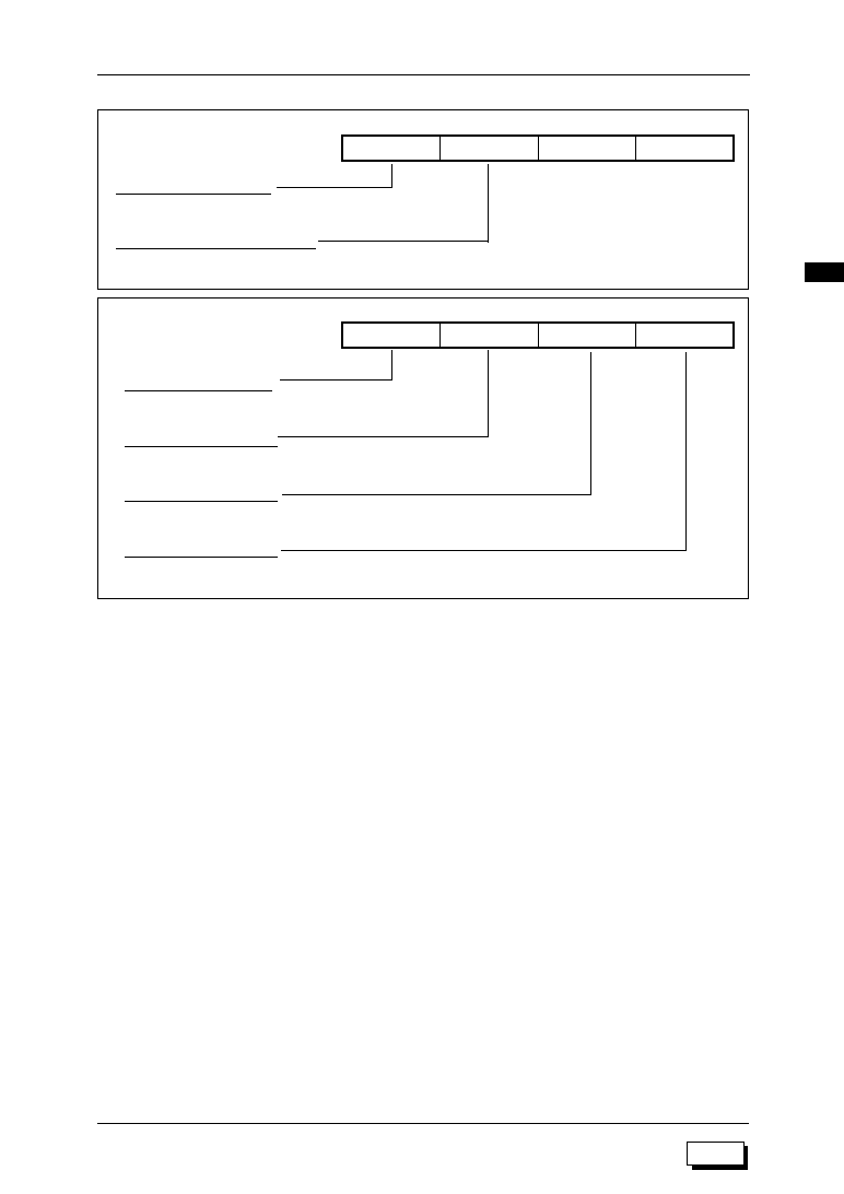
4-5
ML63187/189B/193 User's Manual
Chapter 4 ML63187 Interrupt (INT187)
4
M187
E10Hz
ESFT
--
--
10 Hz interrupt enable flag
0: Disable (initial value)
1: Enable
bit 3
bit 2
bit 1
bit 0
IE3 (053H)
(R/W)
Shift register interrupt enable flag
0: Disable (initial value)
1: Enable
E2Hz
E4Hz
E16Hz
E32Hz
2 Hz interrupt enable flag
0: Disable (initial value)
1: Enable
bit 3
bit 2
bit 1
bit 0
4 Hz interrupt enable flag
0: Disable (initial value)
1: Enable
16 Hz interrupt enable flag
0: Disable (initial value)
1: Enable
32 Hz interrupt enable flag
0: Disable (initial value)
1: Enable
IE4 (054H)
(R/W)
4-6
ML63187/189B/193 User's Manual
Chapter 4 ML63187 Interrupt (INT187)
M187
(3) Interrupt request registers (IRQ0 to IRQ4)
IRQ0, IRQ1, IRQ2, IRQ3 and IRQ4 are registers that consist of 4 bits each.
When an interrupt request is generated, the corresponding bit of the interrupt request register
is set to "1" in the first half of the S1 state of the next instruction. So that the CPU can receive
interrupt requests, set the master interrupt enable flag (MIE) to "1" and set the appropriate
flag of the corresponding interrupt enable register (IE0 to IE4) to "1".
The watchdog timer interrupt is non-maskable and does not depend upon the interrupt enable
register or the master interrupt enable register (MIEF).
Setting the appropriate bits of an interrupt request register to "1" allows software interrupts
to be generated.
When an interrupt request is received, the corresponding bits of IRQ0 to IRQ4 are cleared
to "0".
At system reset, each bit of IRQ0 through IRQ4 is initialized to "0".
bit 2: QXI0 (reQuest eXternal Interrupt 0)
The external interrupt 0 request flag.
The external interrupt 0 is assigned as the secondary function of each bit of port
B (PB.0 to PB.3). External interrupt 0 requests are generated by a 4-bit ORed input.
bit 1: QMD (reQuest Melody Driver)
Melody end interrupt request flag.
Melody end interrupts are generated when the melody driver outputs the end note
data (END bit = "1").
bit 0: QWDT (reQuest WatchDog Timer)
Watchdog timer interrupt request flag.
When the watchdog timer is started and then overflow occurs, an interrupt is
requested. The watchdog timer interrupt is non-maskable and does not depend
upon the interrupt enable registers or the master interrupt enable register (MIE).
--
QXI0
QMD
QWDT
bit 3
bit 2
bit 1
bit 0
External interrupt 0 request flag
0: No request (initial value)
1: Request
Melody end interrupt request flag
0: No request (initial value)
1: Request
Watchdog timer interrupt request flag
0: No request (initial value)
1: Request
IRQ0 (055H)
(R/W)
4-7
ML63187/189B/193 User's Manual
Chapter 4 ML63187 Interrupt (INT187)
4
M187
bit 0: QXI2 (reQuest eXternal Interrupt 2)
External interrupt 2 request flag.
The external interrupt 2 is assigned as a secondary function of port E.3 (PE.3).
Generation of the external interrupt 2 is triggered by the falling edge of the 128 Hz
or 4 kHz output of the time base counter.
--
--
--
QXI2
IRQ1
External interrupt 2 request flag
0: No request (initial value)
1: Request
bit 3
bit 2
bit 1
bit 0
(056H)
(R/W)
bit 3: QTM3 (reQuest TiMer 3)
Timer 3 interrupt request flag.
A timer 3 interrupt request is generated whenever timer 3 overflows.
bit 2: QTM2 (reQuest TiMer 2)
Timer 2 interrupt request flag.
A timer 2 interrupt request is generated whenever timer 2 overflows.
bit 1: QTM1 (reQuest TiMer 1)
Timer 1 interrupt request flag.
A timer 1 interrupt request is generated whenever timer 1 overflows.
bit 0: QTM0 (reQuest TiMer 0)
Timer 0 interrupt request flag.
A timer 0 interrupt request is generated whenever timer 0 overflows.
QTM3
QTM2
QTM1
QTM0
Timer 3 interrupt request flag
0: No request (initial value)
1: Request
bit 3
bit 2
bit 1
bit 0
Timer 2 interrupt request flag
0: No request (initial value)
1: Request
Timer 1 interrupt request flag
0: No request (initial value)
1: Request
Timer 0 interrupt request flag
0: No request (initial value)
1: Request
IRQ2 (057H)
(R/W)

4-8
ML63187/189B/193 User's Manual
Chapter 4 ML63187 Interrupt (INT187)
M187
Q10Hz
QSFT
--
--
10 Hz interrupt request flag
0: No request (initial value)
1: Request
bit 3
bit 2
bit 1
bit 0
IRQ3 (058H)
(R/W)
Shift register interrupt request flag
0: No request (initial value)
1: Request
Q2Hz
Q4Hz
Q16Hz
Q32Hz
2 Hz interrupt request flag
0: No request (initial value)
1: Request
bit 3
bit 2
bit 1
bit 0
4 Hz interrupt request flag
0: No request (initial value)
1: Request
16 Hz interrupt request flag
0: No request (initial value)
1: Request
32 Hz interrupt request flag
0: No request (initial value)
1: Request
IRQ4 (059H)
(R/W)
bit 3: Q2Hz (reQuest 2 Hz)
2 Hz interrupt request flag.
A 2 Hz interrupt request is generated at every falling edge of the 2 Hz output of the
time base counter.
bit 2: Q4Hz (reQuest 4 Hz)
4 Hz interrupt request flag.
A 4 Hz interrupt request is generated at every falling edge of the 4 Hz output of the
time base counter.
bit1: Q16Hz (reQuest 16 Hz)
16 Hz interrupt request flag.
A 16 Hz interrupt request is generated at every falling edge of the 16 Hz output of
the time base counter.
bit 0: Q32Hz (reQuest 32 Hz)
32 Hz interrupt request flag.
A 32 Hz interrupt request is generated at every falling edge of the 32 Hz output of
the time base counter.
bit 3: Q10Hz (reQuest 10 Hz)
10 Hz interrupt request flag.
A 10 Hz interrupt request is generated whenever the 10 Hz carry generated by the
100 Hz timer counter is output.
bit 2: QSFT (reQuest ShiFT register)
Shift register interrupt request flag.
A shift register interrupt is generated when the 8-bit data transfer for the shift
register is completed.

4-9
ML63187/189B/193 User's Manual
Chapter 4 ML63187 Interrupt (INT187)
4
M187
4.3 Interrupt Sequence
4.3.1 Interrupt Processing
While MIE is "1", operation transfers to interrupt processing when individual interrupt factors
are generated.
The watchdog timer interrupt is non-maskable and regardless of the MIE flag status,
operation will shift to interrupt processing when the watchdog timer interrupt factor is
generated.
The following processes are performed when an interrupt is generated.
(1) MIE and the corresponding interrupt request flag are cleared to "0".
(2) The program counter (PC) is saved on the call stack.
(3) The call stack pointer (SP) is incremented by 1. (SP
®
SP+1)
(4) The starting address of the interrupt routine is loaded into the program counter (PC).
Interrupt processing is performed in 0 machine cycles.
Figure 4-2 shows the stack contents after an interrupt is generated.
PC11≠PC8
PC7≠PC4
PC3≠PC0
0H
1H
2H
3H
4H
0FH
SP position before interrupt
SP position after interrupt
13 12 11 10 9 8 7 6 5 4 3 2 1 0
PC13≠
PC12
Figure 4-2 Call Stack Contents after Interrupt Generation

4-10
ML63187/189B/193 User's Manual
Chapter 4 ML63187 Interrupt (INT187)
M187
4.3.2 Return from an Interrupt Routine
Return from a watchdog timer interrupt routine is performed with an "RTNMI" instruction.
Return from all other interrupt routines is performed with an "RTI" instruction.
Execution of "RTI" and "RTNMI" instructions both require 1 machine cycle.
When returning from an interrupt routine, the CPU performs the following processes.
(1) The call stack pointer (SP) is decremented by 1. (SP
®
SP≠1)
(2) MIE is set to "1" (when an "RTNMI" instruction is used, MIE is restored to its state prior
to the interrupt).
(3) 1 is added to the call stack contents and that value is loaded into the program counter (PC).
!
Notes:
∑
While the MIE flag is "0" (interrupt disabled state), if a watchdog timer interrupt is
processed and an "RTI" instruction is executed, the MIE flag will be set to "1" and interrupts
enabled.
∑
Use "RTNMI" instructions to return from watchdog timer interrupts only. Use "RTI"
instructions for normal interrupts.
4.3.3 Interrupt Hold Instructions
Interrupt requests are not received after execution of interrupt hold instruction.
The interrupt hold instructions follow.
∑
ROM table reference instructions
∑
Stack operation instructions
∑
Jump instructions
∑
Conditional branch instructions
∑
Call/return instructions
∑
"EI" (set MIE flag) instructions, "DI" (clear MIE flag) instructions and "MSA cadr15" (start
melody output) instructions within control instructions
!
Note:
If interrupt hold instructions are used consecutively, even if an interrupt is generated, that
interrupt may be put on hold for a considerable amount of time before the interrupt routine
begins. Interrupt requests are received after execution of an instruction other than interrupt
hold instructions.

M189B
Chapter 5
5
ML63189B Interrupt (INT189)


5-1
M189B
ML63187/189B/193 User's Manual
Chapter 5 ML63189B Interrupt (INT189)
5
Chapter 5 ML63189B Interrupt (INT189)
5.1 Overview
The ML63189B supports 15 interrupt factors: 3 external interrupts and 12 internal interrupts.
With the exception of the watchdog timer interrupt, interrupt enable/disable is controlled by
the master interrupt enable flag (MIE) and the individual interrupt enable registers (IE0 to IE4).
Watchdog timer interrupt is a non-maskable interrupt.
When interrupt conditions are met, the interrupt routine is executed from the interrupt start
address.
Table 5-1 indicates a list of interrupt factors, and Figure 5-1 shows the interrupt control
equivalent circuit.
Table 5-1 ML63189B Interrupt Factors
Priority
Interrupt factor
Symbol
Interrupt start address
1
Watchdog timer interrupt
WDTINT
0010H
2
Melody end interrupt
MDINT
0012H
3
External interrupt 0 (PB 4-bit OR input)
XI0INT
0014H
4
External interrupt 2 (PE.3)
XI2INT
0018H
5
6
7
Timer 0 interrupt
TM0INT
0020H
8
Timer 1 interrupt
TM1INT
0022H
9
Timer 2 interrupt
TM2INT
0024H
10
Timer 3 interrupt
TM3INT
0026H
11
Shift register interrupt
SFTINT
002CH
12
13
T10 Hz interrupt
T10HzINT
002EH
14
32 Hz interrupt
32HzINT
0030H
16 Hz interrupt
16HzINT
0032H
4 Hz interrupt
4HzINT
0034H
2 Hz interrupt
2HzINT
0036H
15
External interrupt 5 (P0 4-bit OR input)
XI5INT
001EH
If multiple interrupts are detected simultaneously, the lowest interrupt start address is given
priority.
For details on interrupt operation, refer to Chapter 8 (Time Base Counter), Chapter 9 (Timers),
Chapter 10 (100 Hz Timer Counter), Chapter 11 (Watchdog Timer), Chapter 12 (Ports),
Chapter 13 (Melody Driver), and Chapter 15 (Shift Register).

5-2
ML63187/189B/193 User's Manual
Chapter 5 ML63189B Interrupt (INT189)
M189B
Interrupt request
signals
Interrupt request
registers
Interrupt enable registers
IRQ0.0
QWDT
IRQ0.2
QXI0
IRQ0.1
QMD
IE0.1
EMD
IE0.2
EXI0
IRQ0
IE0
MIE
Interrupt
vector address
Priority encoder
WDTINT
MDINT
XI0INT
IRQ1.0
QXI2
IRQ1
XI2INT
IE1.0
EXI2
IE1
IRQ2.0
QTM0
IRQ2.2
QTM2
IRQ2.1
QTM1
IRQ2.3
QTM3
IRQ2
TM0INT
TM1INT
TM2INT
TM3INT
IE2.0
ETM0
IE2.1
ETM1
IE2.2
ETM2
IE2.3
ETM3
IE2
IRQ3.2
QSFT
IRQ3.3
Q10Hz
IRQ3
SFTINT
T10HzINT
IE3.2
ESFT
IE3.3
E10Hz
IE3
IRQ4.0
Q32Hz
IRQ4.2
Q4Hz
IRQ4.1
Q16Hz
IRQ4.3
Q2Hz
IRQ4
32HzINT
16HzINT
4HzINT
2HzINT
IE4.0
E32Hz
IE4.1
E16Hz
IE4.2
E4Hz
IE4.3
E2Hz
IE4
Interrupt
request
Master interrupt enable flag
IRQ1.3
QXI5
XI5INT
IE1.3
EXI5
Figure 5-1 ML63189B Interrupt Control Equivalent Circuit

5-3
M189B
ML63187/189B/193 User's Manual
Chapter 5 ML63189B Interrupt (INT189)
5
5.2 Interrupt Registers
The following three types of registers are used to control interrupts.
(1) Master interrupt enable register (MIEF)
(2) Interrupt enable registers (IE0 to IE4)
(3) Interrupt request registers (IRQ0 to IRQ4)
These registers are described below.
(1) Master interrupt enable register (MIEF)
MIEF is a 4-bit register in which bit 0 is the master interrupt enable flag (MIE).
MIE (bit 0 of MIEF) is a flag that disables or enables all interrupts except for the watchdog timer
interrupt.
If MIE is "0", all interrupts are disabled. If MIE is "1", all interrupts are enabled (with the
exception of the watchdog timer).
When any interrupt is received, MIE is cleared to "0". MIE is set to "1" by execution of a return
from interrupt instruction (RTI instruction).
If multi-level interrupt processing is to be performed, execute an RTI instruction (MIE
®
"1")
during the interrupt processing routines.
At system reset, MIE is initialized to "0". MIEF only supports data reference (R) of data
memory through addressing instructions.
--
--
--
MIE
MIEF
Master Interrupt Enable Flag
0: Interrupts disabled (initial value)
1: Interrupts enabled
bit 3
bit 2
bit 1
bit 0
(0FFH)
(R)
!
Note:
When setting MIE, use "EI" instructions (MIE
®
"1") and "DI" instructions (MIE
®
"0").

5-4
ML63187/189B/193 User's Manual
Chapter 5 ML63189B Interrupt (INT189)
M189B
(2) Interrupt enable registers (IE0 to IE4)
IE0, IE1, IE2, IE3, and IE4 are registers that consist of 4 bits each.
A logical AND of the corresponding bits of an interrupt enable register (IE0 to IE4) and an
interrupt request register (IRQ0 to IRQ4) determines whether or not each interrupt request
is issued to the CPU. The watchdog timer interrupt is non-maskable, and is therefore not
dependent upon the interrupt enable registers (IE0 to IE4) and the master interrupt enable
register (MIEF).
If multiple interrupts request the CPU at the same time, as shown in Table 5-1, the interrupts
are accepted in order of highest priority and low priority interrupts are placed on hold.
When an interrupt is received, the master interrupt enable flag (MIE) is cleared to "0". The
corresponding bits in the interrupt enable registers (IE0 to IE4) do not change.
At system reset, each bit of IE0 through IE4 is initialized to "0".
--
EXI0
EMD
--
External interrupt 0 enable flag
0: Disable (initial value)
1: Enable
bit 3
bit 2
bit 1
bit 0
IE0 (050H)
(R/W)
Melody end interrupt enable flag
0: Disable (initial value)
1: Enable
EXI5
--
--
EXI2
External interrupt 5 enable flag
0: Disable (initial value)
1: Enable
bit 3
bit 2
bit 1
bit 0
IE1 (051H)
(R/W)
External interrupt 2 enable flag
0: Disable (initial value)
1: Enable

5-5
M189B
ML63187/189B/193 User's Manual
Chapter 5 ML63189B Interrupt (INT189)
5
E10Hz
ESFT
--
--
10 Hz interrupt enable flag
0: Disable (initial value)
1: Enable
bit 3
bit 2
bit 1
bit 0
IE3 (053H)
(R/W)
Shift register interrupt enable flag
0: Disable (initial value)
1: Enable
E2Hz
E4Hz
E16Hz
E32Hz
2 Hz interrupt enable flag
0: Disable (initial value)
1: Enable
bit 3
bit 2
bit 1
bit 0
4 Hz interrupt enable flag
0: Disable (initial value)
1: Enable
16 Hz interrupt enable flag
0: Disable (initial value)
1: Enable
32 Hz interrupt enable flag
0: Disable (initial value)
1: Enable
IE4 (054H)
(R/W)
ETM3
ETM2
ETM1
ETM0
Timer 3 interrupt enable flag
0: Disable (initial value)
1: Enable
bit 3
bit 2
bit 1
bit 0
Timer 2 interrupt enable flag
0: Disable (initial value)
1: Enable
Timer 1 interrupt enable flag
0: Disable (initial value)
1: Enable
Timer 0 interrupt enable flag
0: Disable (initial value)
1: Enable
IE2 (052H)
(R/W)

5-6
ML63187/189B/193 User's Manual
Chapter 5 ML63189B Interrupt (INT189)
M189B
(3) Interrupt request registers (IRQ0 to IRQ4)
IRQ0, IRQ1, IRQ2, IRQ3 and IRQ4 are registers that consist of 4 bits each.
When an interrupt request is generated, the corresponding bit of the interrupt request register
is set to "1" in the first half of the S1 state of the next instruction. So that the CPU can receive
interrupt requests, set the master interrupt enable flag (MIE) to "1" and set the appropriate
flag of the corresponding interrupt enable register (IE0 to IE4) to "1".
The watchdog timer interrupt is non-maskable and does not depend upon the interrupt enable
register or the master interrupt enable register (MIEF).
Setting the appropriate bits of an interrupt request register to "1" allows software interrupts
to be generated.
When an interrupt request is received, the corresponding bits of IRQ0 to IRQ4 are cleared
to "0".
At system reset, each bit of IRQ0 through IRQ4 is initialized to "0".
bit 2: QXI0 (reQuest eXternal Interrupt 0)
The external interrupt 0 request flag.
The external interrupt 0 is assigned as the secondary function of each bit of port
B (PB.0 to PB.3). External interrupt 0 requests are generated by a 4-bit ORed input.
bit 1: QMD (reQuest Melody Driver)
Melody end interrupt request flag.
Melody end interrupts are generated when the melody driver outputs the end note
data (END bit = "1").
bit 0: QWDT (reQuest WatchDog Timer)
Watchdog timer interrupt request flag.
When the watchdog timer is started and then overflow occurs, an interrupt is
requested. The watchdog timer interrupt is non-maskable and does not depend
upon the interrupt enable registers or the master interrupt enable register (MIE).
--
QXI0
QMD
QWDT
bit 3
bit 2
bit 1
bit 0
External interrupt 0 request flag
0: No request (initial value)
1: Request
Melody end interrupt request flag
0: No request (initial value)
1: Request
Watchdog timer interrupt request flag
0: No request (initial value)
1: Request
IRQ0 (055H)
(R/W)
5-7
M189B
ML63187/189B/193 User's Manual
Chapter 5 ML63189B Interrupt (INT189)
5
QXI5
--
--
QXI2
External interrupt 5 request flag
0: No request (initial value)
1: Request
bit 3
bit 2
bit 1
bit 0
IRQ1 (056H)
(R/W)
External interrupt 2 request flag
0: No request (initial value)
1: Request
bit 3: QXI5 (reQuest eXternal Interrupt 5)
External interrupt 5 request flag.
The external interrupt 5 is assigned as a secondary function to each bit (P0.0 to
0.3) of port 0.
An external interrupt request is generated through the 4-bit ORed input.
bit 0: QXI2 (reQuest eXternal Interrupt 2)
External interrupt 2 request flag.
The external interrupt 2 is assigned as a secondary function of port E.3 (PE.3).
Generation of the external interrupt 2 is triggered by the falling edge of the 128 Hz
or 4 kHz output of the time base counter.
bit 3: QTM3 (reQuest TiMer 3)
Timer 3 interrupt request flag.
A timer 3 interrupt request is generated whenever timer 3 overflows.
bit 2: QTM2 (reQuest TiMer 2)
Timer 2 interrupt request flag.
A timer 2 interrupt request is generated whenever timer 2 overflows.
bit 1: QTM1 (reQuest TiMer 1)
Timer 1 interrupt request flag.
A timer 1 interrupt request is generated whenever timer 1 overflows.
bit 0: QTM0 (reQuest TiMer 0)
Timer 0 interrupt request flag.
A timer 0 interrupt request is generated whenever timer 0 overflows.
QTM3
QTM2
QTM1
QTM0
Timer 3 interrupt request flag
0: No request (initial value)
1: Request
bit 3
bit 2
bit 1
bit 0
Timer 2 interrupt request flag
0: No request (initial value)
1: Request
Timer 1 interrupt request flag
0: No request (initial value)
1: Request
Timer 0 interrupt request flag
0: No request (initial value)
1: Request
IRQ2 (057H)
(R/W)

5-8
ML63187/189B/193 User's Manual
Chapter 5 ML63189B Interrupt (INT189)
M189B
Q10Hz
QSFT
--
--
10 Hz interrupt request flag
0: No request (initial value)
1: Request
bit 3
bit 2
bit 1
bit 0
IRQ3 (058H)
(R/W)
Shift register interrupt request flag
0: No request (initial value)
1: Request
Q2Hz
Q4Hz
Q16Hz
Q32Hz
2 Hz interrupt request flag
0: No request (initial value)
1: Request
bit 3
bit 2
bit 1
bit 0
4 Hz interrupt request flag
0: No request (initial value)
1: Request
16 Hz interrupt request flag
0: No request (initial value)
1: Request
32 Hz interrupt request flag
0: No request (initial value)
1: Request
IRQ4 (059H)
(R/W)
bit 3: Q2Hz (reQuest 2 Hz)
2 Hz interrupt request flag.
A 2 Hz interrupt request is generated at every falling edge of the 2 Hz output of the
time base counter.
bit 2: Q4Hz (reQuest 4 Hz)
4 Hz interrupt request flag.
A 4 Hz interrupt request is generated at every falling edge of the 4 Hz output of the
time base counter.
bit1: Q16Hz (reQuest 16 Hz)
16 Hz interrupt request flag.
A 16 Hz interrupt request is generated at every falling edge of the 16 Hz output of
the time base counter.
bit 0: Q32Hz (reQuest 32 Hz)
32 Hz interrupt request flag.
A 32 Hz interrupt request is generated at every falling edge of the 32 Hz output of
the time base counter.
bit 3: Q10Hz (reQuest 10 Hz)
10 Hz interrupt request flag.
A 10 Hz interrupt request is generated whenever the 10 Hz carry generated by the
100 Hz timer counter is output.
bit 2: QSFT (reQuest ShiFT register)
Shift register interrupt request flag.
A shift register interrupt is generated when the 8-bit data transfer for the shift
register is completed.

5-9
M189B
ML63187/189B/193 User's Manual
Chapter 5 ML63189B Interrupt (INT189)
5
5.3 Interrupt Sequence
5.3.1 Interrupt Processing
While MIE is "1", operation transfers to interrupt processing when individual interrupt factors
are generated.
The watchdog timer interrupt is non-maskable and regardless of the MIE flag status,
operation will shift to interrupt processing when the watchdog timer interrupt factor is
generated.
The following processes are performed when an interrupt is generated.
(1) MIE and the corresponding interrupt request flag are cleared to "0".
(2) The program counter (PC) is saved on the call stack.
(3) The call stack pointer (SP) is incremented by 1. (SP
®
SP+1)
(4) The starting address of the interrupt routine is loaded into the program counter (PC).
Interrupt processing is performed in 0 machine cycles.
Figure 5-2 shows the stack contents after an interrupt is generated.
PC11≠PC8
PC7≠PC4
PC3≠PC0
0H
1H
2H
3H
4H
0FH
SP position before interrupt
SP position after interrupt
13 12 11 10 9 8 7 6 5 4 3 2 1 0
PC13≠
PC12
Figure 5-2 Call Stack Contents after Interrupt Generation

5-10
ML63187/189B/193 User's Manual
Chapter 5 ML63189B Interrupt (INT189)
M189B
5.3.2 Return from an Interrupt Routine
Return from a watchdog timer interrupt routine is performed with an "RTNMI" instruction.
Return from all other interrupt routines is performed with an "RTI" instruction.
Execution of "RTI" and "RTNMI" instructions both require 1 machine cycle.
When returning from an interrupt routine, the CPU performs the following processes.
(1) The call stack pointer (SP) is decremented by 1. (SP
®
SP≠1)
(2) MIE is set to "1" (when an "RTNMI" instruction is used, MIE is restored to its state prior
to the interrupt).
(3) 1 is added to the call stack contents and that value is loaded into the program counter (PC).
!
Notes:
∑
While the MIE flag is "0" (interrupt disabled state), if a watchdog timer interrupt is
processed and an "RTI" instruction is executed, the MIE flag will be set to "1" and interrupts
enabled.
∑
Use "RTNMI" instructions to return from watchdog timer interrupts only. Use "RTI"
instructions for normal interrupts.
5.3.3 Interrupt Hold Instructions
Interrupt requests are not received after execution of interrupt hold instruction.
The interrupt hold instructions follow.
∑
ROM table reference instructions
∑
Stack operation instructions
∑
Jump instructions
∑
Conditional branch instructions
∑
Call/return instructions
∑
"EI" (set MIE flag) instructions, "DI" (clear MIE flag) instructions and "MSA cadr15" (start
melody output) instructions within control instructions
!
Note:
If interrupt hold instructions are used consecutively, even if an interrupt is generated, that
interrupt may be put on hold for a considerable amount of time before the interrupt routine
begins. Interrupt requests are received after execution of an instruction other than interrupt
hold instructions.

M193
ML63193 Interrupt (INT193)
Chapter 6
6


6-1
ML63187/189B/193 User's Manual
Chapter 6 ML63193 Interrupt (INT193)
6
M193
Chapter 6 ML63193 Interrupt (INT193)
6.1 Overview
The ML63193 supports 18 interrupt factors: 4 external interrupts and 14 internal interrupts.
With the exception of the watchdog timer interrupt, interrupt enable/disable is controlled by
the master interrupt enable flag (MIE) and the individual interrupt enable registers (IE0 to IE4).
Watchdog timer interrupt is a non-maskable interrupt.
When interrupt conditions are met, the interrupt routine is executed from the interrupt start
address.
Table 6-1 indicates a list of interrupt factors, and Figure 6-1 shows the interrupt control
equivalent circuit.
Table 6-1 ML63193 Interrupt Factors
If multiple interrupts are detected simultaneously, the lowest interrupt start address is given
priority.
For details on interrupt operation, refer to Chapter 8 (Time Base Counter), Chapter 9 (Timers),
Chapter 10 (100 Hz Timer Counter), Chapter 11 (Watchdog Timer), Chapter 12 (Ports),
Chapter 13 (Melody Driver), Chapter 14 (Serial Port), and Chapter 15 (Shift Register).
Priority
Interrupt factor
Symbol
Interrupt start address
1
Watchdog timer interrupt
WDTINT
0010H
2
Melody end interrupt
MDINT
0012H
3
External interrupt 0 (PB 4-bit OR input)
XI0INT
0014H
5
External interrupt 2 (PE.3)
XI2INT
0018H
6
7
8
Timer 0 interrupt
TM0INT
0020H
9
Timer 1 interrupt
TM1INT
0022H
10
Timer 2 interrupt
TM2INT
0024H
13
Timer 3 interrupt
TM3INT
0026H
14
Shift register interrupt
SFTINT
002CH
15
16
T10 Hz interrupt
T10HzINT
002EH
17
32 Hz interrupt
32HzINT
0030H
16 Hz interrupt
16HzINT
0032H
4 Hz interrupt
4HzINT
0034H
2 Hz interrupt
2HzINT
0036H
18
External interrupt 5 (P0 4-bit OR input)
XI5INT
001EH
4
External interrupt 1 (PC 4-bit OR input)
XI1INT
0016H
11
Serial port receive interrupt
SRINT
0028H
12
Serial port transmit interrupt
STINT
002AH
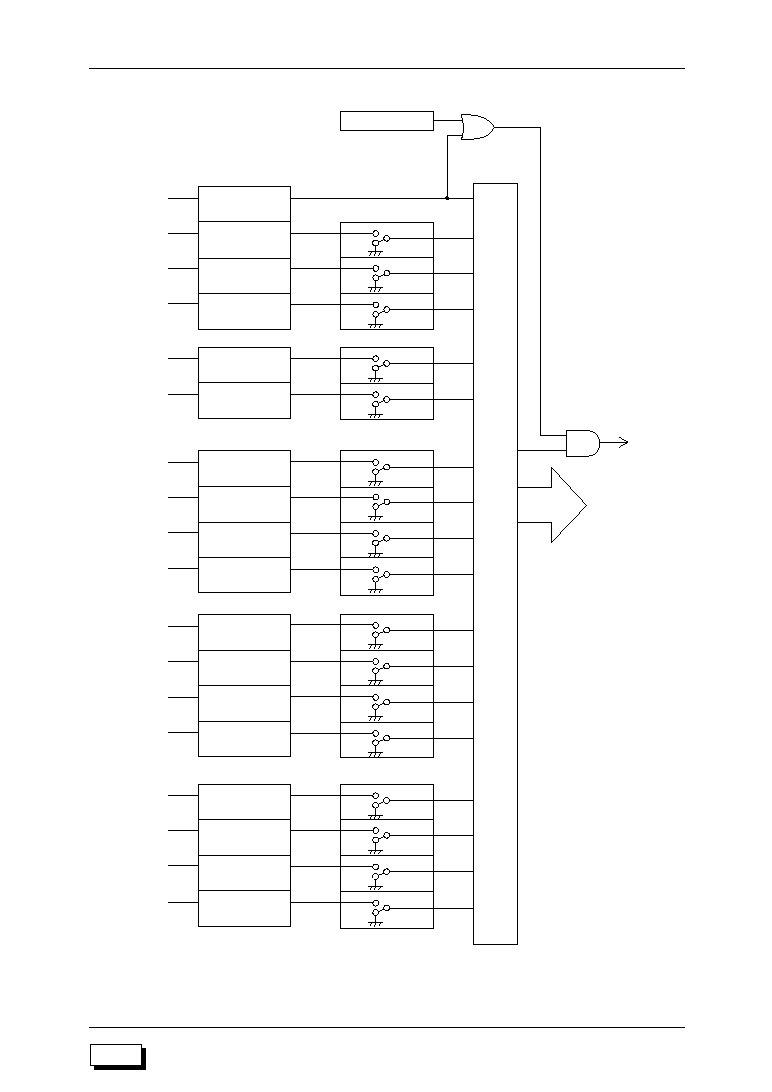
M193
6-2
ML63187/189B/193 User's Manual
Chapter 6 ML63193 Interrupt (INT193)
Interrupt request
signals
Interrupt request
registers
Interrupt enable registers
IRQ0.0
QWDT
IRQ0.2
QXI0
IRQ0.1
QMD
IE0.1
EMD
IE0.2
EXI0
IRQ0
IE0
MIE
Interrupt
vector address
Priority encoder
WDTINT
MDINT
XI0INT
IRQ1.0
QXI2
IRQ1
XI2INT
IE1.0
EXI2
IE1
IRQ2.0
QTM0
IRQ2.2
QTM2
IRQ2.1
QTM1
IRQ2.3
QTM3
IRQ2
TM0INT
TM1INT
TM2INT
TM3INT
IE2.0
ETM0
IE2.1
ETM1
IE2.2
ETM2
IE2.3
ETM3
IE2
IRQ3.2
QSFT
IRQ3.3
Q10Hz
IRQ3
SFTINT
T10HzINT
IE3.2
ESFT
IE3.3
E10Hz
IE3
IRQ4.0
Q32Hz
IRQ4.2
Q4Hz
IRQ4.1
Q16Hz
IRQ4.3
Q2Hz
IRQ4
32HzINT
16HzINT
4HzINT
2HzINT
IE4.0
E32Hz
IE4.1
E16Hz
IE4.2
E4Hz
IE4.3
E2Hz
IE4
Interrupt
request
Master interrupt enable flag
IRQ1.3
QXI5
XI5INT
IE1.3
EXI5
IRQ0.3
QXI1
IE0.3
EXI1
XI1INT
IE3.0
ESR
IE3.1
EST
IRQ3.0
QSR
IRQ3.1
QST
SRINT
STINT
Figure 6-1 ML63193 Interrupt Control Equivalent Circuit
6-3
ML63187/189B/193 User's Manual
Chapter 6 ML63193 Interrupt (INT193)
6
M193
6.2 Interrupt Registers
The following three types of registers are used to control interrupts.
(1) Master interrupt enable register (MIEF)
(2) Interrupt enable registers (IE0 to IE4)
(3) Interrupt request registers (IRQ0 to IRQ4)
These registers are described below.
(1) Master interrupt enable register (MIEF)
MIEF is a 4-bit register in which bit 0 is the master interrupt enable flag (MIE).
MIE (bit 0 of MIEF) is a flag that disables or enables all interrupts except for the watchdog timer
interrupt.
If MIE is "0", all interrupts are disabled. If MIE is "1", all interrupts are enabled (with the
exception of the watchdog timer).
When any interrupt is received, MIE is cleared to "0". MIE is set to "1" by execution of a return
from interrupt instruction (RTI instruction).
If multi-level interrupt processing is to be performed, execute an RTI instruction (MIE
®
"1")
during the interrupt processing routines.
At system reset, MIE is initialized to "0". MIEF only supports data reference (R) of data
memory through addressing instructions.
--
--
--
MIE
MIEF
Master Interrupt Enable Flag
0: Interrupts disabled (initial value)
1: Interrupts enabled
bit 3
bit 2
bit 1
bit 0
(0FFH)
(R)
!
Note:
When setting MIE, use "EI" instructions (MIE
®
"1") and "DI" instructions (MIE
®
"0").
M193
6-4
ML63187/189B/193 User's Manual
Chapter 6 ML63193 Interrupt (INT193)
(2) Interrupt enable registers (IE0 to IE4)
IE0, IE1, IE2, IE3, and IE4 are registers that consist of 4 bits each.
A logical AND of the corresponding bits of an interrupt enable register (IE0 to IE4) and an
interrupt request register (IRQ0 to IRQ4) determines whether or not each interrupt request
is issued to the CPU. The watchdog timer interrupt is non-maskable, and is therefore not
dependent upon the interrupt enable registers (IE0 to IE4) and the master interrupt enable
register (MIEF).
If multiple interrupts request the CPU at the same time, as shown in Table 6-1, the interrupts
are accepted in order of highest priority and low priority interrupts are placed on hold.
When an interrupt is received, the master interrupt enable flag (MIE) is cleared to "0". The
corresponding bits in the interrupt enable registers (IE0 to IE4) do not change.
At system reset, each bit of IE0 through IE4 is initialized to "0".
EXI1
EXI0
EMD
--
External interrupt 0 enable flag
0: Disable (initial value)
1: Enable
bit 3
bit 2
bit 1
bit 0
IE0 (050H)
(R/W)
Melody end interrupt enable flag
0: Disable (initial value)
1: Enable
EXI5
--
--
EXI2
External interrupt 5 enable flag
0: Disable (initial value)
1: Enable
bit 3
bit 2
bit 1
bit 0
IE1 (051H)
(R/W)
External interrupt 2 enable flag
0: Disable (initial value)
1: Enable
External interrupt 1 enable flag
0: Disable (initial value)
1: Enable
6-5
ML63187/189B/193 User's Manual
Chapter 6 ML63193 Interrupt (INT193)
6
M193
E10Hz
ESFT
EST
ESR
10 Hz interrupt enable flag
0: Disable (initial value)
1: Enable
bit 3
bit 2
bit 1
bit 0
IE3 (053H)
(R/W)
Shift register interrupt enable flag
0: Disable (initial value)
1: Enable
E2Hz
E4Hz
E16Hz
E32Hz
2 Hz interrupt enable flag
0: Disable (initial value)
1: Enable
bit 3
bit 2
bit 1
bit 0
4 Hz interrupt enable flag
0: Disable (initial value)
1: Enable
16 Hz interrupt enable flag
0: Disable (initial value)
1: Enable
32 Hz interrupt enable flag
0: Disable (initial value)
1: Enable
IE4 (054H)
(R/W)
ETM3
ETM2
ETM1
ETM0
Timer 3 interrupt enable flag
0: Disable (initial value)
1: Enable
bit 3
bit 2
bit 1
bit 0
Timer 2 interrupt enable flag
0: Disable (initial value)
1: Enable
Timer 1 interrupt enable flag
0: Disable (initial value)
1: Enable
Timer 0 interrupt enable flag
0: Disable (initial value)
1: Enable
IE2 (052H)
(R/W)
Serial port transmit interrupt enable flag
0: Disable (initial value)
1: Enable
Serial port receive interrupt enable flag
0: Disable (initial value)
1: Enable
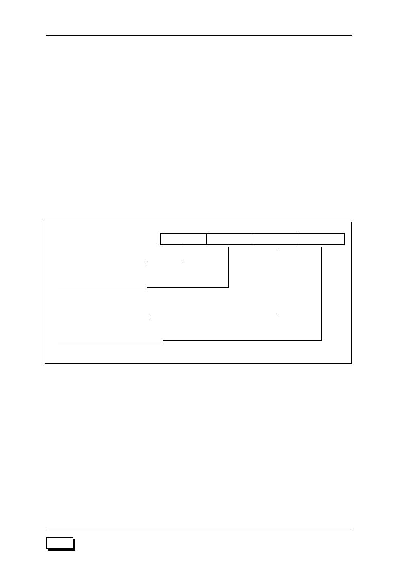
M193
6-6
ML63187/189B/193 User's Manual
Chapter 6 ML63193 Interrupt (INT193)
(3) Interrupt request registers (IRQ0 to IRQ4)
IRQ0, IRQ1, IRQ2, IRQ3 and IRQ4 are registers that consist of 4 bits each.
When an interrupt request is generated, the corresponding bit of the interrupt request register
is set to "1" in the first half of the S1 state of the next instruction. So that the CPU can receive
interrupt requests, set the master interrupt enable flag (MIE) to "1" and set the appropriate
flag of the corresponding interrupt enable register (IE0 to IE4) to "1".
The watchdog timer interrupt is non-maskable and does not depend upon the interrupt enable
register or the master interrupt enable register (MIEF).
Setting the appropriate bits of an interrupt request register to "1" allows software interrupts
to be generated.
When an interrupt request is received, the corresponding bits of IRQ0 to IRQ4 are cleared
to "0".
At system reset, each bit of IRQ0 through IRQ4 is initialized to "0".
bit 3: QXI1 (reQuest eXternal Interrupt 1)
The external interrupt 1 request flag.
The external interrupt 1 is assigned as the secondary function of each bit of port
C (PC.0 to PC.3). External interrupt 1 requests are generated by a 4-bit ORed input.
bit 2: QXI0 (reQuest eXternal Interrupt 0)
The external interrupt 0 request flag.
The external interrupt 0 is assigned as the secondary function of each bit of port
B (PB.0 to PB.3). External interrupt 0 requests are generated by a 4-bit ORed input.
QXI1
QXI0
QMD
QWDT
bit 3
bit 2
bit 1
bit 0
External interrupt 0 request flag
0: No request (initial value)
1: Request
Melody end interrupt request flag
0: No request (initial value)
1: Request
Watchdog timer interrupt request flag
0: No request (initial value)
1: Request
IRQ0 (055H)
(R/W)
External interrupt 1 request flag
0: No request (initial value)
1: Request
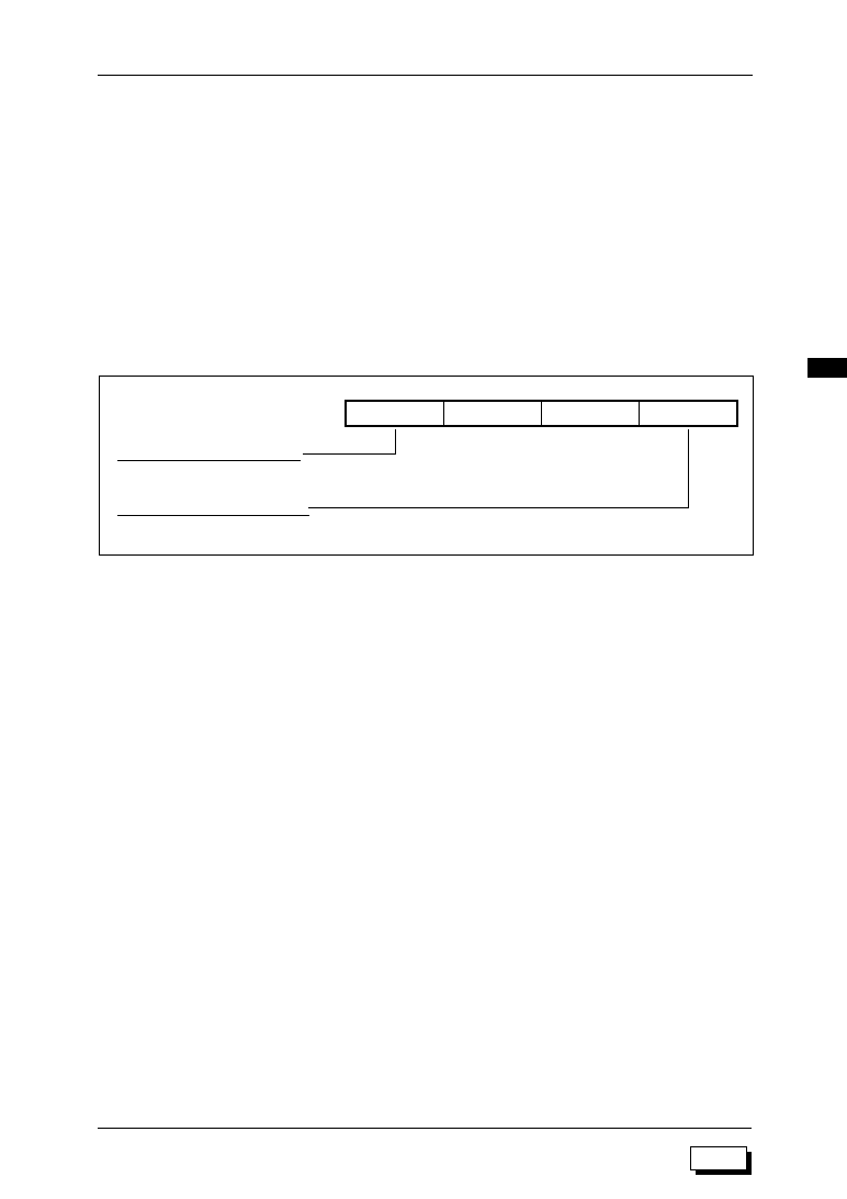
6-7
ML63187/189B/193 User's Manual
Chapter 6 ML63193 Interrupt (INT193)
6
M193
QXI5
--
--
QXI2
External interrupt 5 request flag
0: No request (initial value)
1: Request
bit 3
bit 2
bit 1
bit 0
IRQ1 (056H)
(R/W)
External interrupt 2 request flag
0: No request (initial value)
1: Request
bit 3: QXI5 (reQuest eXternal Interrupt 5)
External interrupt 5 request flag.
The external interrupt 5 is assigned as a secondary function to each bit (P0.0 to
0.3) of port 0.
An external interrupt request is generated through the 4-bit ORed input.
bit 0: QXI2 (reQuest eXternal Interrupt 2)
External interrupt 2 request flag.
The external interrupt 2 is assigned as a secondary function of port E.3 (PE.3).
Generation of the external interrupt 2 is triggered by the falling edge of the 128 Hz
or 4 kHz output of the time base counter.
bit 1: QMD (reQuest Melody Driver)
Melody end interrupt request flag.
Melody end interrupts are generated when the melody driver outputs the end note
data (END bit = "1").
bit 0: QWDT (reQuest WatchDog Timer)
Watchdog timer interrupt request flag.
When the watchdog timer is started and then overflow occurs, an interrupt is
requested. The watchdog timer interrupt is non-maskable and does not depend
upon the interrupt enable registers or the master interrupt enable register (MIE).

M193
6-8
ML63187/189B/193 User's Manual
Chapter 6 ML63193 Interrupt (INT193)
bit 3: QTM3 (reQuest TiMer 3)
Timer 3 interrupt request flag.
A timer 3 interrupt request is generated whenever timer 3 overflows.
bit 2: QTM2 (reQuest TiMer 2)
Timer 2 interrupt request flag.
A timer 2 interrupt request is generated whenever timer 2 overflows.
bit 1: QTM1 (reQuest TiMer 1)
Timer 1 interrupt request flag.
A timer 1 interrupt request is generated whenever timer 1 overflows.
bit 0: QTM0 (reQuest TiMer 0)
Timer 0 interrupt request flag.
A timer 0 interrupt request is generated whenever timer 0 overflows.
QTM3
QTM2
QTM1
QTM0
Timer 3 interrupt request flag
0: No request (initial value)
1: Request
bit 3
bit 2
bit 1
bit 0
Timer 2 interrupt request flag
0: No request (initial value)
1: Request
Timer 1 interrupt request flag
0: No request (initial value)
1: Request
Timer 0 interrupt request flag
0: No request (initial value)
1: Request
IRQ2 (057H)
(R/W)
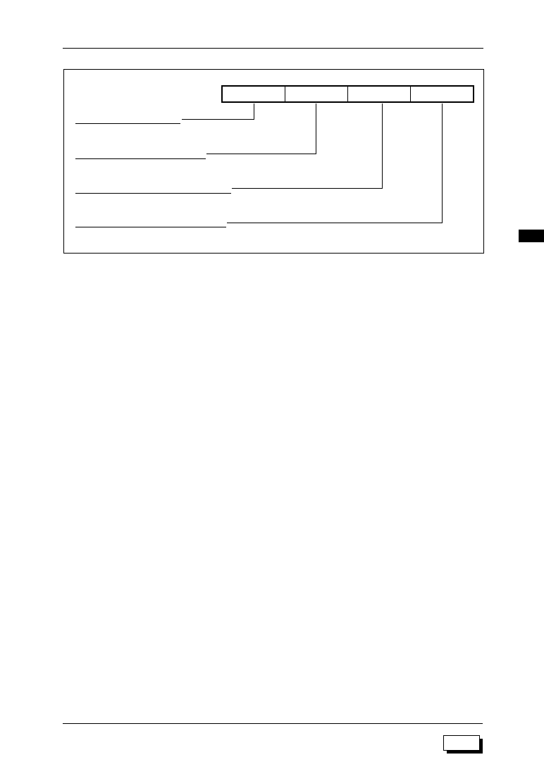
6-9
ML63187/189B/193 User's Manual
Chapter 6 ML63193 Interrupt (INT193)
6
M193
Q10Hz
QSFT
QST
QSR
10 Hz interrupt request flag
0: No request (initial value)
1: Request
bit 3
bit 2
bit 1
bit 0
IRQ3 (058H)
(R/W)
Shift register interrupt request flag
0: No request (initial value)
1: Request
Serial port transmit interrupt request flag
0: No request (initial value)
1: Request
Serial port receive interrupt request flag
0: No request (initial value)
1: Request
bit 3: Q10Hz (reQuest 10 Hz)
10 Hz interrupt request flag.
A 10 Hz interrupt request is generated whenever the 10 Hz carry generated by the
100 Hz timer counter is output.
bit 2: QSFT (reQuest ShiFT register)
Shift register interrupt request flag.
A shift register interrupt is generated when the 8-bit data transfer for the shift
register is completed.
bit 1: QST
Serial port transmit interrupt request flag.
A serial port ransmit interrupt request is generated when a serial port transmit
operation is completed.
bit 0: QSR
Serial port receive interrupt request flag.
A serial port receive interrupt is generated when a serial port receive operation is
completed.

M193
6-10
ML63187/189B/193 User's Manual
Chapter 6 ML63193 Interrupt (INT193)
Q2Hz
Q4Hz
Q16Hz
Q32Hz
2 Hz interrupt request flag
0: No request (initial value)
1: Request
bit 3
bit 2
bit 1
bit 0
4 Hz interrupt request flag
0: No request (initial value)
1: Request
16 Hz interrupt request flag
0: No request (initial value)
1: Request
32 Hz interrupt request flag
0: No request (initial value)
1: Request
IRQ4 (059H)
(R/W)
bit 3: Q2Hz (reQuest 2 Hz)
2 Hz interrupt request flag.
A 2 Hz interrupt request is generated at every falling edge of the 2 Hz output of the
time base counter.
bit 2: Q4Hz (reQuest 4 Hz)
4 Hz interrupt request flag.
A 4 Hz interrupt request is generated at every falling edge of the 4 Hz output of the
time base counter.
bit1: Q16Hz (reQuest 16 Hz)
16 Hz interrupt request flag.
A 16 Hz interrupt request is generated at every falling edge of the 16 Hz output of
the time base counter.
bit 0: Q32Hz (reQuest 32 Hz)
32 Hz interrupt request flag.
A 32 Hz interrupt request is generated at every falling edge of the 32 Hz output of
the time base counter.

6-11
ML63187/189B/193 User's Manual
Chapter 6 ML63193 Interrupt (INT193)
6
M193
6.3 Interrupt Sequence
6.3.1 Interrupt Processing
While MIE is "1", operation transfers to interrupt processing when individual interrupt factors
are generated.
The watchdog timer interrupt is non-maskable and regardless of the MIE flag status,
operation will shift to interrupt processing when the watchdog timer interrupt factor is
generated.
The following processes are performed when an interrupt is generated.
(1) MIE and the corresponding interrupt request flag are cleared to "0".
(2) The program counter (PC) is saved on the call stack.
(3) The call stack pointer (SP) is incremented by 1. (SP
®
SP+1)
(4) The starting address of the interrupt routine is loaded into the program counter (PC).
Interrupt processing is performed in 0 machine cycles.
Figure 6-2 shows the stack contents after an interrupt is generated.
PC11≠PC8
PC7≠PC4
PC3≠PC0
0H
1H
2H
3H
4H
0FH
SP position before interrupt
SP position after interrupt
13 12 11 10 9 8 7 6 5 4 3 2 1 0
PC13≠
PC12
Figure 6-2 Call Stack Contents after Interrupt Generation

M193
6-12
ML63187/189B/193 User's Manual
Chapter 6 ML63193 Interrupt (INT193)
6.3.2 Return from an Interrupt Routine
Return from a watchdog timer interrupt routine is performed with an "RTNMI" instruction.
Return from all other interrupt routines is performed with an "RTI" instruction.
Execution of "RTI" and "RTNMI" instructions both require 1 machine cycle.
When returning from an interrupt routine, the CPU performs the following processes.
(1) The call stack pointer (SP) is decremented by 1. (SP
®
SP≠1)
(2) MIE is set to "1" (when an "RTNMI" instruction is used, MIE is restored to its state prior
to the interrupt).
(3) 1 is added to the call stack contents and that value is loaded into the program counter (PC).
!
Notes:
∑
While the MIE flag is "0" (interrupt disabled state), if a watchdog timer interrupt is
processed and an "RTI" instruction is executed, the MIE flag will be set to "1" and interrupts
enabled.
∑
Use "RTNMI" instructions to return from watchdog timer interrupts only. Use "RTI"
instructions for normal interrupts.
6.3.3 Interrupt Hold Instructions
Interrupt requests are not received after execution of interrupt hold instruction.
The interrupt hold instructions follow.
∑
ROM table reference instructions
∑
Stack operation instructions
∑
Jump instructions
∑
Conditional branch instructions
∑
Call/return instructions
∑
"EI" (set MIE flag) instructions, "DI" (clear MIE flag) instructions and "MSA cadr15" (start
melody output) instructions within control instructions
!
Note:
If interrupt hold instructions are used consecutively, even if an interrupt is generated, that
interrupt may be put on hold for a considerable amount of time before the interrupt routine
begins. Interrupt requests are received after execution of an instruction other than interrupt
hold instructions.

M189B
M187
M193
Clock Generator Circuit (OSC)
Chapter 7
7


7-1
ML63187/189B/193 User's Manual
Chapter 7 Clock Generator Circuit (OSC)
7
M187
M189B
M193
Chapter 7 Clock Generator Circuit (OSC)
7.1 Overview
The clock generator circuit (OSC) consists of a low-speed clock generator circuit, a high-
speed clock generator circuit and a clock controller unit. The clock generator circuit generates
the system clock (CLK), time base clock (TBCCLK) and the high-speed clock (HSCLK).
The following modes can be selected for the low-speed clock generator circuit and the high-
speed clock generator circuit.
∑
Low-speed clock generator circuit: crystal oscillation mode or RC oscillation
mode (mask option selection)
∑
High-speed clock generator circuit: ceramic oscillation mode or RC oscillation
mode (software selection)
The system clock is the basic operation clock for the CPU. The time base clock is the basic
operation clock for the time base counter.
Depending on the contents of the frequency control register (FCON), the system clock
frequency is switched to either the output of the low-speed clock oscillation circuit (TBCCLK)
or the output of the high-speed clock oscillation circuit (HSCLK).
The frequency control register (FCON) also controls modes of the high-speed clock
oscillation circuit.
7.2 Clock Generator Circuit Configuration
Figure 7-1 shows a block diagram of the clock generator circuit.
Figure 7-1 Clock Generator Circuit Configuration
OSC1
External
circuit
OSC0
Oscillation enable
High-speed clock oscillation circuit
RC/ceramic oscillation select
High-speed clock output
V
DDH
XT0
External
circuit
XT1
Low-speed clock oscillation circuit
Low-speed clock output
V
DDL
TBCCLK
HSCLK
Time base clock
(TBCCLK)
System clock
(CLK)
High-speed clock
(HSCLK)
MPX
Clock select
control
FCON
3
3
FCON WRITE
Data bus

7-2
ML63187/189B/193 User's Manual
Chapter 7 Clock Generator Circuit (OSC)
M187
M189B
M193
7.3 Low-Speed Clock Generator Circuit
The low-speed clock generator circuit has two modes that are selected by the mask option,
the RC oscillation mode and crystal oscillation mode. The oscillation frequency is 30 to 80
kHz.
For the RC oscillation mode, attach an external resistor, R
OSL
, as shown in Figure 7-2(a).
For the crystal oscillation mode, attach an external crystal unit and capacitor, C
G
, as shown
in Figure 7-2(b).
Inside the IC
Low-speed clock
output
(a) External Circuit for RC Oscillation Mode
XT0
XT1
R
OSL
V
DDL
C
XT
V
SS
Inside the IC
Low-speed clock
output
(b) External Circuit for Crystal Oscillation Mode
XT0
XT1
Crystal
V
DDL
R
f
C
G
V
SS
V
SS
C
D
Figure 7-2 External Circuits for Low-Speed Clock Oscillation
!
Note:
For convenience, the descriptions of this manual assume that a 32.768 kHz crystal unit is
used in the low-speed clock oscillation circuit.
For the method of specifying mask options for the low-speed clock oscillation circuit, see
"Appendix G: Mask Option."

7-3
ML63187/189B/193 User's Manual
Chapter 7 Clock Generator Circuit (OSC)
7
M187
M189B
M193
Table 7-1 lists typical values of oscillation frequency when the low-speed side RC oscillation
mode is selected. Table 7-2 shows an example external component to be attached when the
low-speed side crystal oscillation mode is selected.
Table 7-1 Typical Oscillation Frequencies for the Low-Speed Side RC Oscillation Mode
Table 7-2 Example External Component for the Low-Speed Side Crystal Oscillation Mode
R
OSL
1.5 M
W
700 k
W
500 k
W
f
ROSL
32 kHz ±30%
60 kHz ±30%
80 kHz ±30%
C
G
12 pF
f
XT
32.768 kHz

7-4
ML63187/189B/193 User's Manual
Chapter 7 Clock Generator Circuit (OSC)
M187
M189B
M193
7.4 High-Speed Clock Generator Circuit
The high-speed clock generator circuit has two modes, the RC oscillation mode and ceramic
oscillation mode. Oscillation modes are set by OSCSEL (bit 2 of FCON). The maximum
oscillation frequency is 2 MHz.
∑
OSCSEL = "0" : RC oscillation mode
∑
OSCSEL = "1" : ceramic oscillation mode
If the high-speed clock is not to be used, leave the OSC0 and OSC1 pins open (unconnected).
For the RC oscillation mode, attach an external resistor, R
OSH
, as shown in Figure 7-3(a).
For the ceramic oscillation mode, attach an external ceramic unit and capacitors as shown
in Figure 7-3(b).
(a) External Circuit for RC Oscillation Mode
OSC1
OSC0
(b) External Circuit for Ceramic Oscillation Mode
V
DDH
V
DDH
R
OSH
High-speed
clock output
High-speed
clock output
Oscillation
enable
V
SS
C
L1
C
L0
V
DDH
V
DDH
Oscillation enable
Ceramic resonator
OSC1
OSC0
C
OS
Figure 7-3 External Circuits for High-Speed Clock Oscillation

7-5
ML63187/189B/193 User's Manual
Chapter 7 Clock Generator Circuit (OSC)
7
M187
M189B
M193
Table 7-3 lists typical values of oscillation frequency when the high-speed side RC oscillation
mode is selected. Table 7-4 lists example external components to be attached when the high-
speed side ceramic oscillation mode is selected.
Table 7-3 Typical Oscillation Frequencies for the High-Speed Side RC Oscillation Mode
Table 7-4 Example External Components for the High-Speed Side Ceramic Oscillation Mode
* Ceramic unit manufactured by Murata MFG. Co., Ltd.
R
OSH
(k
W)
V
DD
(V)
Backup flag
f
ROSH
400
1.5
200 kHz ±30%
75
ON
1 MHz ±30%
100
700 kHz ±30%
75
3.0
OFF
1 MHz ±30%
51
1.35 MHz ±30%
30
2 MHz ±30%
100
700 kHz ±30%
C
L0
(pF)
C
L1
(pF)
330
330
150
150
68
68
30
30
220
220
Ceramic unit
CSB200D (200 kHz)*
CSB300D (300 kHz)*
CSB500E (500 kHz)*
CSB1000J (1 MHz)*
CSA2.00MG (2 MHz)*

7-6
ML63187/189B/193 User's Manual
Chapter 7 Clock Generator Circuit (OSC)
M187
M189B
M193
7.5 System Clock Control
The system clock is the basic operation clock of the CPU.
The clock can be selected as follows with the CPUCLK (bit 0 of FCON) setting.
∑
CPUCLK = "0" (initial value)
The output of the low-speed clock generator circuit (TBCCLK) is the system
clock.
∑
CPUCLK = "1"
The output of the high-speed clock generator circuit (HSCLK) is the system
clock.
When HSCLK is selected as the system clock, the high-speed clock must be in the oscillating
state (ENOSC = "1"). The crystal generator circuit will continue to oscillate even when the
high-speed generator circuit is selected.
To reduce the total power consumption in applications that use the high-speed clock
generator circuit, the following clock controls are generally implemented in software.
∑
During normal operation, the output of the low-speed clock generator circuit (CPUCLK =
"0") should be the system clock.
∑
Only when high-speed operation is necessary should the high-speed clock oscillate
(ENOSC = "1") and output of the high-speed clock generator circuit (CPUCLK = "1")
should be selected.
For details of the system clock select timing, refer to section 7.7, "System Clock Select
Timing."

7-7
ML63187/189B/193 User's Manual
Chapter 7 Clock Generator Circuit (OSC)
7
M187
M189B
M193
7.6 Frequency Control Register (FCON)
FCON is a special function register (SFR) that selects the system clock.
--
OSCSEL
ENOSC
CPUCLK
RC oscillation/ceramic oscillation mode select
0: RC oscillation mode (initial value)
1: Ceramic oscillation mode
High-speed clock oscillation start/stop select
0: Oscillation stop (initial value)
1: Oscillation start
System clock select
0: Low-speed clock oscillation output (initial value)
1: High-speed clock oscillation output
FCON (062H)
(R/W)
bit 3
bit 2
bit 1
bit 0
bit 2: OSCSEL
This bit selects the RC oscillation mode or the ceramic oscillation mode of the high-
speed clock generator circuit. At system reset, this bit is cleared to "0", selecting
the RC oscillation mode.
bit 1: ENOSC
This bit starts and stops oscillation of the high-speed clock generator circuit. At
system reset, this bit is cleared to "0", stopping oscillation of the high-speed clock
generator circuit.
bit 0: CPUCLK
This bit selects the system clock, the basic operation clock of the CPU. At system
reset, this bit is cleared to "0", selecting output of the low-speed clock generator
circuit (TBCCLK).
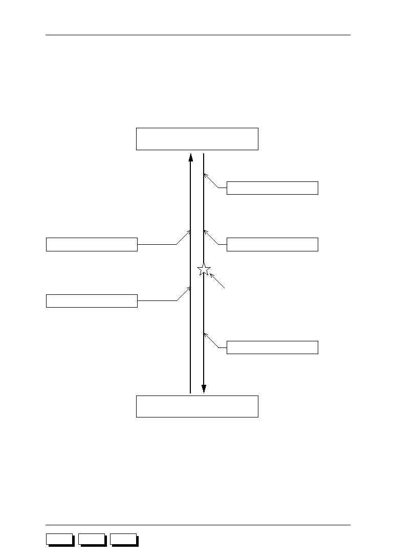
7-8
ML63187/189B/193 User's Manual
Chapter 7 Clock Generator Circuit (OSC)
M187
M189B
M193
7.7 System Clock Select Timing
After system reset, the system clock is TBCCLK.
When high-speed operation is necessary, switch the system clock to HSCLK.
A flowchart of system clock operation is shown below.
TBCCLK
(Low-speed clock generator circuit output)
System clock status
HSCLK
(High-speed clock generator circuit output)
After system reset, the low-
speed clock generator output
is the system clock.
OSCSEL (bit 2 of FCON) setting
(1) High-speed clock oscillation mode select
OSCSEL = "0" : RC oscillation mode
(initial value)
OSCSEL = "1" : Ceramic oscillation mode
ENOSC (bit 1 of FCON) = "0"
(2) High-speed clock oscillation stop
ENOSC = "0" : Stop high-speed clock oscillation
(initial value)
ENOSC = "1" : Start high-speed clock oscillation
Software processing
Software processing
ENOSC (bit 1 of FCON) = "1"
(2) High-speed clock oscillation start
ENOSC = "0" : Stop high-speed clock oscillation
(initial value)
ENOSC = "1" : Start high-speed clock oscillation
Wait:
When RC oscillation mode selected:
300
ms or more
When ceramic oscillation mode selected:
10 ms or more
CPUCLK (bit 0 of FCON) = "1"
(3) High-speed clock oscillation output select
CPUCLK = "0" : Low-speed clock oscillation output
(initial value)
CPUCLK = "1" : High-speed clock oscillation output
CPUCLK (bit 0 of FCON) = "0"
(1) Low-speed clock oscillation output select
CPUCLK = "0" : Low-speed clock oscillation output
(initial value)
CPUCLK = "1" : High-speed clock oscillation output
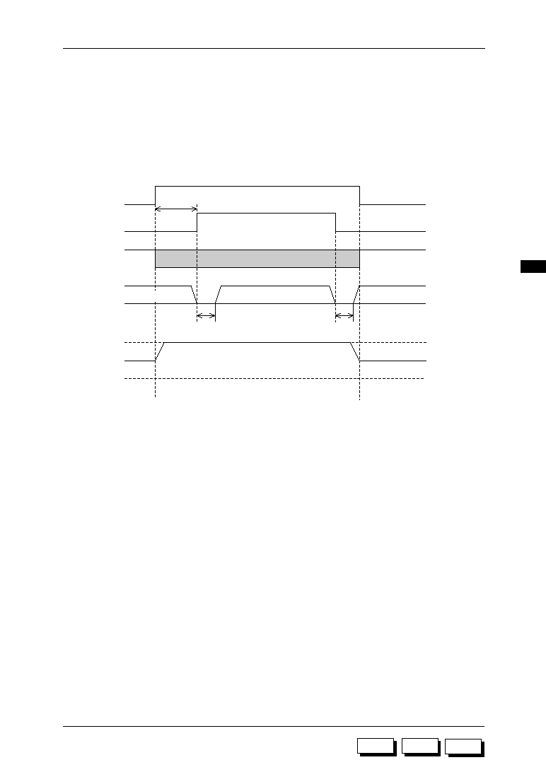
7-9
ML63187/189B/193 User's Manual
Chapter 7 Clock Generator Circuit (OSC)
7
M187
M189B
M193
When ENOSC (bit 1 of FCON) is set to "1", oscillation starts in the mode selected by OSCSEL.
At the same time, the internal logic power supply (V
DDL
) switches from the constant voltage
circuit output level (approx. 1.5 V) to the V
DDH
level. Next, if CPUCLK is set to "1", the system
clock switches from crystal oscillation output (TBCCLK) to high-speed clock output (HSCLK).
Figure 7-4 shows the system clock select timing and status of the internal logic power supply
(V
DDL
).
ENOSC
CPUCLK
OSC1
System clock
T
WAIT
High-speed clock
Low-speed clock
0.5 to 1.0 high-speed clocks
0.5 to 1.0 low-speed clocks
V
DDL
Internal logic
power supply
V
DDH
V
SS
= 0 V
Approx. 1.5 V
(typ.)
Low-speed clock
Figure 7-4 System Clock Select Timing
In the ceramic oscillation mode, 10 ms are required from the time when ENOSC is set to "1"
until the high-speed clock generator circuit enters the oscillating state. Therefore, in this
mode, when switching CPUCLK to a high-speed setting, wait for an interval of at least T
WAIT
= 10 ms after the rising edge of ENOSC.
In the CR oscillation mode, oscillation begins soon after setting ENOSC to "1". When
switching CPUCLK to a high-speed setting, wait for an interval of at least T
WAIT
= 300
m
s after
the rising edge of ENOSC.
When switching from the high-speed mode to the low-speed mode, set the CPUCLK bit to "0",
and sometime after the next instruction, set the ENOSC bit to "0".
For details regarding the constant voltage circuit for the internal logic power supply, refer to
Chapter 19, "Backup Circuit."

7-10
ML63187/189B/193 User's Manual
Chapter 7 Clock Generator Circuit (OSC)
M187
M189B
M193

M189B
M187
M193
Time Base Counter (TBC)
Chapter 8
8


8-1
ML63187/189B/193 User's Manual
Chapter 8 Time Base Counter (TBC)
8
M187
M189B
M193
Chapter 8 Time Base Counter (TBC)
8.1 Overview
The time base counter (TBC) is a 15-bit internal counter, which generates the clock supplied
to internal peripheral functions.
The TBC clock is a time base clock (TBCCLK).
TBC outputs are used for functions such as time base interrupts and various other circuits.
TBC8≠11 and TBC12≠15 can be read/reset by software.
The TBC generates an interrupt request at the falling edge of 32 Hz/16 Hz/4 Hz/2 Hz output.
The TBC is initialized to 0000H at system reset.
8.2 Time Base Counter Configuration
The configuration of the time base counter (TBC) is shown in Figure 8-1.
bit 3
bit 2
bit 1
bit 0
bit 3
bit 2
bit 1
bit 0
1 Hz
2 Hz
4 Hz
8 Hz
16 Hz
32 Hz
64 Hz
128 Hz
256 Hz
512 Hz
1 kHz
2 kHz
4 kHz
8 kHz
16 kHz
(1 Hz)
(2 Hz)
(4 Hz)
(8 Hz)
(16 Hz)
(32 Hz)
(64 Hz)
(128 Hz)
(256 Hz)
(512 Hz)
(1 kHz)
(2 kHz)
(4 kHz)
(8 kHz)
(16 kHz)
TBC7
TBC6
TBC5
TBC4
TBC3
TBC2
TBC1
TBC11
TBC10
TBC9
TBC8
TBC15
TBC14
TBC13
TBC12
R
R
R
TBCR0 READ
TBCR1 READ
TBCR1 WRITE
TBCR0 WRITE
RESET0
Data bus
TBCCLK
(32.768 kHz)
2HzINT
4HzINT
16HzINT
32HzINT
(1/32768TBC)
(1/16384TBC)
(1/8192TBC)
(1/4096TBC)
(1/2048TBC)
(1/1024TBC)
(1/512TBC)
(1/256TBC)
(1/128TBC)
(1/64TBC)
(1/32TBC)
(1/16TBC)
(1/8TBC)
(1/4TBC)
(1/2TBC)
Figure 8-1 Time Base Counter (TBC) Configuration
(when a 32.768 kHz crystal is used for low-speed clock oscillation)

8-2
ML63187/189B/193 User's Manual
Chapter 8 Time Base Counter (TBC)
M187
M189B
M193
8.4 Time Base Counter Operation
After system reset the time base counter (TBC) begins to count up from 0000H. The count
is incremented at the falling edge of the TBCCLK.
TBC 32 Hz/16 Hz/4 Hz/2 Hz outputs are used as time base interrupts. At each output falling
edge, four bits of interrupt request register 4 (IRQ4) are set to "1", namely bit 3 (Q32Hz), bit
2 (Q16Hz), bit 1 (Q4Hz) and bit 0 (Q2Hz), requesting an interrupt to the CPU. TBC outputs
are also used as clocks for various circuits.
TBC 1 to 8 Hz output and 16 to 128 Hz output can be read through the time base counter
register 0/1 (TBCR0/TBCR1).
A write operation to TBCR1 sets the 1 to 8 Hz output counter to "0", and a write operation to
TBCR0 sets both the 1 to 8 Hz and 16 to 128 Hz output counters to "0". The write data in these
write operations has no significance. For example, the "MOV TBCR0, A" instruction can be
used to write, but is not dependent on accumulator content in any way. When write is executed
to TBCR0 and TBCR1 and the 1 to 8 Hz and 16 to 128 Hz counters reset, interrupt requests
are generated if 32 Hz/16 Hz/4 Hz/2 Hz outputs have been set to "1". To disable these
interrupts, first set the master interrupt enable flag (MIE) or interrupt enable register 4 (IE4)
to "0", execute the write operation to TBCR 0/1, and set the interrupt request flag 4 (IRQ4)
to "0".
Figure 8-2 shows interrupt generation timing and time base counter output reset timing by
writing "1" to TBCR0 and TBCR1.
8.3 Time Base Counter Registers
Time base counter register 0 (TBCR0), time base counter register 1 (TBCR1)
These 4-bit special function registers (SFRs) are used to read the 1 to 8 Hz and 16 to 128 Hz
outputs of the time base counter.
A write operation to TBCR0 sets both the 1 to 8 Hz and 16 to 128 Hz outputs to "0", and a write
operation to TBCR1 sets the 1 to 8 Hz output to "0".
16 Hz
32 Hz
64 Hz
128 Hz
TBCR0 (060H)
(R/W)
bit 3
bit 2
bit 1
bit 0
1 Hz
2 Hz
4 Hz
8 Hz
TBCR1 (061H)
(R/W)
bit 3
bit 2
bit 1
bit 0

8-3
ML63187/189B/193 User's Manual
Chapter 8 Time Base Counter (TBC)
8
M187
M189B
M193
Figure 8-2 Interrupt Timing and Reset Timing by Writing "1" to TBCR0, TBCR1
Write
TBCR0
256 Hz
128 Hz
64 Hz
32 Hz
16 Hz
Write
TBCR1
16 Hz
8 Hz
4 Hz
2 Hz
1 Hz
1 second
+0
≠1/16
1 second
+0
≠1/256
Shows interrupt timing

8-4
ML63187/189B/193 User's Manual
Chapter 8 Time Base Counter (TBC)
M187
M189B
M193
M189B
M187
M193
Chapter 9
9
Timers (TIMER)


9-1
ML63187/189B/193 User's Manual
Chapter 9 Timers (TIMER)
9
M187
M189B
M193
Chapter 9 Timers (TIMER)
9.1 Overview
The ML63187, ML63189B, and ML63193 have four internal 8-bit timers (0 to 3). Timers 0 and
1, or timers 2 and 3, can be used in tandem as a 16-bit timer.
Timers 0 and 1 have three operation modes: auto-reload mode, capture mode and frequency
measurement mode. Timers 2 and 3 have two modes: auto-reload and frequency measure-
ment. Timer clock may be set to the time base clock (TBCCLK: 32.768 kHz), the high-speed
clock (HSCLK), or an external clock. When using the timers as a 16-bit timer, the overflow
signals of timers 0 and 2 are used as the clocks for timers 1 and 3, respectively.
Timers can be used not only for pulse generation and time measurement, but as baud rate
generators for serial communication in the ML63193.
Figure 9-1 Timer 0 Configuration
9.2 Timer Configuration
Figures 9-1 through 9-4 show the configuration of timers 0 to 3.
Control
circuit
Frequency
measurement
control circuit
Capture
control circuit
TM0CL
TM0CH
TM0DL
TM0DH
8
8
Capture
Reload
4
4
4
4
D
Q
D
Q
Q
R
TM0CK
TM0 overflow
TM0INT
PB.0/TM0OVF
Data bus
TBCCLK
HSCLK
PB.2/T02CK
64 Hz
437C
PB.0/TM0CAP
TM0CAP
TM0CK
RESETS
OV
16 kHz
8 kHz
4 kHz
2 kHz
1 kHz
512 Hz
256 Hz
128 Hz
64 Hz
437C
16-bit timer
(Timer 0 overflow signal is
used as clock for timer 1)
Clock
TBCCLK / HSCLK / External clock (T02CK, T13CK)
Auto-reload mode
Capture mode
(Timer 2 overflow signal is
used as clock for timer 3)
--
8-bit timer
Timer 0
Timer 2
Timer 1
Timer 3
--
Frequency measurement mode
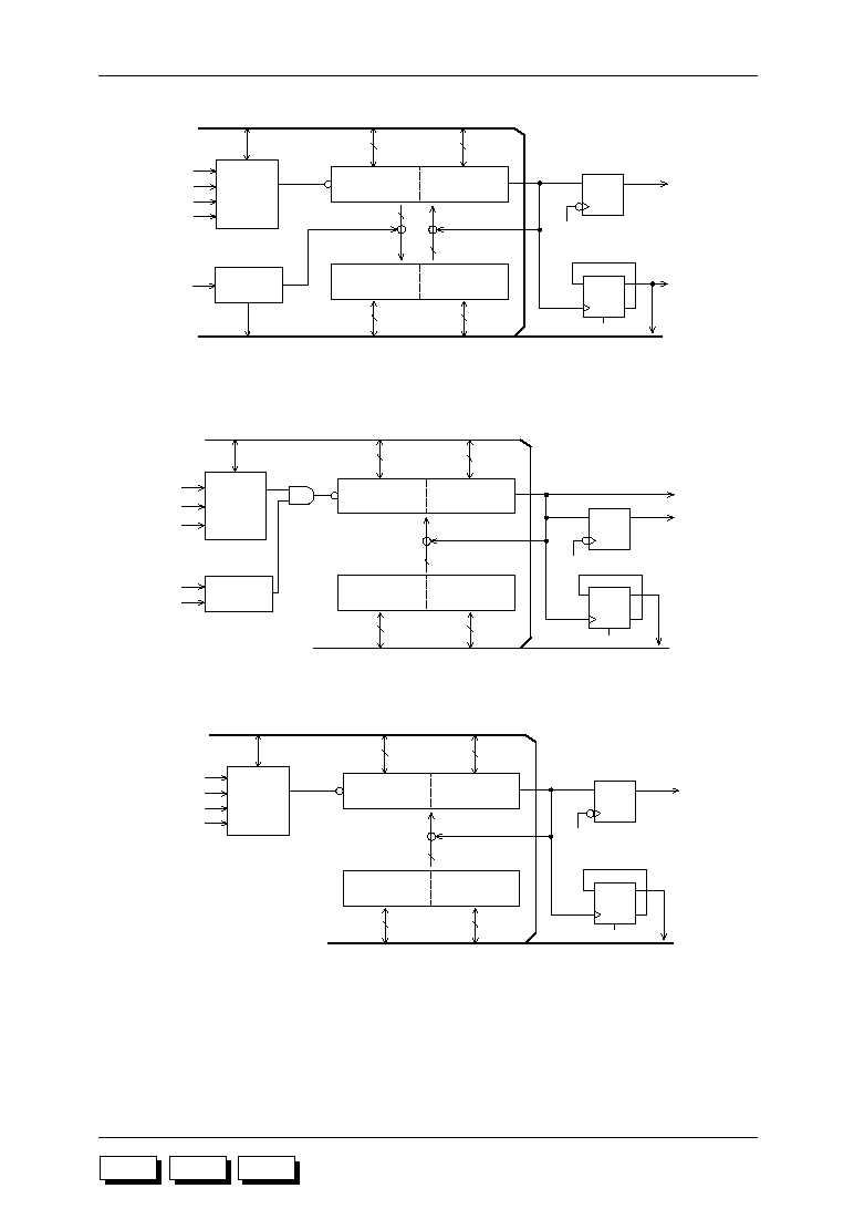
9-2
ML63187/189B/193 User's Manual
Chapter 9 Timers (TIMER)
M187
M189B
M193
Control
circuit
Capture
control circuit
TM1CL
TM1CH
TM1DL
TM1DH
8
8
Capture
Reload
4
4
4
4
D
Q
Q
R
D
Q
TM1CK
TM1INT
PB.1/TM1OVF
Data bus
TBCCLK
HSCLK
PB.3/T13CK
PB.1/TM1CAP
TM1CAP
TM1CK
RESETS
TM0 overflow
OV
TM1
overflow
Figure 9-2 Timer 1 Configuration
Control
circuit
Frequency
measurement
control circuit
TM2CL
TM2CH
TM2DL
TM2DH
8
Reload
4
4
4
4
D
Q
D
Q
Q
R
TM2CK
TM2 overflow
TM2INT
TM2OVF
Data bus
TBCCLK
HSCLK
PB.2/T02CLK
64 Hz
437C
TM2CK
RESETS
OV
Figure 9-3 Timer 2 Configuration
Control
circuit
TM3CL
TM3CH
TM3DL
TM3DH
8
Reload
4
4
4
4
D
Q
Q
R
D
Q
TM3CK
TM3INT
Data bus
TBCCLK
HSCLK
PB.3/T13CK
TM3CK
RESETS
TM2 overflow
OV
TM3OVF
Figure 9-4 Timer 3 Configuration
9-3
ML63187/189B/193 User's Manual
Chapter 9 Timers (TIMER)
9
M187
M189B
M193
9.3 Timer Registers
The following four registers are used for timer control.
(1) Timer data registers
(TM0DL, TM0DH, TM1DL, TM1DH, TM2DL, TM2DH, TM3DL, TM3DH)
(2) Timer counter registers
(TM0CL, TM0CH, TM1CL, TM1CH, TM2CL, TM2CH, TM3CL, TM3CH)
(3) Timer control registers
(TM0CON0, TM0CON1, TM1CON0, TM1CON1, TM2CON0, TM2CON1, TM3CON0,
TM3CON1)
(4) Timer status registers
(TM0STAT, TM1STAT, TM2STAT, TM3STAT)
Each register is described below.
(1) Timer data registers
(TM0DL, TM0DH, TM1DL, TM1DH, TM2DL, TM2DH, TM3DL, TM3DH)
∑
During the auto-reload mode, timer data registers store the reload values.
∑
During the capture mode, timer data registers store the capture data.
Writing to a timer data register causes the contents of the timer counter register
to be transferred to the timer data register.
∑
At system reset, all valid bits are cleared to "0".
∑
Note regarding register values:
Writing to the timer counter register causes the same value to also be written to
the timer data register. However, when writing to the timer data register, the
same value is not written to the timer counter register.
Timer 0 Registers
T0D3
T0D2
T0D1
T0D0
(068H)
(R/W)
TM0DL
(Timer 0 lower)
bit 3
bit 2
bit 1
bit 0
T0D7
T0D6
T0D5
T0D4
(069H)
(R/W)
TM0DH
(Timer 0 upper)
bit 3
bit 2
bit 1
bit 0
Timer 1 Registers
T1D3
T1D2
T1D1
T1D0
(06AH)
(R/W)
TM1DL
(Timer 1 lower)
bit 3
bit 2
bit 1
bit 0
T1D7
T1D6
T1D5
T1D4
(06BH)
(R/W)
TM1DH
(Timer 1 upper)
bit 3
bit 2
bit 1
bit 0
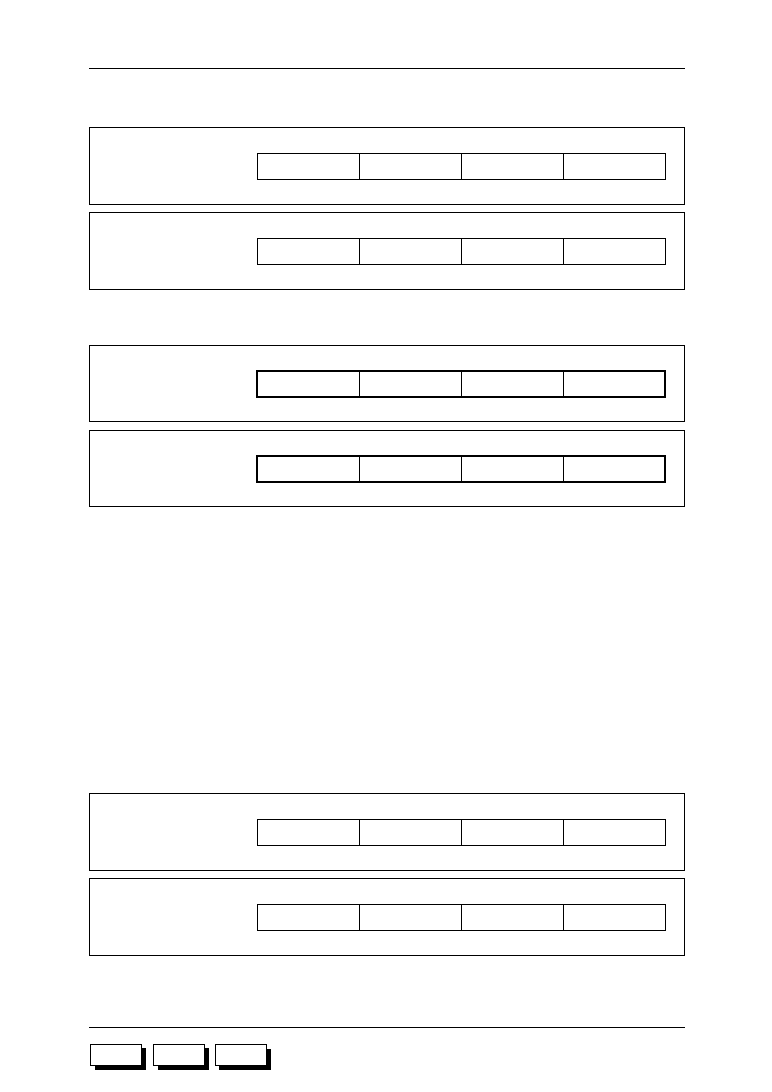
9-4
ML63187/189B/193 User's Manual
Chapter 9 Timers (TIMER)
M187
M189B
M193
Timer 2 Registers
T2D3
T2D2
T2D1
T2D0
(076H)
(R/W)
TM2DL
(Timer 2 lower)
bit 3
bit 2
bit 1
bit 0
T2D7
T2D6
T2D5
T2D4
(077H)
(R/W)
TM2DH
(Timer 2 upper)
bit 3
bit 2
bit 1
bit 0
Timer 3 Registers
T3D3
T3D2
T3D1
T3D0
(078H)
(R/W)
TM3DL
(Timer 3 lower)
bit 3
bit 2
bit 1
bit 0
T3D7
T3D6
T3D5
T3D4
(079H)
(R/W)
TM3DH
(Timer 3 upper)
bit 3
bit 2
bit 1
bit 0
(2) Timer counter registers
(TM0CL, TM0CH, TM1CL, TM1CH, TM2CL, TM2CH, TM3CL, TM3CH)
∑
8-bit binary counter operation
∑
At system reset, all valid bits are cleared to "0".
∑
Note regarding register values:
Writing to the timer counter register causes the same value to also be written to
the timer data register. However, when writing to the timer data register, the
same value is not written to the timer counter register.
Timer 0 Registers
T0C3
T0C2
T0C1
T0C0
(06CH)
(R/W)
TM0CL
(Timer 0 lower)
bit 3
bit 2
bit 1
bit 0
T0C7
T0C6
T0C5
T0C4
(06DH)
(R/W)
TM0CH
(Timer 0 upper)
bit 3
bit 2
bit 1
bit 0
9-5
ML63187/189B/193 User's Manual
Chapter 9 Timers (TIMER)
9
M187
M189B
M193
Timer 1 Registers
T1C3
T1C2
T1C1
T1C0
(06EH)
(R/W)
TM1CL
(Timer 1 lower)
bit 3
bit 2
bit 1
bit 0
T1C7
T1C6
T1C5
T1C4
(06FH)
(R/W)
TM1CH
(Timer 1 upper)
bit 3
bit 2
bit 1
bit 0
Timer 2 Registers
T2C3
T2C2
T2C1
T2C0
(07AH)
(R/W)
TM2CL
(Timer 2 lower)
bit 3
bit 2
bit 1
bit 0
T2C7
T2C6
T2C5
T2C4
(07BH)
(R/W)
TM2CH
(Timer 2 upper)
bit 3
bit 2
bit 1
bit 0
Timer 3 Registers
T3C3
T3C2
T3C1
T3C0
(07CH)
(R/W)
TM3CL
(Timer 3 lower)
bit 3
bit 2
bit 1
bit 0
T3C7
T3C6
T3C5
T3C4
(07DH)
(R/W)
TM3CH
(Timer 3 upper)
bit 3
bit 2
bit 1
bit 0
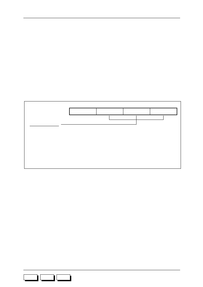
9-6
ML63187/189B/193 User's Manual
Chapter 9 Timers (TIMER)
M187
M189B
M193
(3) Timer control registers
(TM0CON0, TM0CON1, TM1CON0, TM1CON1, TM2CON0, TM2CON1, TM3CON0,
TM3CON1)
∑
Timer control registers select the operation mode and clock for each timer.
∑
At system reset, all valid bits are cleared to "0".
∑
Note regarding register values:
Writing to the timer counter register causes the same value to also be written to
the timer data register. However, when writing to the timer data register, the
same value is not written to the timer counter register.
Timer 0 Registers
To use timer 1 in combination as a 16-bit timer, set timer 1 control registers TM1CON0 and
TM1CON1.
--
FMEAS0
TM0ECAP
TM0RUN
TM0CON0 (070H)
(R/W)
bit 3
bit 2
bit 1
bit 0
Timer 0 mode select
bit 2
0
0
0
0
1
1
1
1
bit 1
0
0
1
1
0
0
1
1
bit 0
0
1
0
1
0
1
0
1
: Auto-reload mode stop (initial value)
: Auto-reload mode operation
: Capture mode stop
: Capture mode operation
: Frequency measurement mode operation
: Not used
: Not used
: Not used
bit 2, 1, 0: FMEAS0, TM0ECAP, TM0RUN
These bits select the timer 0 operation mode.
The timer 0 operation mode can be selected as auto-reload mode, capture mode,
or frequency measurement mode.
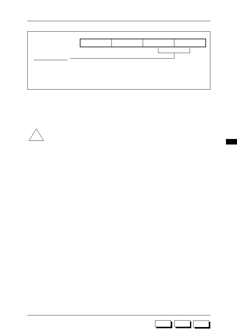
9-7
ML63187/189B/193 User's Manual
Chapter 9 Timers (TIMER)
9
M187
M189B
M193
--
--
TM0CL1
TM0CL0
TM0CON1 (071H)
(R/W)
bit 3
bit 2
bit 1
bit 0
Timer 0 clock select
bit 1
0
0
1
1
bit 0
0
1
0
1
: TBCCLK (initial value)
: HSCLK (high-speed clock)
: External clock
: Not used
bit 1, 0: TM0CL1, TM0CL0
These bits select the timer 0 clock.
The timer 0 clock can be selected as TBCCLK (low-speed clock), HSCLK (high-
speed clock), or external clock (T02CK: secondary function of PB.2).
!
Note:
If HSCLK is used as the clock, after ENOSC (bit 1 of FCON) is set to "1", wait for the following
time interval before starting timer operation.
∑
Wait at least 10 ms when using ceramic oscillation.
∑
Wait at least 300
m
s when using RC oscillation.

9-8
ML63187/189B/193 User's Manual
Chapter 9 Timers (TIMER)
M187
M189B
M193
Timer 1 Registers
--
--
TM1ECAP
TM1RUN
TM1CON0 (072H)
(R/W)
bit 3
bit 2
bit 1
bit 0
Timer 1 mode select
bit 1
0
0
1
1
bit 0
0
1
0
1
: Auto-reload mode stop or 16-bit timer mode (initial value)
: Auto-reload mode operation
: Capture mode stop
: Capture mode operation
bit 1, 0: TM1ECAP, TM1RUN
These bits select the timer 1 operation mode.
The timer 1 operation mode can be selected as auto-reload mode, capture mode,
or 16-bit timer mode.
--
--
TM1CL1
TM1CL0
TM1CON1 (073H)
(R/W)
bit 3
bit 2
bit 1
bit 0
Timer 1 clock select
bit 1
0
0
1
1
bit 0
0
1
0
1
: TBCCLK (initial value)
: HSCLK
: External clock
: Timer 0 overflow (16-bit timer mode)
bit 1, 0: TM1CL1, TM1CL0
These bits select the timer 1 clock.
The timer 1 clock can be selected as TBCCLK (low-speed clock), HSCLK (high-
speed clock), external clock (T13CK: secondary function of PB.2), or the timer 0
overflow flag.
When using as a 16-bit timer, select timer 0 overflow for the clock.
!
Note:
If HSCLK is used as the clock, after ENOSC (bit 1 of FCON) is set to "1", wait for the following
time interval before starting timer operation.
∑
Wait at least 10 ms when using ceramic oscillation.
∑
Wait at least 300
m
s when using RC oscillation.
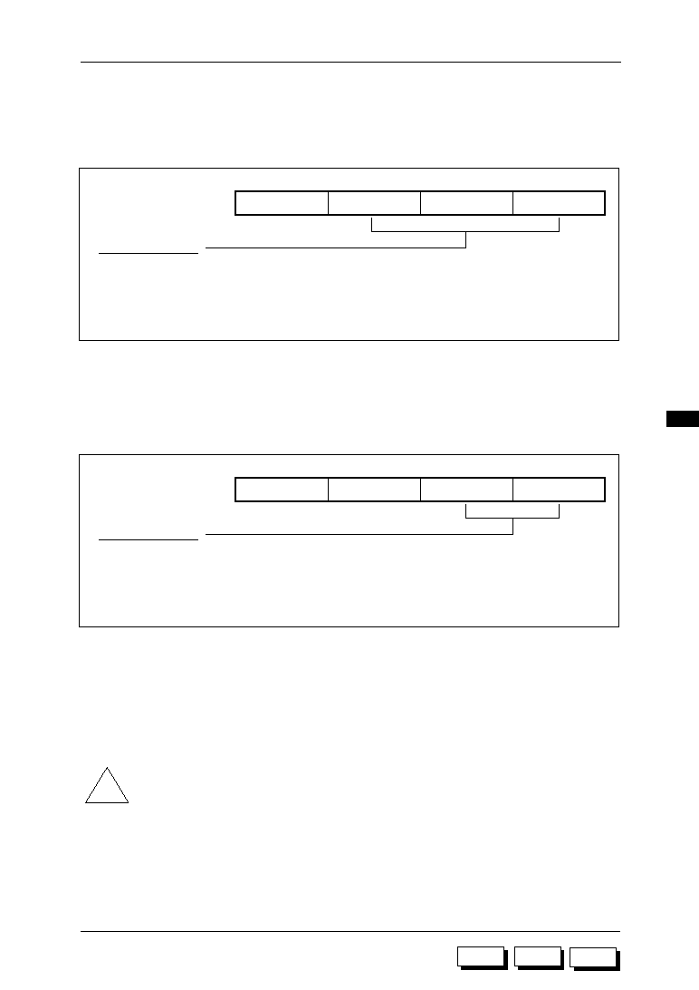
9-9
ML63187/189B/193 User's Manual
Chapter 9 Timers (TIMER)
9
M187
M189B
M193
Timer 2 Registers
To use timer 3 in combination as a 16-bit timer, set timer 3 control registers TM3CON0 and
TM3CON1.
--
FMEAS2
--
TM2RUN
TM2CON0 (07EH)
(R/W)
bit 3
bit 2
bit 1
bit 0
Timer 2 mode select
bit 2
0
0
1
1
bit 0
0
1
0
1
: Auto-reload mode stop (initial value)
: Auto-reload mode operation
: Frequency measurement mode operation
: Not used
bit 2, 0: FMEAS2, TM2RUN
These bits select the timer 2 operation mode.
The timer 2 operation mode can be selected as auto-reload mode or frequency
measurement mode.
--
--
TM2CL1
TM2CL0
TM2CON1 (07FH)
(R/W)
bit 3
bit 2
bit 1
bit 0
Timer 2 clock select
bit 1
0
0
1
1
bit 0
0
1
0
1
: TBCCLK (initial value)
: HSCLK
: External clock
: Not used
bit 1, 0: TM2CL1, TM2CL0
These bits select the timer 2 clock.
The timer 2 clock can be selected as TBCCLK (low-speed clock), HSCLK (high-
speed clock), or external clock (T02CK: secondary function of PB.2).
!
Note:
If HSCLK is used as the clock, after ENOSC (bit 1 of FCON) is set to "1", wait for the following
time interval before starting timer operation.
∑
Wait at least 10 ms when using ceramic oscillation.
∑
Wait at least 300
m
s when using RC oscillation.

9-10
ML63187/189B/193 User's Manual
Chapter 9 Timers (TIMER)
M187
M189B
M193
Timer 3 Registers
--
--
--
TM3RUN
TM3CON0 (080H)
(R/W)
bit 3
bit 2
bit 1
bit 0
Timer 3 mode select
0 : Auto-reload mode stop or 16-bit timer mode (initial value)
1 : Auto-reload mode operation
bit 0: TM3RUN
This bit selects the timer 3 operation mode.
The timer 3 operation mode can be selected as auto-reload mode or 16-bit timer
mode.
--
--
TM3CL1
TM3CL0
TM3CON1 (081H)
(R/W)
bit 3
bit 2
bit 1
bit 0
Timer 3 clock select
bit 1
0
0
1
1
bit 0
0
1
0
1
: TBCCLK (initial value)
: HSCLK
: External clock
: Timer 2 overflow (16-bit timer mode)
bit 1, 0: TM3CL1, TM3CL0
These bits select the timer 3 clock.
The timer 3 clock can be selected as TBCCLK (low-speed clock), HSCLK (high-
speed clock), external clock (T13CK: secondary function of PB.3), or the timer 2
overflow flag.
When using as a 16-bit timer, select timer 2 overflow for the clock.
!
Note:
If HSCLK is used as the clock, after ENOSC (bit 1 of FCON) is set to "1", wait for the following
time interval before starting timer operation.
∑
Wait at least 10 ms when using ceramic oscillation.
∑
Wait at least 300
m
s when using RC oscillation.
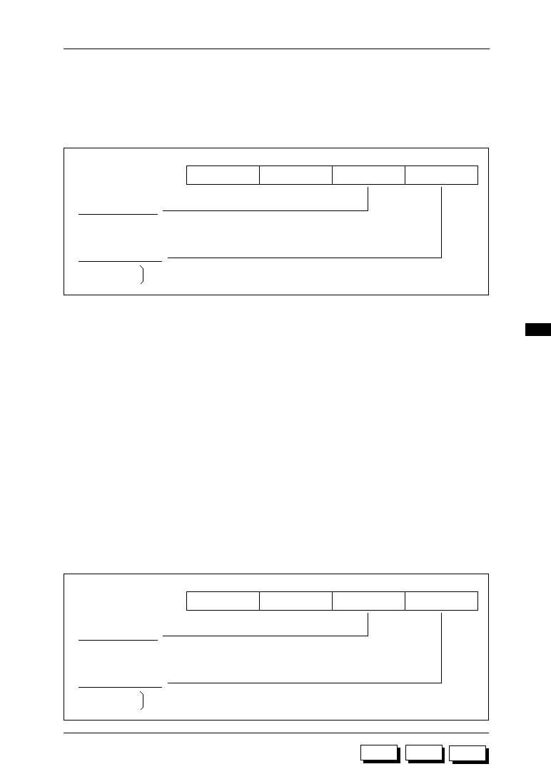
9-11
ML63187/189B/193 User's Manual
Chapter 9 Timers (TIMER)
9
M187
M189B
M193
(4) Timer status registers (TM0STAT, TM1STAT, TM2STAT, TM3STAT)
∑
Timer status registers read the status of each timer.
∑
At system reset, all valid bits are cleared to "0".
Timer 0 Registers
--
--
TM0CAP
TM0OVF
TM0STAT (074H)
(R)
bit 3
bit 2
bit 1
bit 0
Timer 0 capture flag
0: No new capture data (initial value)
1: New capture data
Timer 0 overflow flag
0: Initial value
1:
Toggles between 0 and 1 each time the timer 0 counter register overflows.
bit 1: TM0CAP (TiMer0 CAPture)
This bit indicates whether or not new capture data is present.
When TM0CAP = "0":
A value of "0" indicates that there has been no new capture data since
system reset or since the last time TM0CAP was read.
When TM0CAP = "1":
A value of "1" indicates that there is new capture data since system reset
or since the last time TM0CAP was read. Additional captures are disabled.
At system reset, TM0CAP is cleared to "0".
In the capture mode, if the level of the capture input pin (PB.0/TM0CAP)
changes and a capture is generated, TM0CAP is automatically set to "1".
If TM0STAT is read, TM0CAP is automatically cleared to "0".
bit 0: TM0OVF (TiMer0 OVerFlow)
This bit indicates that the timer counter register has overflowed.
This bit toggles between "0" and "1" whenever overflow occurs.
At system reset, TM0OVF is cleared to "0".
Timer 1 Registers
--
--
TM1CAP
TM1OVF
TM1STAT (075H)
(R)
bit 3
bit 2
bit 1
bit 0
Timer 1 capture flag
0: No new capture data (initial value)
1: New capture data
Timer 1 overflow flag
0: Initial value
1:
Toggles between 0 and 1 each time the timer 1 counter register overflows.

9-12
ML63187/189B/193 User's Manual
Chapter 9 Timers (TIMER)
M187
M189B
M193
bit 1: TM1CAP (TiMer1 CAPture)
This bit indicates whether or not new capture data is present.
When TM1CAP = "0":
A value of "0" indicates that there has been no new capture data since
system reset or since the last time TM1CAP was read.
When TM1CAP = "1":
A value of "1" indicates that there is new capture data since system reset
or since the last time TM0CAP was read. Additional captures are disabled.
At system reset, TM1CAP is cleared to "0".
In the capture mode, if the level of the capture input pin (PB.1/TM1CAP)
changes and a capture is generated, TM1CAP is automatically set to "1".
If TM1STAT is read, TM1CAP is automatically cleared to "0".
bit 0: TM1OVF (TiMer1 OVerFlow)
This bit indicates that the timer counter register has overflowed.
This bit toggles between "0" and "1" whenever overflow occurs.
At system reset, TM1OVF is cleared to "0".
Timer 2 Register
--
--
--
TM2OVF
TM2STAT (082H)
(R)
bit 3
bit 2
bit 1
bit 0
Timer 2 overflow flag
0: Initial value
1:
Toggles between 0 and 1 each time the timer 2 counter register overflows.
bit 0: TM2OVF (TiMer2 OVerFlow)
This bit indicates that the timer counter register has overflowed.
This bit toggles between "0" and "1" whenever overflow occurs.
At system reset, TM2OVF is cleared to "0".
Timer 3 Register
--
--
--
TM3OVF
TM3STAT (083H)
(R)
bit 3
bit 2
bit 1
bit 0
Timer 3 overflow flag
0: Initial value
1:
Toggles between 0 and 1 each time the timer 3 counter register overflows.
bit 0: TM3OVF (TiMer3 OVerFlow)
This bit indicates that the timer counter register has overflowed.
This bit toggles between "0" and "1" whenever overflow occurs.
At system reset, TM3OVF is cleared to "0".
9-13
ML63187/189B/193 User's Manual
Chapter 9 Timers (TIMER)
9
M187
M189B
M193
[Supplement] List of Timer Registers
Timer 0 Registers
Name
Symbol
Address
R/W
Initial value
Timer 0 data register L
TM0DL
068H
R/W
0H
Timer 0 data register H
TM0DH
069H
0H
Timer 0 counter register L
TM0CL
06CH
0H
Timer 0 counter register H
TM0CH
06DH
0H
Timer 0 control register 0
TM0CON0
070H
8H
Timer 0 control register 1
TM0CON1
071H
0CH
Timer 0 status register
TM0STAT
074H
R
0CH
R/W
R/W
Timer 1 Registers
Name
Symbol
Address
R/W
Initial value
Timer 1 data register L
TM1DL
06AH
R/W
0H
Timer 1 data register H
TM1DH
06BH
0H
Timer 1 counter register L
TM1CL
06EH
0H
Timer 1 counter register H
TM1CH
06FH
0H
Timer 1 control register 0
TM1CON0
072H
0CH
Timer 1 control register 1
TM1CON1
073H
0CH
Timer 1 status register
TM1STAT
075H
R
0CH
R/W
R/W
Timer 2 Registers
Name
Symbol
Address
R/W
Initial value
Timer 2 data register L
TM2DL
076H
R/W
0H
Timer 2 data register H
TM2DH
077H
0H
Timer 2 counter register L
TM2CL
07AH
0H
Timer 2 counter register H
TM2CH
07BH
0H
Timer 2 control register 0
TM2CON0
07EH
0AH
Timer 2 control register 1
TM2CON1
07FH
0CH
Timer 2 status register
TM2STAT
082H
R
0EH
R/W
R/W
Name
Symbol
Address
R/W
Initial value
Timer 3 data register L
TM3DL
078H
R/W
0H
Timer 3 data register H
TM3DH
079H
0H
Timer 3 counter register L
TM3CL
07CH
0H
Timer 3 counter register H
TM3CH
07DH
0H
Timer 3 control register 0
TM3CON0
080H
0EH
Timer 3 control register 1
TM3CON1
081H
0CH
Timer 3 status register
TM3STAT
083H
R
0EH
R/W
R/W
Timer 3 Registers

9-14
ML63187/189B/193 User's Manual
Chapter 9 Timers (TIMER)
M187
M189B
M193
9.4 Timer Operation
9.4.1 Timer Clock
The timer clock can be selected as TBCCLK (low-speed clock: 32.768 kHz), HSCLK (high-
speed clock), or an external clock. By using timer 0 and timer 2 overflow signals as clocks for
timer 1 and timer 3, respectively, the timers can be used in pairs as 16-bit timers.
If the high-speed clock (HSCLK) is to be used, after setting ENOSC (bit 1 of FCON), wait at
least 10 ms in the ceramic oscillation mode or 300
m
s in the RC oscillation mode before
operating the timer.
The external clock is input to a port assigned as a secondary function port. In the case of timers
0 and 2, PB.2/T02CK is used as the input pin for the external clock. In the case of timers 1
and 3, PB.3/T13CK is used as the input pin for the external clock. Since the external clock
is sampled by the system clock (CLK), the high- and low-levels of the external clock should
be longer than 1 cycle of the system clock (CLK).
9.4.2 Timer Data Registers
TM0DL, TM0DH, TM1DL, TM1DH, TM2DL, TM2DH, TM3DL and TM3DH are 4-bit registers.
In the auto-reload mode, the timer data registers save values that are reloaded into the timer
counter registers when the timer counter registers overflow.
In the capture mode, the timer data registers save the value of the timer counter registers
when a capture signal is input. Each timer data register can be read/written by software.
Writing to timer data registers does not change the contents of the timer counter registers.
9.4.3 Timer Counter Registers
TM0CL and TM0CH, TM1CL and TM1CH, TM2CL and TM2CH, and TM3CL and TM3CH are
8-bit binary counters that are incremented at the falling edge of the timer clock.
Each timer counter register can be read/written by software. However, if the CPU clock and
timer clock are different, values that are read or written during the count operation cannot be
guaranteed. If an external clock is used as the timer clock, reading/writing is always possible.
When a value is written to any timer counter register, the same value is also written to the
corresponding timer data register.

9-15
ML63187/189B/193 User's Manual
Chapter 9 Timers (TIMER)
9
M187
M189B
M193
9.4.4 Timer Interrupt Requests and Overflow Flags
Timers generate timer interrupt requests when the timer counter register overflows. The
overflow flag toggles between "1" and "0" at each overflow. The output of the overflow flag
of timers 0 and 1 can be output to secondary port functions PB.0/TM0OVF and PB.1/TM1OVF
pins.
Figure 9-5 indicates the operation timing for timer counter register overflow. Table 9-1 lists
timer interrupts.
Timer clock
TM0CH, TM0CL
TM0DH, TM0DL
TM0INT
TM0OVF
10
FE
FF
10
11
FF
10
11
Figure 9-5 Timer Counter Register Overflow Timing (for Timer 0)
Table 9-1 List of Timer Interrupts
Interrupt factor
Symbol
IRQ flag
(IRQ2)
IE flag
(IE2)
Interrupt
vector address
Timer 0 interrupt
TM0INT
Timer 1 interrupt
TM1INT
Timer 2 interrupt
TM2INT
Timer 3 interrupt
TM3INT
ETM0
ETM1
ETM2
ETM3
QTM0
QTM1
QTM2
QTM3
0020H
0022H
0024H
0026H
When the master interrupt enable flag (MIE) is set to "1" with the interrupt enable flags (ETM0≠
3) set to "1", and a timer overflow occurs, a CPU interrupt request is generated.

9-16
ML63187/189B/193 User's Manual
Chapter 9 Timers (TIMER)
M187
M189B
M193
9.4.5 Auto-Reload Mode Operation
Timers 0 to 3 can be used as auto-reload mode timers. The setup method is as follows.
∑
Timer 0: Set FMEAS0 (bit 2 of TM0CON0) to "0", and set TM0ECAP (bit 1 of
TM0CON0) to "0".
∑
Timer 1: Set TM1ECAP (bit 1 of TM1CON0) to "0".
∑
Timer 2: Set FMEAS2 (bit 2 of TM2CON0) to "0".
∑
Timer 3: No setup needed.
In the auto-reload mode, each time the timer counter register overflows, the timer data
register value is reloaded into the timer counter register, and counting begins from the value.
Setting the RUN bits (TM0RUN, TM1RUN, TM2RUN, TM3RUN) for each timer control
register to "1" will restart the count, and resetting to "0" stops the count.
In the 16-bit timer mode for timers 0 and 1 the TM1RUN bit is disabled, and start/stop is
controlled with the TM0RUN bit. In the 16-bit timer mode for timers 2 and 3 the TM3RUN bit
is disabled, and start/stop is controlled with the TM2RUN bit.
Figure 9-6 shows auto-reload mode timing for pulse generation when timers 0 and 1 are used
as a 16-bit timer.
FFFF
BFFF
534F
(H)
w
ÿ
e
ÿ
t
ÿ
u
ÿ
o
ÿ
q
ÿ
TM1CH, TM1CL
TM0CH, TM0CL
TM1DH, TM1DL
TM0DH ,TM0DL
TM0RUN
TM1INT
TM1OVF
(PB.1 output)
r
y
i
BFFFH
534F
BFFFH
534F
0000
Figure 9-6 Auto-Reload Mode Timing
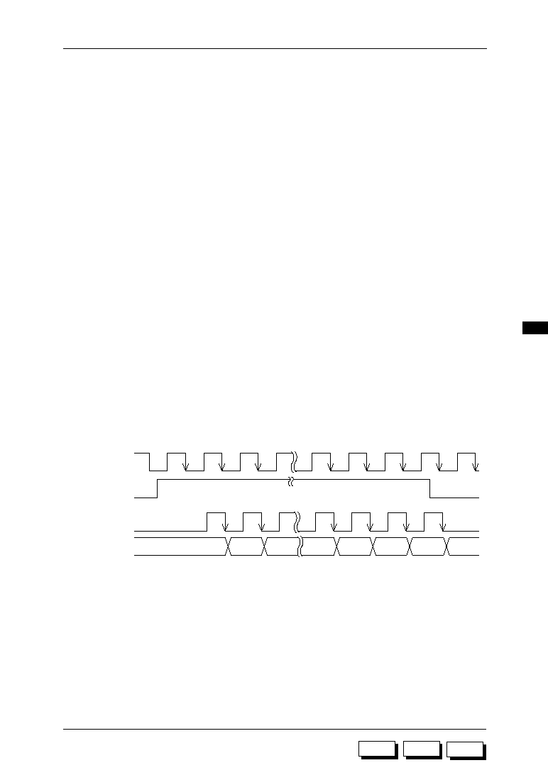
9-17
ML63187/189B/193 User's Manual
Chapter 9 Timers (TIMER)
9
M187
M189B
M193
The operation procedures are as follows.
q
Set PB.1 to the output mode (TM1OVF) secondary function.
w
Write 534FH to the timer data and timer counter registers.
TM1DH = TM1CH = 5H
(bits 15≠12)
TM1DL = TM1CL = 3H
(bits 11≠8)
TM0DH = TM0CH = 4H
(bits 7≠4)
TM0DL = TM0CL = FH
(bits 3≠0)
e
If TM0CON and TM1CON are set to auto-reload mode and TM0RUN is set to
"1", the timer counter register will start to count from 534FH.
r
Before the timer counter register overflows, write the next reload value BFFFH
to the timer data register.
t
When the timer counter register overflows, BFFFH is set to the timer counter
register, timer interrupt TM1INT is generated and timer 1 overflow flag TM1OVF
toggles. The timer counter register continues to count up from BFFFH.
y
Before the timer counter register overflows, write the next reload value 534FH
to the timer data register.
u
When the timer counter register overflows, 534FH is set to the timer counter
register, timer interrupt TM1INT is generated and timer 1 overflow flag TM1OVF
toggles. The timer counter register resumes counting from address 534FH.
i
Repeat steps 4 through 7. This allows a user-defined pulse to be output from
PB.1/TM1OVF.
o
Halt the count by resetting TM0RUN to "0".
Figure 9-7 shows TM0RUN count start/halt timing.
Selected clock
Timer counter
register
TM0RUN
M
M+1
M+2
N≠3
N≠1
N
Timer clock
N≠4
N≠2
Figure 9-7 TM0RUN Count Start/Halt Timing
When TM0RUN is set to "1", the timer counter starts to count from the second falling edge
of the selected clock. When TM0RUN is reset to "0", the counter stops counting at the falling
edge of the selected clock which appears immediately after the TM0RUN falling edge.

9-18
ML63187/189B/193 User's Manual
Chapter 9 Timers (TIMER)
M187
M189B
M193
9.4.6 Capture Mode Operation
Timer 0 and timer 1 can be used as capture mode timers.
In a capture mode, a change in the capture input (PB.0/TM0CAP, PB.1/TM1CAP) level during
operation of the timer counter register triggers loading of the value of the timer counter register
into the timer data register.
Methods to set the capture mode for each timer are listed below.
∑
Timer 0: Set TM0ECAP (bit 1 of TM0CON0) to "1", and set FMEAS0 (bit 2 of
TM0CON0) to "0".
∑
Timer 1: Set TM1ECAP (bit 1 of TM1CON0) to "1".
In the capture mode, reloading the timer data register data into the timer counter register is
inhibited, and when the timer counter register overflows, counting is restarted from 00H.
When a capture occurs, the capture flags (TM0CAP, TM1CAP) of the timer status registers
(TM0STAT, TM1STAT) are set to "1". Additional captures are disabled while the capture flags
are "1". The capture flags are assigned to bit 0 of the timer status registers, and are
automatically cleared to "0" when the timer status registers are read.
If both the TM1CL1 and TM1CL0 bits of the timer 1 control register 1 (TM1CON1) are set to
"1" and timer 0 overflow is selected as the clock, the 16-bit capture mode will be set. In this
case, the PB.0/TM0CAP pin is the capture trigger input.
Figure 9-8 shows the timer 0 capture mode timing for pulse width measurement.
TM0CH, TM0CL
TM0DH, TM0DL
TM0RUN
TM0ECAP
TM0INT
PB.0/TM0CAP input
TM0CAP
XI0INT
50H
F0H
60H
E0H
®u
w
ÿ
y
i
e
∆
r∆
q
®t
®o
00H
50H
F0H
60H
E0H
t3
t2
t1
Figure 9-8 Capture Mode Timing
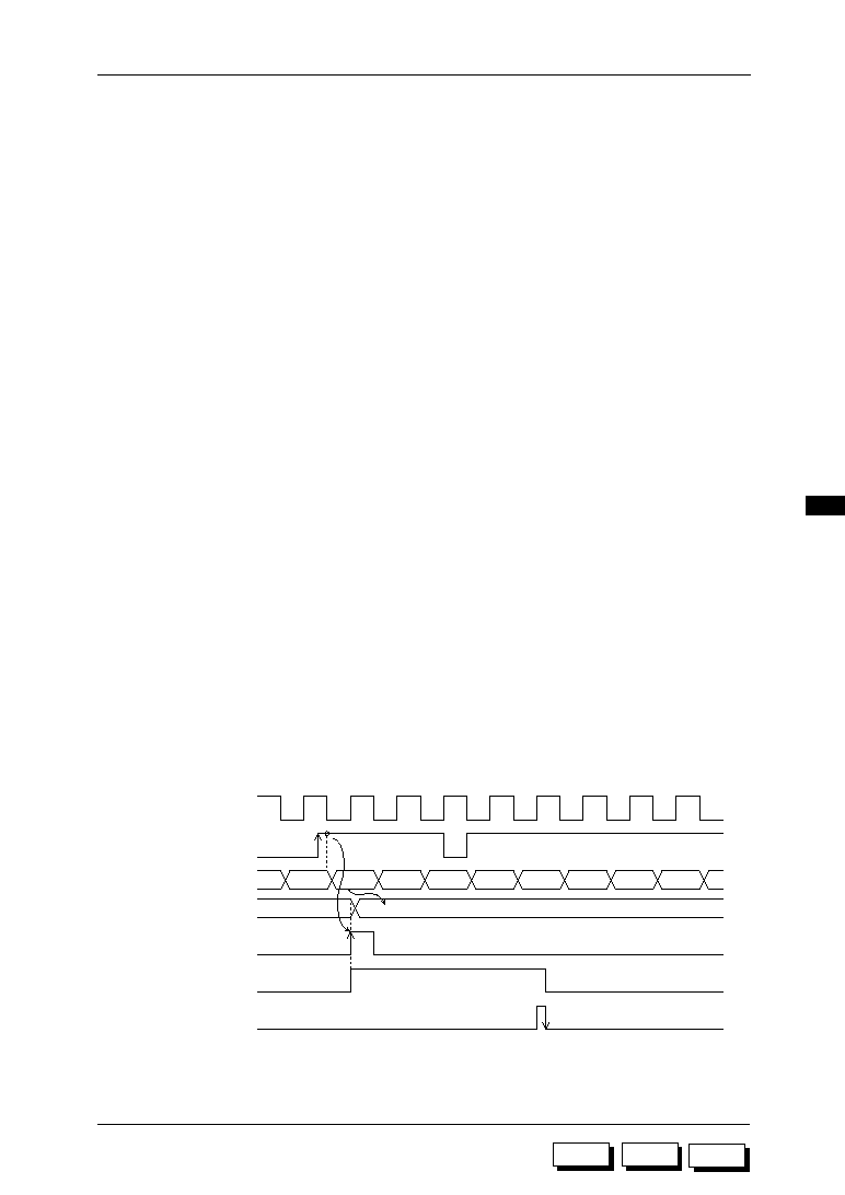
9-19
ML63187/189B/193 User's Manual
Chapter 9 Timers (TIMER)
9
M187
M189B
M193
The operation procedure is listed below.
q
Set PB.0/TM0CAP to input mode, and enable XI0INT and TM0INT.
w
Clear all bits of the timer counter registers and timer data registers to zero.
e
Set TM0CON0 to the capture mode, and set TM0RUN to "1" to begin upward
counting.
r
If the PB.0/TM0CAP input changes, the TM0CH/TM0CL value is captured by
TM0DH/TM0DL and TM0CAP is set to "1" (first capture). The CPU detects this
through XI0INT and reads the values of TM0DH/TM0DL.
t
After the TM0DH/TM0DL read is complete, TM0CAP is cleared to "0" to wait for
the next capture.
y
If the PB.0/TM0CAP input changes, repeat operations
r
and
t
(second
capture).
The high-level pulse width t1 of the PB.0 input can be determined as follows.
t1 = (F0H ≠ 50H)
•
t
CLK
t
CLK
: TMCLK cycle
u
TM0INT is generated when the timer counter register overflows. When overflow
occurs, the timer counter register changes from FFH to 00H and continues upward
counting.
i
If the PB.0/TM0CAP input changes, repeat operations
r
and
t
(third capture).
Because the counter overflows once during the interval between the second
capture and the third capture, the low-level pulse width t2 of the PB.0 input can be
determined as follows.
t2 = (60H ≠ F0H + 100H)
•
t
CLK
o
While TM0CAP = "1", there is no capture even when PB.0/TM0CAP changes.
Figure 9-9 shows the capture timing and Figure 9-10 shows the capture signal (CAPT)
generator circuit.
m+5
m+4
m+3
m+2
m+1
m
m+6
m+7
m+8
m+1
Timer clock
PB.0/TM0CAP input
TM0CH, TM0CL
TM0DH, TM0DL
Capture signal
(CAPT)
TM0CAP
TM0STAT READ
Figure 9-9 Capture Timing

9-20
ML63187/189B/193 User's Manual
Chapter 9 Timers (TIMER)
M187
M189B
M193
CAPT
D
Q
D
Q
D
Q
PB.0/TM0CAP input
Timer clock
TM0ECAP
TM0CAP
Q
Figure 9-10 Capture Signal (CAPT) Generator Circuit
!
Note:
The maximum delay from a PB.0/TM0CAP input level change until capture is one cycle of the
timer clock.
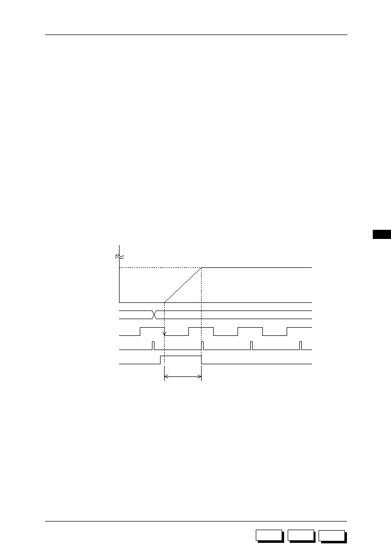
9-21
ML63187/189B/193 User's Manual
Chapter 9 Timers (TIMER)
9
M187
M189B
M193
9.4.7 Frequency Measurement Mode Operation
The frequency measurement mode is used to measure the frequency of the RC oscillator
clock, which has wide product variation.
Timers 0 and 1, and timers 2 and 3 can be used in the frequency measurement mode. These
timers are set as follows for the frequency measurement mode:
∑
Timer 0:
Set FMEAS0 (bit 2 of TM0CON0) to "1", and set TM0ECAP (bit 1 of
TM0CON0) and TM0RUN (bit 0 of TM0CON0) to "0".
∑
Timer 1:
Set TM1ECAP (bit 1 of TM1CON0) and TM1RUN (bit 0 of TM1CON0)
to "0".
∑
Timer 2:
Set FMEAS2 (bit 2 of TM2CON0) to "1", and set TM2RUN (bit 0 of
TM2CON0) to "0".
∑
Timer 3:
Set TM3RUN (bit 0 of TM3CON0) to "0".
The count obtained in the frequency measurement mode can be used to determine the auto-
reload mode timer data register value, thereby making the timer overflow to generate various
signals with required cycles. In the ML63193, the timer 3 interrupt signal (TM3INT) is used
as the baud rate clock.
Figure 9-11 indicates frequency measurement mode timing when timers 2 and 3 are used as
a 16-bit timer.
FFFF
N1
TM3CH
TM3CL
TM2CH
TM2CL
TM3DH, TM3DL
TM2DH, TM2DL
64 Hz
437C
FMEAS2
437/32768 s
(H)
q
ÿ
t
ÿ
e
w
r
0000
Figure 9-11 Frequency Measurement Mode Timing
The operation sequence for Figure 9-11 is as follows.
q
Timer 3 control registers 0 and 1 (TM3CON0, TM3CON1) are set for 16-bit timer
mode, and the timer counter and timer data register are cleared to "0". Enable the
high-speed clock by the frequency control register (FCON) and the timer clock is
set to HSCLK.
w
Wait 10 ms or more in the ceramic oscillation mode or 300
m
s or more in the RC
oscillation mode after starting the high-speed clock and set FMEAS2 to "1" to enter
the frequency measurement mode.
e
When FMEAS2 is "1", the counter starts at the 64 Hz falling edge.
r
When the 437C signal is "1", FMEAS2 is reset to "0", and the counter stops at the
falling edge of the next clock. The 437C signal is a pulse signal which rises in 437/
32768 seconds after the 64 Hz falling edge.
t
Timer counter register value N1 is read.

9-22
ML63187/189B/193 User's Manual
Chapter 9 Timers (TIMER)
M187
M189B
M193
Assuming that the ceramic oscillation clock is exactly 2 MHz, value N1 read from the timer
counter register is:
N1 = 2000000
•
437/32768
= 26672 (decimal)
= 6830 (hexadecimal)
= 0110 1000 0011 0000 (binary)
(truncated)
Because 437/32768 seconds are equivalent to 128 clocks at 9600 Hz (more precisely, 9598
Hz), a division of the count by 128 provides the frequency ratio (N2) between 2 MHz and 9600
Hz. Because 128 = 2
7
, that can be determined by merely truncating the righthand seven digits
of N1 (binary), yielding.
N2 = 26672/128 = 011010000 (binary)
= D0 (hexadecimal)
= 208 (decimal)
This indicates that 9600 Hz is about 208 times the cycle of 2 MHz, which means that the timer
data register should be set to FF30H so that the counter overflows every 208 counts of the
2 MHz clock in auto-reload mode. As a result, overflow produces a TM3INT cycle t
TM3INT
of
t
TM3INT
= 1/2000000
•
208 = 0.104 ms (9615 Hz)
In the same way, assuming that RC oscillation clock is 600 kHz due to manufacturing
variation, we get
N1 = 600000
•
437/32768 = 8001 (decimal)
= 1F41 (hexadecimal)
= 0001 1111 0100 0001 (binary)
(truncated)
Truncating the righthand seven digits of N1 (binary), we get
N2 = 8001/128 = 000111110 (binary)
= 3E (hexadecimal)
= 62 (decimal)
Set the timer data register to FFC2H so that the counter overflows every 62 counts of the 600
kHz clock in auto-reload mode. As a result, overflow produces a TM3INT cycle t
TM3INT
of
t
TM3INT
= 1/600000
•
62 = 0.10333 ms (9677 Hz)
In this way the frequency measurement mode can be applied to generate TM3INT signals
with precision cycles. These TM3INT signals can be supplied to the serial port as a baud rate
clock.
Changing the value of N2 makes it possible to generate baud rates of 4800 Hz, 2400 Hz or
user-defined rates. The precision of the generated baud rate clock is within
±
2% for 9600 Hz,
and within
±
1% for 4800 Hz or lower.
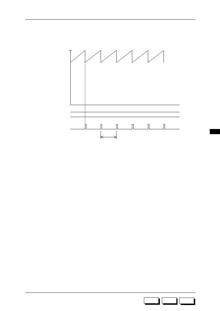
9-23
ML63187/189B/193 User's Manual
Chapter 9 Timers (TIMER)
9
M187
M189B
M193
Figure 9-12 illustrates the operation of timer 3 interrupt for an RC oscillator clock frequency
of 600 kHz.
(H)
FFFF
FFC2
TM3CH
TM3CL
TM2CH
TM2CL
0000
TM3DH, TM3DL
TM2DH, TM2DL
TM3INT
(9677 Hz)
FFC2
0.10333 ms
Figure 9-12 Timer 3 Interrupt (TM3INT) Generation

9-24
ML63187/189B/193 User's Manual
Chapter 9 Timers (TIMER)
M187
M189B
M193

M189B
M187
M193
Chapter 10
10
100 Hz Timer Counter
(100HzTC)
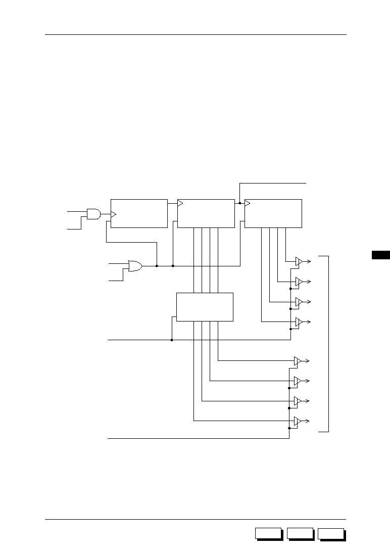
10-1
ML63187/189B/193 User's Manual
Chapter 10 100 Hz Timer Counter (100HzTC)
10
M187
M189B
M193
Figure 10-1 100 Hz Timer Counter Configuration
Chapter 10 100 Hz Timer Counter (100HzTC)
10.1 Overview
The 100 Hz timer counter has a circuit that divides the TBC6 output (512 Hz) of the time base
counter to generate a 10 Hz interrupt. The 100 Hz timer consists of a 5/6-base counter and
two decimal counters.
10.2 100 Hz Timer Counter Configuration
Figure 10-1 indicates the configuration of the 100 Hz timer counter.
5/6-base counter
decimal counter
decimal counter
4-bit latch
T10HzINT
bit 3
bit 2
bit 1
bit 0
bit 3
bit 2
bit 1
bit 0
R
R
L
Data
bus
T100CR READ
T10CR READ
T100CR WRITE
T10CR WRITE
ECNT
512 Hz
T100CR
T10CR
R
10-2
ML63187/189B/193 User's Manual
Chapter 10 100 Hz Timer Counter (100HzTC)
M187
M189B
M193
10.3 100 Hz Timer Counter Registers
(1) 100 Hz timer counter control register (T100CON)
This is a 4-bit special function register (SFR) controlling the 100 Hz timer counter.
--
--
--
ECNT
T100CON (066H)
(R/W)
bit 3
bit 2
bit 1
bit 0
Count start/stop select
0 : Count stop (initial value)
1 : Count start
100C3
100C2
100C1
100C0
T100CR (064H)
(R/W)
bit 3
bit 2
bit 1
bit 0
(2) 100 Hz counter register (T100CR)
This is a 4-bit special function register (SFR) to read the 100 Hz counter of the 100 Hz timer
counter. The content of the T100CR is latched by a 4-bit latch in T10CR read operation, so
the value of the T100CR must always be read after reading T10CR.
When data is written in T100CR, both T100CR and T10CR are reset to "0".
bit 0: ECNT
This bit controls count start/stop for the 100 Hz timer counter internal counter.
Count starts when set to "1". At system reset the value is reset to "0" and counting
is stopped.
10C3
10C2
10C1
10C0
T10CR (065H)
(R/W)
bit 3
bit 2
bit 1
bit 0
(3) 10 Hz counter register (T10CR)
A 4-bit special function register (SFR) to read the 10 Hz counter in the 100 Hz timer counter.
When data is written in T10CR, both T100CR and T10CR are reset to "0".

10-3
ML63187/189B/193 User's Manual
Chapter 10 100 Hz Timer Counter (100HzTC)
10
M187
M189B
M193
10.4 100 Hz Timer Counter Operation
The 100 Hz timer counter begins counting when bit 0 (ECNT) of the 100 Hz timer counter
control register (T100CON) is set to "1". The 512 Hz output of the time base counter is divided
into 100 Hz by the 5/6-base counter.
The 100 Hz signal is input to the 100 Hz counter (T100CR) and the carry output of that counter
is input to the 10 Hz counter (T10CR). The 10HzINT signal, which is the carry output (10 Hz)
of the T100CR 100 Hz counter also generates an interrupt request, setting bit 3 (Q10Hz) of
interrupt request registers 3 (IRQ3) to "1".
If either T100CR or T10CR is written to, both are reset to "0". The write data used has no
significance. For example, the "MOV T100CR, A" instruction is not dependent on the
contents of the accumulator.
If T10CR is read, the contents of T100CR at that time are latched to the 4-bit latch. Therefore,
the contents of T100CR at the time T10CR is read can be read correctly.

10-4
ML63187/189B/193 User's Manual
Chapter 10 100 Hz Timer Counter (100HzTC)
M187
M189B
M193

M189B
M187
M193
Chapter 11
11
Watchdog Timer (WDT)

11-1
ML63187/189B/193 User's Manual
Chapter 11 Watchdog Timer (WDT)
11
M187
M189B
M193
Chapter 11 Watchdog Timer (WDT)
11.1 Overview
The watchdog timer is a circuit to detect CPU malfunction. The WDT consists of a 9-bit
watchdog timer counter (WTDC) counting the 256 Hz output of the TBC7 of the time base
counter (TBC), and a watchdog timer control register (WDTCON) to start and clear WDTC.
11.2 Watchdog Timer Configuration
Figure 11-1 shows the configuration of the watchdog timer.
"5H" detection
and latch
"0AH" detection
1/2
9
WDTC
QWDACK
(internal reception signal)
RESETS
(system reset)
WDTINT
(interrupt request)
256 Hz
(from time base counter)
Watchdog timer counter
R
Data bus
4
Internal pointer
WDTCON
WDTCON
WRITE
T
Q
R
4
Figure 11-1 Watchdog Timer Configuration
11-2
ML63187/189B/193 User's Manual
Chapter 11 Watchdog Timer (WDT)
M187
M189B
M193
11.3 Watchdog Timer Control Register (WDTCON)
The watchdog timer control register (WDTCON) is a 4-bit write only special function register
(SFR) used to start/clear the watchdog timer counter (WDTC).
11.4 Watchdog Timer Operation
At system reset, WDTC (watchdog timer counter) stops counting.
WDTC begins counting by writing "5H" to WDTCON (watchdog timer control register) while
the internal pointer is "0", and then writing "0AH" (while the internal pointer is "1").
The internal pointer is cleared to "0" at system reset or when WDTC overflows, and toggles
every time a write operation to WDTCON is performed.
After WDTC is activated, WDTC is cleared by writing "5H" to WDTCON while the internal
pointer is "0", and then writing "0AH" while the internal pointer is "1". When WDTC overflows
(1FFH
000H), a watchdog timer interrupt request (WDTINT) is generated. WDTINT cannot
be disabled by the software (non-maskable interrupt) and has the highest level of interrupt
priority.
The WDTC overflow cycle (T) is given by:
128
•
512
T = = 2 s
32768 (Hz)
The minus deviation (t) of the WDTC overflow cycle is given by:
128
t = = approximately 3.9 ms
32768 (Hz)
Therefore, the WDTC clear cycle (Ct) can be computed as follows.
Ct = T ≠ t = 2 s ≠ 3.9 ms = 1.9961 s
If 32.768 kHz is to be used as the low-speed clock, the software must be programmed to clear
WDTC within 1.9961 s.
If the CPU malfunctions due to a power failure or other factor and the WDTC cannot be cleared
normally, WDTC will overflow and WDTINT will be generated. Program the watchdog timer
interrupt routine to handle recovery operations by returning to the normal routine.
!
Note:
The watchdog timer cannot detect all operating faults. If the CPU malfunctions but WDTC can
still be cleared, a fault will not be detected.
d3
d2
d1
d0
WDTCON (09FH)
(W)
bit 3
bit 2
bit 1
bit 0
11-3
ML63187/189B/193 User's Manual
Chapter 11 Watchdog Timer (WDT)
11
M187
M189B
M193
Figure 11-2 shows a flowchart of watchdog timer processing.
System reset
Write "5H"
to WDTCON
Write "0AH"
to WDTCON
Write "5H"
to WDTCON
Processing
Write "0AH"
to WDTCON
Processing
WDT operation is stopped
Internal pointer "0"
WDT operation is started
Internal pointer "1"
∆ "0"
Internal pointer "0"
∆"1"
Processing
time should not
exceed 1.9961 s
Internal pointer "0"
∆"1"
WDTC is cleared
Internal pointer "1"
∆"0"
Figure 11-2 Watchdog Timer Processing Flowchart
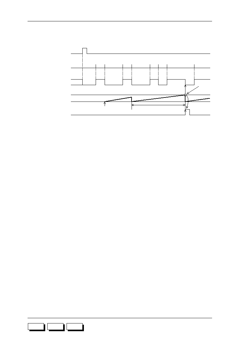
11-4
ML63187/189B/193 User's Manual
Chapter 11 Watchdog Timer (WDT)
M187
M189B
M193
Figure 11-3 shows the timing chart for watchdog timer operation.
1.9 to 2.0 s
(Interrupt request)
Data:
Fault occurrence
ÿ
Overflow
System reset
WDTCON
write signal
Internal pointer
Watchdog timer counter
(WDTC) content
WDTINT
(interrupt request signal)
w
5
e
A
r
5
t
A
u
5
5
q
y
5
i
A
o
Start
The watchdog timer operating sequence is listed below.
q
System reset clears the internal pointer and WDTC.
w
Write "5H" to WDTCON. (Internal pointer 0
∆
1)
e
Write "0AH" to WDTCON to start WDTC. (Internal pointer 1
∆
0)
r
Write "5H" to WDTCON. (Internal pointer 0
∆
1)
t
Write "0AH" to WDTCON to clear WDTC. (Internal pointer 1
∆
0)
y
Write "5H" to WDTCON. (Internal pointer 0
∆
1)
u
After a fault occurs, "5H" is written to WDTCON but is not accepted since the
internal pointer is "1". (Internal pointer 1
∆
0)
i
"0AH" is written to WDTCON, but since the internal pointer is "0" and the write of
"5H" in step
u
was not accepted, WDTC will not be cleared. (Internal pointer 0
∆
1)
o
Because WDTC was not cleared, overflow of WDTC will generate the watchdog
timer interrupt WDTINT. At this time, the internal pointer is cleared to "0".
Figure 11-3 Watchdog Timer Operation Timing Chart

M187
M189B
M193
Chapter 12
12
Ports (INPUT, I/O PORT)

12-1
ML63187/189B/193 User's Manual
Chapter 12 Ports (INPUT, I/O PORT)
12
M187
M189B
M193
Chapter 12 Ports (INPUT, I/O PORT)
12.1 Overview
The ML63187 has two 4-bit I/O ports.
The ML63189B has one 4-bit input port and four 4-bit I/O ports.
The ML63193 has one 4-bit input port and five 4-bit I/O ports.
The V
DDI
(interface power supply) pin supplies power to the ports.
If a port is to be connected to an external device that operates on a different power supply,
the power supply of the external device must be fed to the V
DDI
pin.
!
Note:
Since V
DDI
is separated from the positive power supply pin (V
DD
), power must be supplied
to the V
DDI
pin.
12.2 Ports List
The ports of the ML63187, ML63189B, and ML63193 are shown in Table 12-1.
Table 12-1 Ports List
Port
Interrupt
Sedondary
function
ML63187
ML63189B
Port 0
q
q
--
q
--
--
Port 9
q
q
--
q
Port A
--
q
q
q
q
Port B
q
Port E
q
q
q
q
I/O
I
I/O
Page
12-2
12-7
12-7
12-12
12-25
ML63193
q
q
q
q
q
--
--
Port C
q
q
12-18
q
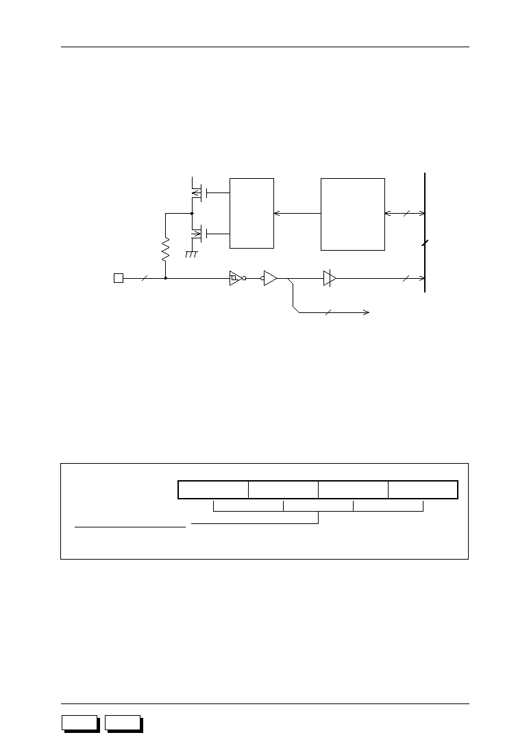
12-2
ML63187/189B/193 User's Manual
Chapter 12 Ports (INPUT, I/O PORT)
M187
M189B
M193
12.3 Port 0 (P0.0≠P0.3)
12.3.1 Port 0 Configuration
The ML63189B and ML63193 have Port 0, a 4-bit input-only port.
Figure 12-1 shows the configuration of port 0.
Pull-up/
pull-down
control
P0CON0
P0CON1
4
4
V
DDI
4
P0.0≠P0.3
V
SS
Read P0D
4
4
P0.0≠P0.3
(to external interrupt 5
control circuit)
Data bus
Figure 12-1 Input-Only Port (Port 0) Configuration
12.3.2 Port 0 Registers
(1) Port 0 data register (P0D)
The port 0 data register (P0D) is a 4-bit read-only special function register (SFR) used to read
the pin level of each bit of port 0.
P03
P02
P01
P00
P0D (000H)
(R)
bit 3
bit 2
bit 1
bit 0
Pin level of each bit of port 0
0: "L" level
1: "H" level
M189B
M193
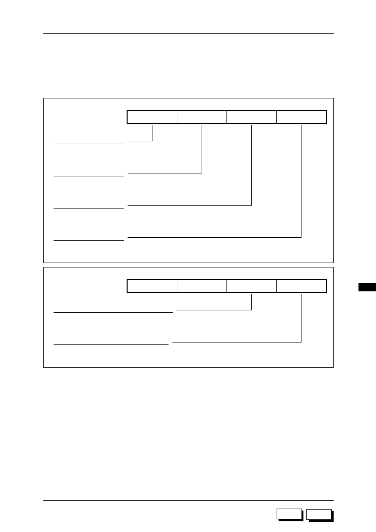
12-3
ML63187/189B/193 User's Manual
Chapter 12 Ports (INPUT, I/O PORT)
12
M187
M189B
M193
(2) Port 0 control registers (P0CON0, P0CON1)
The port 0 control registers 0/1 (P0CON0, P0CON1) are 4-bit special function registers
(SFRs) that select pull-up or pull-down resistors and select the external interrupt sampling
frequency of Port 0 secondary function.
P03MD
P02MD
P01MD
P00MD
P0CON0 (010H)
(R/W)
bit 3
bit 2
bit 1
bit 0
Port 0.3 input mode select
0: Input with pull-up/pull-down resistor (initial value)
1: High impedance input
Port 0.2 input mode select
0: Input with pull-up/pull-down resistor (initial value)
1: High impedance input
Port 0.1 input mode select
0: Input with pull-up/pull-down resistor (initial value)
1: High impedance input
Port 0.0 input mode select
0: Input with pull-up/pull-down resistor (initial value)
1: High impedance input
--
--
P0PUD
P0F
P0CON1 (011H)
(R/W)
bit 3
bit 2
bit 1
bit 0
Port 0 pull-up/pull-down resistor mode select
0: Inputs with pull-down resistors (initial value)
1: Inputs with pull-up resistors
External interrupt sampling frequency select
0: 128 Hz sampling (initial value)
1: 4 kHz sampling
bit 1: P0PUD
This bit is used to select pull-up or pull-down resistors when any of the port 0 pins
are selected by P0CON0 as an input with pull-up/pull-down resistor.
Setting P0PUD to "0" selects pull-down resistors, and setting to "1" selects pull-
up resistors.
Individual specification of pull-down or pull-up resistors for the pins of port 0.0
to 0.3 is not possible.
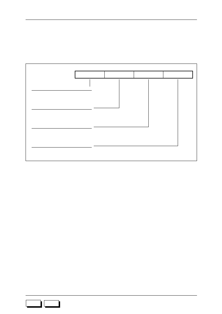
12-4
ML63187/189B/193 User's Manual
Chapter 12 Ports (INPUT, I/O PORT)
M187
M189B
M193
(3) Port 0 interrupt enable register (P0IE)
The port 0 interrupt enable register (P0IE) is a 4-bit special function register (SFR) that
enables/disables individual bits when port 0 is used as an external interrupt.
At system reset, all bits in the port interrupt enable register are cleared to "0" and port 0 is
initialized to the interrupt disabled state.
P03IE
P02IE
P01IE
P00IE
P0IE (012H)
(R/W)
bit 3
bit 2
bit 1
bit 0
Port 0.3 interrupt disable/enable select
0: Interrupt disabled (initial value)
1: Interrupt enabled
Port 0.2 interrupt disable/enable select
0: Interrupt disabled (initial value)
1: Interrupt enabled
Port 0.1 interrupt disable/enable select
0: Interrupt disabled (initial value)
1: Interrupt enabled
Port 0.0 interrupt disable/enable select
0: Interrupt disabled (initial value)
1: Interrupt enabled
M189B
M193

12-5
ML63187/189B/193 User's Manual
Chapter 12 Ports (INPUT, I/O PORT)
12
M187
M189B
M193
12.3.3 Port 0 External Interrupt Function (External Interrupt 5)
An external interrupt (external interrupt 5) is assigned to port 0 as a secondary function.
Individual bits can be enabled/disabled for external interrupt 5.
External interrupt generation for each input of port 0 is triggered by the falling edge of either
the 128 Hz or 4 kHz sampling clock from the time base counter.
After the port level changes, interrupt request signal XI5INT is output and external interrupt
5 request flag (QXI5) is set. The maximum time delay from the change in port level until setting
QXI5 is one cycle of the sampling clock (128 Hz or 4 kHZ).
Because the port 0 external interrupt 5 is set by a level change at any of the port 0 inputs, each
bit of the port must be read to determine which bit of port 0 generated the interrupt.
External interrupt 5 is generated during the following states.
P0PUD = "0" (initial value: inputs with pull-down resistors) setting
With all P0.0 to P0.3 inputs at a "L" level, external interrupt 5 is generated when
any port 0 input changes to a "H" level.
With any of P0.0 to P0.3 inputs at a "H" level, external interrupt 5 is generated when
all the port 0 inputs change to a "L" level.
P0PUD = "1" (initial value: inputs with pull-up resistors) setting
With all P0.0 to P0.3 inputs at a "H" level, external interrupt 5 is generated when
any port 0 input changes to a "L" level.
With any of P0.0 to P0.3 inputs at a "L" level, external interrupt 5 is generated when
all the port 0 inputs change to a "H" level.
The interrupt vector address for external interrupt 5 is 001EH.
Figure 12-2 shows the timing for generation of external interrupt 5.
Figure 12-3 shows an equivalent circuit of external interrupt 5 control.
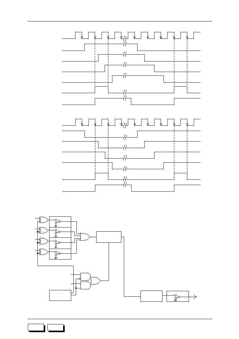
12-6
ML63187/189B/193 User's Manual
Chapter 12 Ports (INPUT, I/O PORT)
M187
M189B
M193
128 Hz or
4 kHz
P0.0
P0.1
P0.2
P0.3
XI5INT
QXI5
(a) When P0PUD = 0
(b) When P0PUD = 1
128 Hz or
4 kHz
P0.0
P0.1
P0.2
P0.3
XI5INT
QXI5
Figure 12-2 Interrupt Generation Timing of External Interrupt 5
Figure 12-3 Equivalent Circuit of External Interrupt 5 Control
Level change
detection circuit
IE1.3
EXI5
To interrupt
priority encoder
circuit
128 Hz
4 kHz
P0CON1
P0F
Sampling signal
IRQ1
IE1
IRQ1.3
QXI5
XI5INT
P00IE
P01IE
P02IE
P03IE
P0IE
P0.0
P0.1
P0.2
P0.3
P0PUD
M189B
M193

12-7
ML63187/189B/193 User's Manual
Chapter 12 Ports (INPUT, I/O PORT)
12
M187
M189B
M193
12.4 Port 9, Port A (P9.0≠P9.3, PA.0≠PA.3)
The ML63189B and ML63193 have Port 9 and Port A, 4-bit input/output ports.
12.4.1 Port 9, Port A Configuration
The circuit configurations for ports 9 and A are shown in Figure 12-4.
Data bus
Output
port
control
P9D
P9DIR
P9CON0
P9CON1
Pull-up/
pull-down
control
4
V
DDI
V
DDI
P9.0≠P9.3
V
SS
V
SS
Output
port
control
PAD
PADIR
PACON0
PACON1
Pull-up/
pull-down
control
4
V
DDI
V
DDI
PA.0≠PA.3
V
SS
V
SS
4
4
Figure 12-4 Input/Output Port (Ports 9 and A) Configuration
12-8
ML63187/189B/193 User's Manual
Chapter 12 Ports (INPUT, I/O PORT)
M187
M189B
M193
P93DIR
P92DIR
P91DIR
P90DIR
P9DIR (029H)
(R/W)
bit 3
bit 2
bit 1
bit 0
Port 9 input/output setting
0: Input (initial value)
1: Output
∑ Port A
12.4.2 Port 9, Port A Registers
(1) Port 9, Port A direction registers (P9DIR, PADIR)
The port 9 direction register (P9DIR) and port A direction register (PADIR) are 4-bit special
function registers (SFRs) which specify the port input/output direction for each bit. Pins
corresponding to P9DIR and PADIR bits set to "0" are input, and those corresponding to bits
set to "1" are output.
At system reset all bits in P9DIR and PADIR are set to "0", and ports 9 and A are initialized
to input mode.
∑ Port 9
PA3DIR
PA2DIR
PA1DIR
PA0DIR
PADIR (02CH)
(R/W)
bit 3
bit 2
bit 1
bit 0
Port A input/output setting
0: Input (initial value)
1: Output
M189B
M193
12-9
ML63187/189B/193 User's Manual
Chapter 12 Ports (INPUT, I/O PORT)
12
M187
M189B
M193
P93
P92
P91
P90
P9D (009H)
(R/W)
bit 3
bit 2
bit 1
bit 0
Port 9 input/output data
∑ Port A
PA3
PA2
PA1
PA0
PAD (00AH)
(R/W)
bit 3
bit 2
bit 1
bit 0
Port A input/output data
At system reset all bits in the port 9 and A data registers are set to "0". When data is written
to a port data register, the actual pin change timing is at the rising edge of the system clock
for state 2 of the write instruction.
Figure 12-5 shows port change timing.
S1
S2
Old data
New data
CLK
Ports 9, A
Write instruction
Figure 12-5 Port Change Timing
(2) Port 9, Port A data registers (P9D, PAD)
The port 9 data register (P9D) and port A data register (PAD) are 4-bit special function
registers (SFRs) used to set the output values for the ports.
When a bit in the port direction register (P9DIR, PADIR) is set to "1" to select the output mode,
the content of the corresponding bit in the port data register (P9D, PAD) is output to the port
(port 9, port A).
When a bit in the port data register (P9D, PAD) is read with the corresponding port direction
register bit set to output, the value of the bit in the port data register is read.
When a bit in the port data register (P9D, PAD) is read with the corresponding port direction
register bit set to "0" (input mode), the level of the corresponding pin is read.
∑ Port 9
12-10
ML63187/189B/193 User's Manual
Chapter 12 Ports (INPUT, I/O PORT)
M187
M189B
M193
(3) Port 9, Port A control registers (P9CON0, P9CON1, PACON0, PACON1)
The port 9 control registers 0/1 (P9CON0, P9CON1) and port A control registers 0/1
(PACON0, PACON1) are 4-bit special function registers (SFRs) used to select port input/
output mode.
The input mode may be pull-down resistor input, pull-up resistor input or high-impedance
input.
The output mode may be CMOS output, N-channel open drain output, P-channel open drain
output or high-impedance output.
∑ Port 9
P91MD1
P91MD0
P90MD1
P90MD0
P9CON0 (027H)
(R/W)
bit 3
bit 2
bit 1
bit 0
Port 9.1 input/output mode select
Input mode
bit 3
0
1
•
bit 2
0
0
1
: Input with pull-down resistor (initial value)
: Input with pull-up resistor
: High-impedance input
Port 9.0 input/output mode select
Input mode
bit 1
0
1
•
bit 0
0
0
1
: Input with pull-down resistor (initial value)
: Input with pull-up resistor
: High-impedance input
Output mode
bit 3
0
0
1
1
bit 2
0
1
0
1
: CMOS output (initial value)
: N-channel open drain output
: P-channel open drain output
: High-impedance output
Output mode
bit 1
0
0
1
1
bit 0
0
1
0
1
: CMOS output (initial value)
: N-channel open drain output
: P-channel open drain output
: High-impedance output
P93MD1
P93MD0
P92MD1
P92MD0
P9CON1 (028H)
(R/W)
bit 3
bit 2
bit 1
bit 0
Port 9.3 input/output mode select
Input mode
bit 3
0
1
•
bit 2
0
0
1
: Input with pull-down resistor (initial value)
: Input with pull-up resistor
: High-impedance input
Port 9.2 input/output mode select
Input mode
bit 1
0
1
•
bit 0
0
0
1
: Input with pull-down resistor (initial value)
: Input with pull-up resistor
: High-impedance input
Output mode
bit 3
0
0
1
1
bit 2
0
1
0
1
: CMOS output (initial value)
: N-channel open drain output
: P-channel open drain output
: High-impedance output
Output mode
bit 1
0
0
1
1
bit 0
0
1
0
1
: CMOS output (initial value)
: N-channel open drain output
: P-channel open drain output
: High-impedance output
M189B
M193
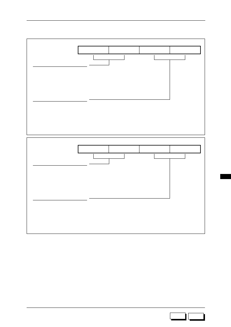
12-11
ML63187/189B/193 User's Manual
Chapter 12 Ports (INPUT, I/O PORT)
12
M187
M189B
M193
∑ Port A
PA1MD1
PA1MD0
PA0MD1
PA0MD0
PACON0 (02AH)
(R/W)
bit 3
bit 2
bit 1
bit 0
Port A.1 input/output mode select
Input mode
bit 3
0
1
•
bit 2
0
0
1
: Input with pull-down resistor (initial value)
: Input with pull-up resistor
: High-impedance input
Port A.0 input/output mode select
Input mode
bit 1
0
1
•
bit 0
0
0
1
: Input with pull-down resistor (initial value)
: Input with pull-up resistor
: High-impedance input
Output mode
bit 3
0
0
1
1
bit 2
0
1
0
1
: CMOS output (initial value)
: N-channel open drain output
: P-channel open drain output
: High-impedance output
Output mode
bit 1
0
0
1
1
bit 0
0
1
0
1
: CMOS output (initial value)
: N-channel open drain output
: P-channel open drain output
: High-impedance output
PA3MD1
PA3MD0
PA2MD1
PA2MD0
PACON1 (02BH)
(R/W)
bit 3
bit 2
bit 1
bit 0
Port A.3 input/output mode select
Input mode
bit 3
0
1
•
bit 2
0
0
1
: Input with pull-down resistor (initial value)
: Input with pull-up resistor
: High-impedance input
Port A.2 input/output mode select
Input mode
bit 1
0
1
•
bit 0
0
0
1
: Input with pull-down resistor (initial value)
: Input with pull-up resistor
: High-impedance input
Output mode
bit 3
0
0
1
1
bit 2
0
1
0
1
: CMOS output (initial value)
: N-channel open drain output
: P-channel open drain output
: High-impedance output
Output mode
bit 1
0
0
1
1
bit 0
0
1
0
1
: CMOS output (initial value)
: N-channel open drain output
: P-channel open drain output
: High-impedance output

12-12
ML63187/189B/193 User's Manual
Chapter 12 Ports (INPUT, I/O PORT)
M187
M189B
M193
12.5 Port B (PB.0≠PB.3)
The ML63187, ML63189B, and ML63193 have Port B, a 4-bit input/output port.
12.5.1 Port B Configuration
The circuit configuration for port B is shown in Figure 12-6.
Output
port
control
PBD
PBDIR
PBCON0
PBCON1
PBMOD
Pull-up/
pull-down
control
4
2
V
DDI
V
DDI
4
PB.0≠PB.3
V
SS
V
SS
PB.0≠PB.3
(to external interrupt 0
control circuit)
TM0OVF
TM1OVF
(from timer
0, 1 circuits)
TM0CAP, TM1CAP,
T02CK, T13CK
(to timer 0≠3 circuits)
4
4
Data bus
Figure 12-6 Input /Output Port (Port B) Configuration
12-13
ML63187/189B/193 User's Manual
Chapter 12 Ports (INPUT, I/O PORT)
12
M187
M189B
M193
12.5.2 Port B Registers
(1) Port B direction register (PBDIR)
PBDIR is a 4-bit special function register (SFR) which specifies the port input/output direction
for each bit. Pins corresponding to PBDIR bits set to "0" are input, and those corresponding
to bits set to "1" are output.
At system reset all bits in the port B direction register are reset to "0", and port B is initialized
to input mode.
PB3DIR
PB2DIR
PB1DIR
PB0DIR
PBDIR (030H)
(R/W)
bit 3
bit 2
bit 1
bit 0
Port B input/output setting
0: Input (initial value)
1: Output
(2) Port B data register (PBD)
PBD is a 4-bit special function register used to set the output values for port B.
When a bit in the port B direction register (PBDIR) is set to "1" to select the output mode, the
content of the corresponding bit in the port B data register is output to the port B.
When a bit in the port B data register is read with the corresponding PBDIR bit set to output,
the value of the bit in the port B data register is read.
When a bit in the port B data register is read with the corresponding PBDIR bit set to "0" (input
mode), the level of the corresponding pin of port B is read.
PB3
PB2
PB1
PB0
PBD (00BH)
(R/W)
bit 3
bit 2
bit 1
bit 0
Port B output data
At system reset all bits in the port B data register (PBD) are set to "0". When data is written
to the port B data register, the actual pin change timing is at the rising edge of the system clock
for state 2 of the write instruction.
Figure 12-7 indicates port change timing.
S1
S2
Old data
New data
CLK
Port B
Write instruction
Figure 12-7 Port B Change Timing
12-14
ML63187/189B/193 User's Manual
Chapter 12 Ports (INPUT, I/O PORT)
M187
M189B
M193
(3) Port B control registers (PBCON0, PBCON1)
The port B control registers 0/1 (PBCON0, PBCON1) are 4-bit special function registers
(SFRs) used to select port input/output mode.
The input mode can be pull-down resistor input, pull-up resistor input or high-impedance
input.
The output mode can be CMOS output, N-channel open drain output, P-channel open drain
output or high-impedance output.
At system reset all bits in PBCON0 and PBCON1 are set to "0", and port B is initialized to
pull-down resistor input mode and CMOS output mode.
PB1MD1
PB1MD0
PB0MD1
PB0MD0
PBCON0 (02EH)
(R/W)
bit 3
bit 2
bit 1
bit 0
Port B.1 input/output mode select
Input mode
bit 3
0
1
•
bit 2
0
0
1
: Input with pull-down resistor (initial value)
: Input with pull-up resistor
: High-impedance input
Port B.0 input/output mode select
Input mode
bit 1
0
1
•
bit 0
0
0
1
: Input with pull-down resistor (initial value)
: Input with pull-up resistor
: High-impedance input
Output mode
bit 3
0
0
1
1
bit 2
0
1
0
1
: CMOS output (initial value)
: N-channel open drain output
: P-channel open drain output
: High-impedance output
Output mode
bit 1
0
0
1
1
bit 0
0
1
0
1
: CMOS output (initial value)
: N-channel open drain output
: P-channel open drain output
: High-impedance output
PB3MD1
PB3MD0
PB2MD1
PB2MD0
PBCON1 (02FH)
(R/W)
bit 3
bit 2
bit 1
bit 0
Port B.3 input/output mode select
Input mode
bit 3
0
1
•
bit 2
0
0
1
: Input with pull-down resistor (initial value)
: Input with pull-up resistor
: High-impedance input
Port B.2 input/output mode select
Input mode
bit 1
0
1
•
bit 0
0
0
1
: Input with pull-down resistor (initial value)
: Input with pull-up resistor
: High-impedance input
Output mode
bit 3
0
0
1
1
bit 2
0
1
0
1
: CMOS output (initial value)
: N-channel open drain output
: P-channel open drain output
: High-impedance output
Output mode
bit 1
0
0
1
1
bit 0
0
1
0
1
: CMOS output (initial value)
: N-channel open drain output
: P-channel open drain output
: High-impedance output

12-15
ML63187/189B/193 User's Manual
Chapter 12 Ports (INPUT, I/O PORT)
12
M187
M189B
M193
(4) Port B mode register (PBMOD)
PBMOD is a 4-bit special function register (SFR) used to select the sampling frequency when
port B is used as an external interrupt. It is also used to select port B secondary functions other
than external interrupt.
The external interrupt sampling frequency can be selected as either 128 Hz or 4 kHz.
Port B secondary functions are indicated in Table 12-2.
Table 12-2 Port B Secondary Functions
Port
Secondary function
Description
PB.0
TM0CAP
Timer 0 capture input
PB.1
TM1CAP
Timer 1 capture input
PB.2
T02CK
Timer 0, timer 2 external clock input
PB.3
T13CK
Timer 1, timer 3 external clock input
PB.0
TM0OVF
Timer 0 overflow flag output
PB.1
TM1OVF
Timer 1 overflow flag output
PB.0
PB.1
PB.2
INT0
External interrupt 0
PB.3
PBF
--
PB1MOD
PB0MOD
PBMOD (032H)
(R/W)
bit 3
bit 2
bit 1
bit 0
External interrupt sampling frequency select
0: 128 Hz sampling (initial value)
1: 4 kHz sampling
Port B.1 pin function select
0: Input/output function (initial value)
1: Timer 1 overflow flag output (TM1OVF) function
(Goes into output mode irrespective of PB1DIR)
Port B.0 pin function select
0: Input/output port function (initial value)
1: Timer 0 overflow flag output (TM0OVF) function
(Goes into output mode irrespective of PB0DIR)
At system reset all the valid bits in PBMOD are initialized to "0".
12-16
ML63187/189B/193 User's Manual
Chapter 12 Ports (INPUT, I/O PORT)
M187
M189B
M193
(5) Port B interrupt enable register (PBIE)
PBIE is a 4-bit special function register (SFR) that enables/disables individual bits when port
B is used as an external interrupt input.
At system reset, all bits in PBIE are cleared to "0" and port B is initialized to the interrupt
disabled state.
PB3IE
PB2IE
PB1IE
PB0IE
PBIE (031H)
(R/W)
bit 3
bit 2
bit 1
bit 0
Port B.3 interrupt enable/disable select
0: Interrupt disabled (initial value)
1: Interrupt enabled
Port B.2 interrupt enable/disable select
0: Interrupt disabled (initial value)
1: Interrupt enabled
Port B.1 interrupt enable/disable select
0: Interrupt disabled (initial value)
1: Interrupt enabled
Port B.0 interrupt enable/disable select
0: Interrupt disabled (initial value)
1: Interrupt enabled

12-17
ML63187/189B/193 User's Manual
Chapter 12 Ports (INPUT, I/O PORT)
12
M187
M189B
M193
12.5.3 Port B External Interrupt Function (External Interrupt 0)
Port B has external interrupt 0 allocated as secondary function. Individual bits of port B can
be enabled/disabled.
External interrupt generation for port B is triggered by the falling edge of the 128 Hz or 4 kHz
time base counter, which is the sampling clock.
After the port level changes, the interrupt request signal (XI0INT) is output, and the interrupt
request flag (QXI0) is set. The maximum delay for this sequence is one cycle of the sampling
clock (128 Hz or 4 kHz).
Because the port B external interrupt is set by a level change at any of the port B inputs, each
bit of the port must be read to determine which bit of port B generated the interrupt.
The interrupt start address for external interrupt 0 is 0014H.
Figure 12-8 shows the external interrupt 0 generation timing.
Figure 12-9 shows the equivalent circuit for external interrupt 0 control.
Level change
detect circuit
128 Hz
4 kHz
PBMOD
PBF
PB0IE
PB1IE
PB2IE
PB3IE
PBIE
PB.0
PB.1
PB.2
PB.3
IE0.2
EXI0
to interrupt priority
encoder
IRQ0
IE0
IRQ0.2
QXI0
XI0INT
QXI0
(n = 0≠3)
XI0INT
PB.n
128 Hz or
4 kHz
Figure 12-8 External Interrupt 0 Generation Timing
Figure 12-9 External Interrupt 0 Control Equivalent Circuit
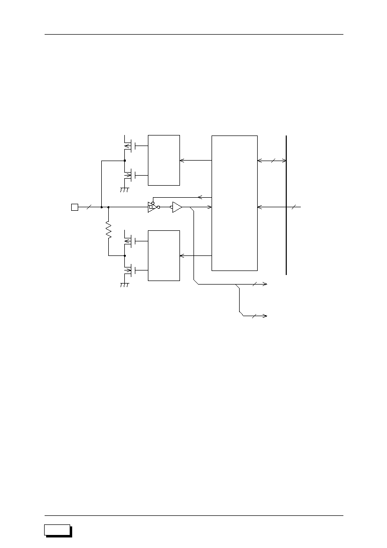
12-18
ML63187/189B/193 User's Manual
Chapter 12 Ports (INPUT, I/O PORT)
M187
M189B
M193
12.6 Port C (PC.0≠PC.3)
The ML63193 has Port C, a 4-bit input/output port.
12.6.1 Port C Configuration
The circuit configuration for port C is shown in Figure 12-10.
Output
port
control
PCD
PCDIR
PCCON0
PCCON1
PCMOD
Pull-up/
pull-down
control
4
3
V
DDI
V
DDI
4
PC.0≠PC.3
V
SS
V
SS
PC.0≠PC.3
(to external interrupt 1
control circuit)
TXC, RXC, TXD
(from serial port)
RXD, TXC, RXC
(to serial port circuits)
4
3
Data bus
Figure 12-10 Input /Output Port (Port C) Configuration
M193
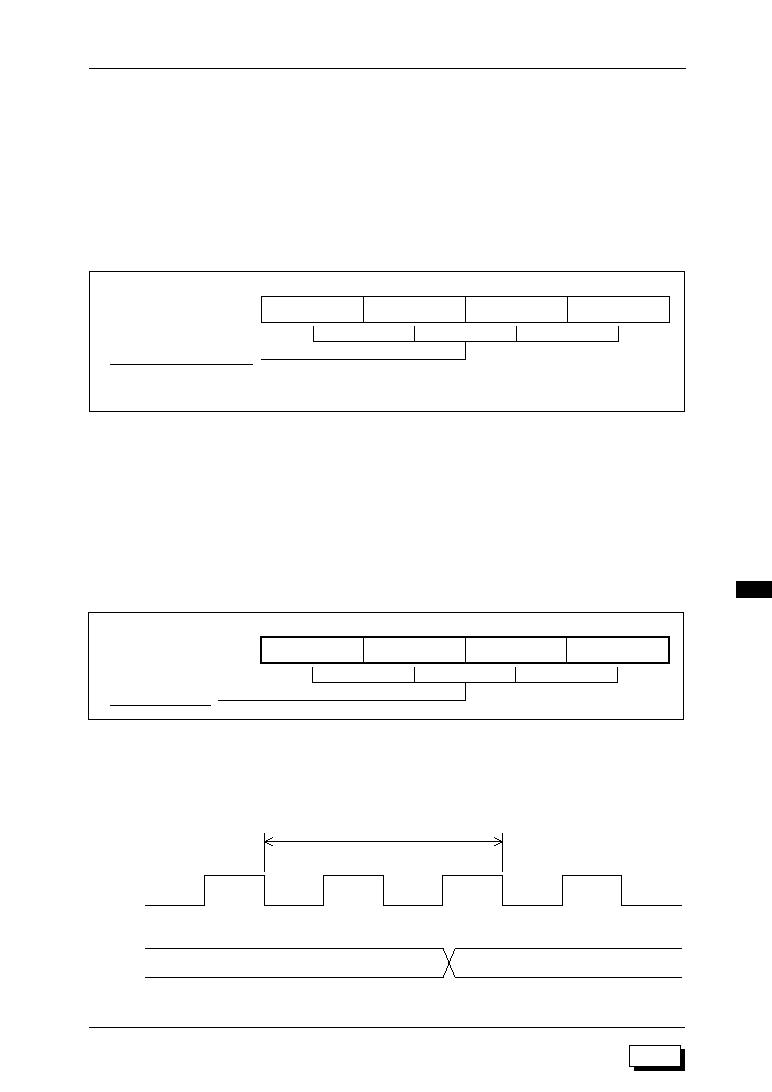
12-19
ML63187/189B/193 User's Manual
Chapter 12 Ports (INPUT, I/O PORT)
12
M187
M189B
M193
12.6.2 Port C Registers
(1) Port C direction register (PCDIR)
PCDIR is a 4-bit special function register (SFR) which specifies the port input/output direction
for each bit. Pins corresponding to PCDIR bits set to "0" are input, and those corresponding
to bits set to "1" are output.
At system reset all bits in the port C direction register are reset to "0", and port C is initialized
to input mode.
PC3DIR
PC2DIR
PC1DIR
PC0DIR
PCDIR (035H)
(R/W)
bit 3
bit 2
bit 1
bit 0
Port C input/output setting
0: Input (initial value)
1: Output
(2) Port C data register (PCD)
PCD is a 4-bit special function register used to set the output values for port C.
When a bit in the port C direction register (PCDIR) is set to "1" to select the output mode, the
content of the corresponding bit in the port C data register is output to the port C.
When a bit in the port C data register is read with the corresponding PCDIR bit set to output,
the value of the bit in the port C data register is read.
When a bit in the port C data register is read with the corresponding PCDIR bit set to "0" (input
mode), the level of the corresponding pin of port C is read.
PC3
PC2
PC1
PC0
PCD (00CH)
(R/W)
bit 3
bit 2
bit 1
bit 0
Port C output data
At system reset all bits in the port C data register (PCD) are set to "0". When data is written
to the port C data register, the actual pin change timing is at the rising edge of the system clock
for state 2 of the write instruction.
Figure 12-11 indicates port change timing.
S1
S2
Old data
New data
CLK
Port C
Write instruction
Figure 12-11 Port C Change Timing

12-20
ML63187/189B/193 User's Manual
Chapter 12 Ports (INPUT, I/O PORT)
M187
M189B
M193
(3) Port C control registers (PCCON0, PCCON1)
The port C control registers 0/1 (PCCON0, PCCON1) are 4-bit special function registers
(SFRs) used to select port input/output mode.
The input mode can be pull-down resistor input, pull-up resistor input or high-impedance
input.
The output mode can be CMOS output, N-channel open drain output, P-channel open drain
output or high-impedance output.
At system reset all bits in PCCON0 and PCCON1 are set to "0", and port C is initialized to
pull-down resistor input mode and CMOS output mode.
PC1MD1
PC1MD0
PC0MD1
PC0MD0
PCCON0 (033H)
(R/W)
bit 3
bit 2
bit 1
bit 0
Port C.1 input/output mode select
Input mode
bit 3
0
1
•
bit 2
0
0
1
: Input with pull-down resistor (initial value)
: Input with pull-up resistor
: High-impedance input
Port C.0 input/output mode select
Input mode
bit 1
0
1
•
bit 0
0
0
1
: Input with pull-down resistor (initial value)
: Input with pull-up resistor
: High-impedance input
Output mode
bit 3
0
0
1
1
bit 2
0
1
0
1
: CMOS output (initial value)
: N-channel open drain output
: P-channel open drain output
: High-impedance output
Output mode
bit 1
0
0
1
1
bit 0
0
1
0
1
: CMOS output (initial value)
: N-channel open drain output
: P-channel open drain output
: High-impedance output
PC3MD1
PC3MD0
PC2MD1
PC2MD0
PCCON1 (034H)
(R/W)
bit 3
bit 2
bit 1
bit 0
Port C.3 input/output mode select
Input mode
bit 3
0
1
•
bit 2
0
0
1
: Input with pull-down resistor (initial value)
: Input with pull-up resistor
: High-impedance input
Port C.2 input/output mode select
Input mode
bit 1
0
1
•
bit 0
0
0
1
: Input with pull-down resistor (initial value)
: Input with pull-up resistor
: High-impedance input
Output mode
bit 3
0
0
1
1
bit 2
0
1
0
1
: CMOS output (initial value)
: N-channel open drain output
: P-channel open drain output
: High-impedance output
Output mode
bit 1
0
0
1
1
bit 0
0
1
0
1
: CMOS output (initial value)
: N-channel open drain output
: P-channel open drain output
: High-impedance output
M193

12-21
ML63187/189B/193 User's Manual
Chapter 12 Ports (INPUT, I/O PORT)
12
M187
M189B
M193
(4) Port C mode registers (PCMOD0, PCMOD1)
The port C mode registers 0/1 (PCMOD0, PCMOD1) are 4-bit special function registers
(SFRs) used to select the sampling frequency when ports are used for external interrupt, and
to select secondary functions other than external interrupt.
The external interrupt sampling frequency is either 128 Hz or 4 kHz.
Port C secondary functions are indicated in Table 12-3.
Table 12-3 Port C Secondary Functions
Port
Secondary function
Description
PC.0
RXD
Serial port receive data input
PC.1
TXC
Serial port transmit clock I/O
PC.2
RXC
Serial port receive clock I/O
PC.3
TXD
Serial port transmit data output
PC.0
PC.1
PC.2
PC.3
INT1
External interrupt 1
12-22
ML63187/189B/193 User's Manual
Chapter 12 Ports (INPUT, I/O PORT)
M187
M189B
M193
--
--
--
PCF
PCMOD0 (037H)
(R/W)
External interrupt sampling frequency select
0: 128 Hz sampling (initial value)
1: 4 kHz sampling
bit 3
bit 2
bit 1
bit 0
PC3MOD
PC2MOD
PC1MOD
PC0MOD
PCMOD1 (038H)
(R/W)
bit 3
bit 2
bit 1
bit 0
Port C.3 pin function select
0: Input/output port function (initial value)
1: Serial port transmit data output (TXD) function (goes into output mode irrespective of PC3DIR)
Port C.2 pin function select
0: Input/output port function (initial value)
1: Serial port receive clock input/output (RXC) function (switching of input/output mode
depends on SRCLK bit of serial port receive control register SRCON1. It is performed irrespective of PC2DIR)
Port C.1 pin function select
0: Input/output port function (initial value)
1: Serial port transmit clock input/output (TXC) function (switching of input/output mode
depends on STCLK bit of serial port transmit control register STCON1. It is performed irrespective of PC1DIR)
Port C.0 pin function select
0: Input/output port function (initial value)
1: Serial port receive data input (RXD) function (goes into input mode irrespective of PC0DIR)
At system reset all the valid bits in the port C mode registers are initialized to "0".
M193

12-23
ML63187/189B/193 User's Manual
Chapter 12 Ports (INPUT, I/O PORT)
12
M187
M189B
M193
(5) Port C interrupt enable register (PCIE)
PCIE is a 4-bit special function register (SFR) that enables/disables individual bits when port
C is used as an external interrupt input.
At system reset, all bits in PCIE are cleared to "0" and port C is initialized to the interrupt
disabled state.
PC3IE
PC2IE
PC1IE
PC0IE
PCIE (036H)
(R/W)
bit 3
bit 2
bit 1
bit 0
Port C.3 interrupt enable/disable select
0: Interrupt disabled (initial value)
1: Interrupt enabled
Port C.2 interrupt enable/disable select
0: Interrupt disabled (initial value)
1: Interrupt enabled
Port C.1 interrupt enable/disable select
0: Interrupt disabled (initial value)
1: Interrupt enabled
Port C.0 interrupt enable/disable select
0: Interrupt disabled (initial value)
1: Interrupt enabled

12-24
ML63187/189B/193 User's Manual
Chapter 12 Ports (INPUT, I/O PORT)
M187
M189B
M193
12.6.3 Port C External Interrupt Function (External Interrupt 1)
Port C has external interrupt 1 allocated as secondary function. Individual bits of port C can
be enabled/disabled.
External interrupt generation for port C is triggered by the falling edge of the 128 Hz or 4 kHz
time base counter, which is the sampling clock.
After the port level changes, the interrupt request signal (XI1INT) is output, and the interrupt
request flag (QXI1) is set. The maximum delay for this sequence is one cycle of the sampling
clock (128 Hz or 4 kHz).
Because the port C external interrupt is set by a level change at any of the port C inputs, each
bit of the port must be read to determine which bit of port C generated the interrupt.
The interrupt start address for external interrupt 1 is 0016H.
Figure 12-12 shows the external interrupt 1 generation timing.
Figure 12-13 shows the equivalent circuit for external interrupt 1 control.
Level change
detect circuit
128 Hz
4 kHz
PCMOD0
PCF
PC0IE
PC1IE
PC2IE
PC3IE
PCIE
PC.0
PC.1
PC.2
PC.3
IE0.3
EXI1
to interrupt priority
encoder
IRQ0
IE0
IRQ0.3
QXI1
XI1INT
QXI1
(n = 0≠3)
XI1INT
PC.n
128 Hz or
4 kHz
Figure 12-12 External Interrupt 1 Generation Timing
Figure 12-13 External Interrupt 1 Control Equivalent Circuit
M193
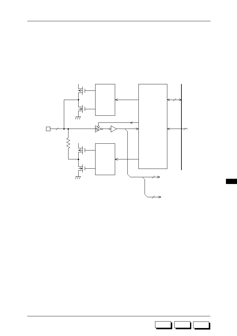
12-25
ML63187/189B/193 User's Manual
Chapter 12 Ports (INPUT, I/O PORT)
12
M187
M189B
M193
12.7 Port E (PE.0≠PE.3)
The ML63187, ML63189B, and ML63193 have Port E, a 4-bit input/output port.
12.7.1 Port E Configuration
The circuit configuration for port E is shown in Figure 12-14.
Figure 12-14 Input/Output Port (Port E) Configuration
Output
port
control
PED
PEDIR
PECON0
PECON1
PEMOD
Pull-up/
pull-down
control
4
2
V
DDI
V
DDI
PE.0≠PE.3
V
SS
V
SS
PE.3
(to external 2 interrupt
control circuit)
SOUT, SCLK
SIN, SCLK
(to shift register circuit)
1
2
(from shift
register
circuit)
4
Data bus

12-26
ML63187/189B/193 User's Manual
Chapter 12 Ports (INPUT, I/O PORT)
M187
M189B
M193
12.7.2 Port E Registers
(1) Port E direction register (PEDIR)
PEDIR is a 4-bit special function register (SFR) which specifies the port input/output direction
for each bit. Pins corresponding to PEDIR bits set to "0" are input, and those corresponding
to bits set to "1" are output.
At system reset all bits in the port E direction register are set to "0", and port E is initialized
to input mode.
PE3DIR
PE2DIR
PE1DIR
PE0DIR
PEDIR (03FH)
(R/W)
bit 3
bit 2
bit 1
bit 0
Port E input/output setting
0: Input (initial value)
1: Output
(2) Port E data register (PED)
PED is a 4-bit special function register used to set the output values for port E.
When a bit in the port E direction register (PEDIR) is set to "1" to select the output mode, the
content of the corresponding bit in the port E data register is output to the port E.
When a bit in the port E data register is read with the corresponding PEDIR bit set to output,
the value of the bit in the port E data register is read.
When a bit in the port E data register is read with the corresponding PEDIR bit set to "0" (input
mode), the level of the corresponding pin of port E is read.
PE3
PE2
PE1
PE0
PED (00EH)
(R/W)
bit 3
bit 2
bit 1
bit 0
Port E output data
At system reset all bits in the port E data register (PED) are reset to "0". When data is written
to the port E data register, the pin change timing is at the rising edge of the system clock for
state 2 of the write instruction.
Figure 12-15 indicates port change timing.
S1
S2
Old data
New data
CLK
Port E
Write instruction
Figure 12-15 Port E Change Timing

12-27
ML63187/189B/193 User's Manual
Chapter 12 Ports (INPUT, I/O PORT)
12
M187
M189B
M193
(3) Port E control registers (PECON0, PECON1)
The port E control registers 0/1 (PECON0, PECON1) are 4-bit special function registers
(SFRs) used to select port input/output mode.
The input mode can be pull-down resistor input, pull-up resistor input or high-impedance
input.
The output mode can be CMOS output, N-channel open drain output, P-channel open drain
output or high-impedance output.
At system reset all bits in PECON0 and PECON1 are set to "0", and port E is initialized to pull-
down resistor input mode and CMOS output mode.
PE1MD1
PE1MD0
PE0MD1
PE0MD0
PECON0 (03DH)
(R/W)
bit 3
bit 2
bit 1
bit 0
Port E.1 input/output mode select
Input mode
bit 3
0
1
•
bit 2
0
0
1
: Input with pull-down resistor (initial value)
: Input with pull-up resistor
: High-impedance input
Port E.0 input/output mode select
Input mode
bit 1
0
1
•
bit 0
0
0
1
: Input with pull-down resistor (initial value)
: Input with pull-up resistor
: High-impedance input
Output mode
bit 3
0
0
1
1
bit 2
0
1
0
1
: CMOS output (initial value)
: N-channel open drain output
: P-channel open drain output
: High-impedance output
Output mode
bit 1
0
0
1
1
bit 0
0
1
0
1
: CMOS output (initial value)
: N-channel open drain output
: P-channel open drain output
: High-impedance output
PE3MD1
PE3MD0
PE2MD1
PE2MD0
PECON1 (03EH)
(R/W)
bit 3
bit 2
bit 1
bit 0
Port E.3 input/output mode select
Input mode
bit 3
0
1
•
bit 2
0
0
1
: Input with pull-down resistor (initial value)
: Input with pull-up resistor
: High-impedance input
Port E.2 input/output mode select
Input mode
bit 1
0
1
•
bit 0
0
0
1
: Input with pull-down resistor (initial value)
: Input with pull-up resistor
: High-impedance input
Output mode
bit 3
0
0
1
1
bit 2
0
1
0
1
: CMOS output (initial value)
: N-channel open drain output
: P-channel open drain output
: High-impedance output
Output mode
bit 1
0
0
1
1
bit 0
0
1
0
1
: CMOS output (initial value)
: N-channel open drain output
: P-channel open drain output
: High-impedance output

12-28
ML63187/189B/193 User's Manual
Chapter 12 Ports (INPUT, I/O PORT)
M187
M189B
M193
(4) Port E mode register (PEMOD)
PEMOD is a 4-bit special function register (SFR) used to select the sampling frequency when
PE.3 is used as an external interrupt. It is also used to select port E secondary functions other
than external interrupt.
The external interrupt sampling frequency can be selected as either 128 Hz or 4 kHz.
Port E secondary functions are indicated in Table 12-4.
Table 12-4 Port E Secondary Functions
Port
Secondary function
Description
PE.0
SIN
Shift register data input
PE.1
SOUT
Shift register data output
PE.2
SCLK
Shift register clock I/O
PE.3
INT2
External interrupt 2
PEF
PE2MOD
PE1MOD
PE0MOD
PEMOD (040H)
(R/W)
bit 3
bit 2
bit 1
bit 0
External interrupt sampling frequency select
0: 128 Hz sampling (initial value)
1: 4 kHz sampling
Port E.1 pin function select
0: Input/output port function (initial value)
1: Shift register data output (SOUT) function (goes into output mode irrespective of PE1DIR)
Port E.2 pin function select
0: Input/output port function (initial value)
1: Shift register clock input/output (SCLK) function
(Switching of input/output mode depends on the input/output selection of
the shift clock of the shift register control register SFTCON0, irrespective
of the PE2DIR value.)
Port E.0 pin function select
0: Input/output port function (initial value)
1: Shift register data input (SIN) function (goes into input mode irrespective of PE0DIR)
At system reset all bits in PEMOD are initialized to "0".

12-29
ML63187/189B/193 User's Manual
Chapter 12 Ports (INPUT, I/O PORT)
12
M187
M189B
M193
12.7.3 Port E.3 External Interrupt Function (External Interrupt 2)
Port E.3 has external interrupt 2 allocated as secondary function.
External interrupt generation for PE.3 is triggered by the falling edge of the 128 Hz or 4 kHz
time base counter, which is the sampling clock.
After the port level changes, the interrupt request signal (XI2INT) is output, and the interrupt
request flag (QXI2) is set. The maximum delay for this sequence is one cycle of the sampling
clock (128 Hz or 4 kHz).
The interrupt start address for external interrupt 2 is 0018H.
Figure 12-16 shows the external interrupt 2 generation timing.
Figure 12-17 shows the equivalent circuit for external interrupt 2 control.
QXI2
XI2INT
PE.3
128 Hz or
4 kHz
Figure 12-16 External Interrupt 2 Generation Timing
Figure 12-17 External Interrupt 2 Control Equivalent Circuit
Level change
detect circuit
128 Hz
4 kHz
PEMOD
PEF
IE1.0
IE1
EXI2
to interrupt priority
encoder
IRQ1.0
IRQ1
QXI2
XI2INT
PE.3

12-30
ML63187/189B/193 User's Manual
Chapter 12 Ports (INPUT, I/O PORT)
M187
M189B
M193

M189B
M187
M193
Chapter 13
13
Melody Driver (MELODY)

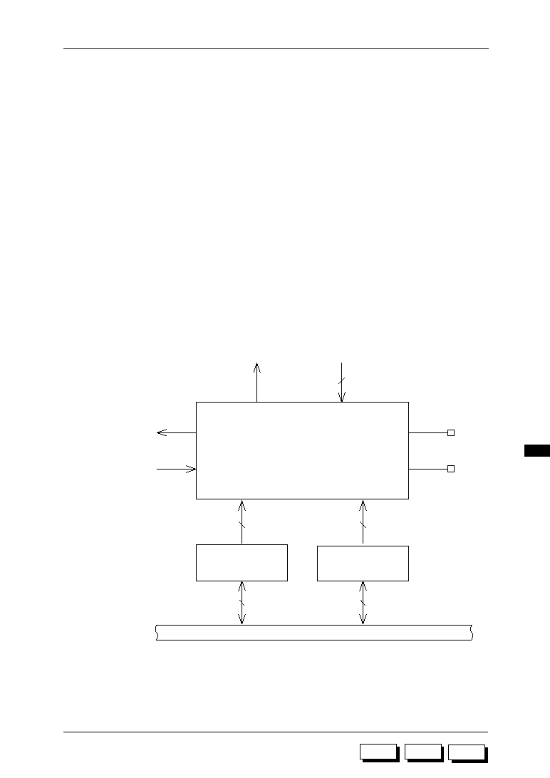
13-1
ML63187/189B/193 User's Manual
Chapter 13 Melody Driver (MELODY)
13
M187
M189B
M193
Chapter 13 Melody Driver (MELODY)
13.1 Overview
The ML63187, ML63189B, and ML63193 have an internal melody circuit and buzzer circuit.
While automatically reading melody data in ROM (program memory) as specified by an MSA
instruction, the melody circuit outputs a melody signal via the MD and MDB pins.
The melody circuit can select 29 different tones, 63 different tone lengths, and 15 different
tempos.
The buzzer circuit has four different buzzer output modes at a frequency of 4 kHz. The buzzer
driver signal is output via the MD and MDB pins.
Melody output is a higher priority operation than buzzer output.
13.2 Melody Driver Configuration
The melody driver configuration is shown in Figure 13-1.
Data bus
Melody end interrupt
request
MSA instruction
Melody data request
Melody data
MD
MDB
14
TEMPO
MDCON
Melody circuit
Buzzer circuit
4
4
4
4
Figure 13-1 Melody Driver Configuration

13-2
ML63187/189B/193 User's Manual
Chapter 13 Melody Driver (MELODY)
M187
M189B
M193
13.3 Melody Driver Registers
(1) Tempo Register (TEMPO)
TEMPO is a 4-bit special function register (SFR) that sets the tempo of the melody driver.
(2) Melody Driver Control Register (MDCON)
MDCON is a 4-bit special function register (SFR) that controls output of the melody driver.
TMP3
TMP2
TMP1
TMP0
TEMPO (096H)
(R/W)
bit 3
bit 2
bit 1
bit 0
Melody tempo select
bit 3
0
0
0
0
0
0
0
0
1
1
1
1
1
1
1
1
bit 2
0
0
0
0
1
1
1
1
0
0
0
0
1
1
1
1
bit 1
0
0
1
1
0
0
1
1
0
0
1
1
0
0
1
1
bit 0
0
1
0
1
0
1
0
1
0
1
0
1
0
1
0
1
: = 480 (initial value)
: = 480
: = 320
: = 240
: = 192
: = 160
: = 137
: = 120
: = 107
: = 96
: = 87
: = 80
: = 74
: = 69
: = 64
: = 60
MSF
EMBD
MBM1
MBM0
MDCON (097H)
(R/W)
bit 3
bit 2
bit 1
bit 0
Melody status flag
0 : Melody stopped (initial value)
1 : Melody output
Buzzer output ON/OFF control
0 : Buzzer output OFF (initial value)
1 : Buzzer output ON
Buzzer mode select
bit 1
0
0
1
1
bit 0
0
1
0
1
: Intermittent tone 1 (initial value)
: Intermittent tone 2
: Single tone
: Continuous tone

13-3
ML63187/189B/193 User's Manual
Chapter 13 Melody Driver (MELODY)
13
M187
M189B
M193
bit 3: MSF
This flag indicates the melody output status.
When an MSA instruction starts the melody, MSF is set to "1". After output of the
last melody data (END bit is "1"), MSF is cleared to "0".
Setting MSF to "0" during melody output will forcibly stop the melody output. If
forcibly stopped, the melody output cannot be restarted at the address at which
it was stopped.
At system reset, MSF is cleared to "0".
!
Note:
If MSF (bit 3 of MDCON) is set to "0" to stop melody output forcibly, it is required to set the
stop address on the ROM table to the end-data address (8000H). In this case, set MSF to
"0" after writing the melody end data that consists of two words of melody (silence with the
END bit being "1") data. If this programming is not executed, melody output may not be
stopped even if MSF is set to "0". Example programming is shown below.
;*Program part***********
DI
; 0. Disable master interrupt (MIE).
MSA MDSTOP_DATA
; 1. Write melody end data to the melody circuit.
MOV A,#0
; 2. Set the MSF to "0".
MOV MDCON,A
;
MOV A,#1101b
; 3. Clear melody end interrupt request (QMD).
AND IRQ0,A
;
EI
; 4. Enable master interrupt (MIE).
;*ROM table data part****
;*Provide two words of melody data so that a melody will always be terminated even if a melody
;*request is issued twice.
MDSTOP_DATA:
DW
8000H
; Silence data 1
DW
8000H
; Silence data 2
;************************
The Development Support System (EASE63180 Emulator) differs from the IC in actual
operation: In the EASE63180 Emulator, melody output will be stopped only by setting MSF
to "0"; writing melody end data is not needed.
bit 2: EMBD
This bit turns the buzzer output ON or OFF.
At system reset, EMBD is cleared to "0" and buzzer output is turned OFF.
In the single tone output mode, setting EMBD to "1" turns ON the buzzer output.
After the second falling edge of the 32 Hz output, EMBD is cleared to "0" and
buzzer output is turned OFF.
If melody output is started during buzzer output, EMBD is cleared to "0" and the
buzzer output is turned OFF.
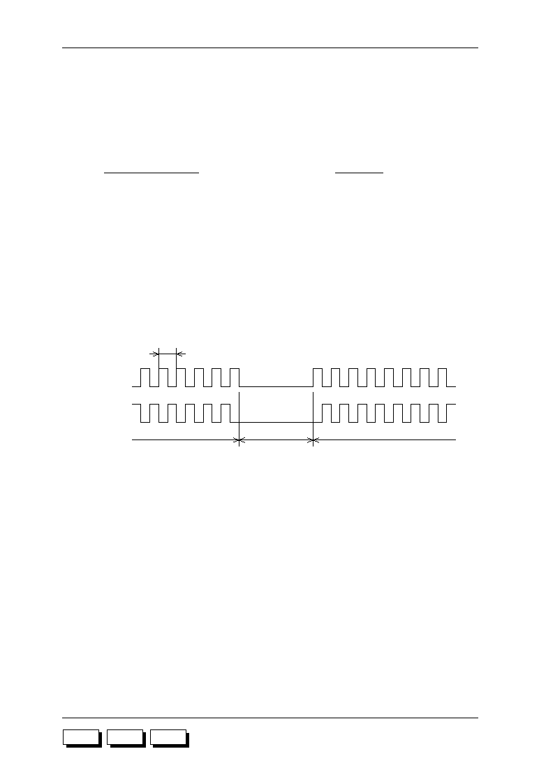
13-4
ML63187/189B/193 User's Manual
Chapter 13 Melody Driver (MELODY)
M187
M189B
M193
13.4 Melody Circuit Operation
After the melody tempo is set in the tempo register (TEMP), execution of an MSA instruction
will start operation of the melody circuit.
The melody circuit outputs melody data while automatically reading melody data in ROM
(program memory) as specified by an MSA instruction. When the last melody data is read
(END bit is "1"), the melody circuit generates a melody end interrupt request. At this time, if
an MSA instruction is executed, after the last melody data is output, melody output will
continue from the melody data specified by the MSA instruction. If an MSA instruction is not
executed, the melody output will stop after the last melody data is output.
MSF (bit 3 of MDCON) is a flag indicating the melody output status. When MSF is "1", the
melody is being output, and when "0", the melody is stopped. Setting MSF to "0" during
melody output will forcibly stop the melody output. If it is required to stop melody output
forcibly, describe the program according to the "Note" on page 13-3. If forcibly stopped, the
melody output cannot be restarted at the address at which it was stopped.
bit 1, 0: MBM1, MBM0
These bits select the buzzer output mode.
Output of two types of intermittent tones, a single tone or a continuous tone can
be selected.
At system reset, MBM1 and MBM0 are cleared to "0", selecting output of
intermittent tone 1.
Buzzer output mode
Waveform
Intermittent tone 1
Intermittent tone waveform synchronized to 8 Hz
output of time base counter
Intermittent tone 2
Intermittent tone waveform synchronized to the logical
AND of 8 Hz signal output and a "L" level of 1 Hz
signal output of the time base counter
Single tone
Single tone waveform beginning when EMBD is set
to "1" until second falling edge of 32 Hz output of time
base counter
Continuous tone
Continuous tone waveform that is constant while
EMBD is "1"
Figure 13-2 shows the output waveforms of the melody driver output pins.
Cycle specified by tone code
MD output
MDB output
Output state
No output state
Output state
Figure 13-2 Output Waveforms of Melody Driver Output Pins

13-5
ML63187/189B/193 User's Manual
Chapter 13 Melody Driver (MELODY)
13
M187
M189B
M193
13.4.1 Tempo Data
Tempo data defines the basic tone length. Tempo data is set in the tempo register (TEMPO).
The tempos (number of counts per minute) set by TEMPO are shown in Table 13-1.
Table 13-1 Melody Tempo
0H
1H
2H
3H
5H
6H
7H
8H
9H
AH
BH
CH
DH
EH
FH
0
0
0
0
0
0
0
0
0
0
0
0
0
0
0
1
0
0
0
0
0
0
0
0
0
0
0
1
1
0
0
1
1
1
1
1
1
1
1
1
0
1
1
1
1
1
1
1
1
1
1
1
1
1
1
1
1
1
1
1
= 480
= 480
= 320
= 240
= 160
137
= 120
107
= 96
87
= 80
74
69
= 64
= 60
TP3
TP2
TP1
TP0
TEMPO
Tempo
4H
0
1
0
0
= 192
TP3≠0
=
=
=
=
=
13-6
ML63187/189B/193 User's Manual
Chapter 13 Melody Driver (MELODY)
M187
M189B
M193
Figure 13-3 Melody Data Format
(1) Tone code
The tone code is set in bits 6 through 0 of the melody data. The frequencies that
can be output by the melody circuit are defined as:
65536
(N + 2)
The relation between N and tone code bits is:
N = 2
6
N6 + 2
5
N5 + 2
4
N4 + 2
3
N3 + 2
2
N2 + 2
1
N1 + 2
0
N0
If N6 through N2 are all set to "0", there is no melody output for the time specified
by the tone length code. Values for N1 and N0 are irrelevant.
Table 13-2 indicates the relations between tones and tone codes.
Table 13-2 Tone and Tone Code Correspondence
13.4.2 Melody Data
Melody data is 14-bit format data in the program ROM defining tone, tone length and end tone.
The melody data format is indicated in Figure 13-3.
N0
N1
N2
N3
END --*
L5
L4
L3
L2
L1
L0
--*
N6
N5
N4
bit 0
bit 1
bit 2
bit 3
bit 4
bit 5
bit 6
bit 7
bit 8
bit 9
bit 10
bit 11
bit 12
bit 13
bit 14
bit 15
End bit
Tone length code
Tone code
* Bits 14 and 7 may be either "0" or "1".
Tone
Frequency
(Hz)
Tone code
N6
N5
N4
N3
N2
N1
N0
N6≠N0
Gis
1
A
1
Ais
1
B
1
C
2
Cis
2
D
2
840
886
936
993
1192
1111
1057
1
1
1
1
1
1
1
1
1
1
0
0
0
0
0
0
0
0
0
0
0
0
0
0
0
0
0
1
1
1
1
1
1
1
1
0
0
0
0
0
0
0
0
0
0
0
1
0
1
4CH
48H
44H
40H
3CH
39H
35H
C
1
529
1
1
1
1
0
1
1
7BH
Cis
1
560
1
1
1
0
0
1
1
73H
D
1
590
1
1
0
1
1
0
1
6DH
Dis
1
624
1
1
0
0
1
1
1
67H
E
1
662
1
1
0
0
0
0
1
61H
F
1
705
0
1
1
1
0
1
1
5BH
Fis
1
745
0
1
1
0
1
1
0
56H
G
1
790
0
1
1
0
0
0
1
51H
Hz (where N is an integer from 4 to 127)

13-7
ML63187/189B/193 User's Manual
Chapter 13 Melody Driver (MELODY)
13
M187
M189B
M193
Table 13-2 Tone and Tone Code Correspondence (continued)
Tone
Frequency
(Hz)
Tone code
N6
N5
N4
N3
N2
N1
N0
N6≠N0
Gis
2
A
2
Ais
2
B
2
C
3
D
3
Dis
3
E
3
Fis
3
1680
1771
1872
2979
2621
2521
2341
2114
1986
0
0
0
0
0
1
1
0
1
0
1
0
0
1
1
0
0
0
0
0
0
1
0
1
0
1
0
0
0
1
0
1
1
1
0
1
0
0
1
0
1
1
1
0
0
0
1
1
1
0
1
1
1
0
1
1
0
1
1
0
0
0
0
25H
23H
21H
1FH
1DH
1AH
18H
17H
14H
G
2
1560
0
1
0
1
0
0
0
28H
Dis
2
E
2
F
2
Fis
2
1490
1394
1338
1260
1
1
1
1
1
0
0
0
0
0
0
0
0
0
1
1
0
1
1
1
1
1
1
1
0
0
1
0
32H
2FH
2DH
2AH
(2) Tone length code
The tone length code is set in melody data bits 13 through 8.
Table 13-3 indicates the relation between tone length and tone length code (L5 to L0).
The tone length that is set during execution of the MSA instruction is shorter by approximately
1 to 3 ms.
When all bits are set to "0", the tone length will be the same as the minimum tone length (the
tone length with only L0 set to "1").

13-8
ML63187/189B/193 User's Manual
Chapter 13 Melody Driver (MELODY)
M187
M189B
M193
Table 13-3 Tone Length and Tone Length Code Correspondence
Tone length code
L5
L4
L3
L2
L1
L0
Tone
length
L5≠L0
1
1
1
1
1
1
3FH
1
0
1
1
1
1
2FH
0
1
1
1
1
1
1FH
0
1
0
1
1
1
17H
0
0
1
1
1
1
0FH
0
0
1
0
1
1
0BH
0
0
0
1
1
1
07H
0
0
0
1
0
1
05H
0
0
0
0
1
1
03H
0
0
0
0
1
0
02H
0
0
0
0
0
1
01H
Tone lengths specified by the tone length code and the tempo data are expressed by the
following:
1.953125
•
(TP + 1)
•
(L + 1) ms
(where TP is an integer from 1 to 15, and L is
an integer from 1 to 63)
TP is a value set in the tempo register (TEMPO), and has the following bit correspondence:
TP = 2
3
TP3 + 2
2
TP2 + 2
1
TP1 + 2
0
TP0
L is set by the tone length code, and has a bit correspondence with the tone length code as:
L = 2
5
L5 + 2
4
L4 + 2
3
L3 + 2
2
L2 + 2
1
L1 + 2
0
L0
(3) END bit
The END bit is set in bit 15 of the melody data. When the output of the last melody data is
started (END bit is "1"), the melody circuit generates a melody end interrupt request, and
stops the melody after the last melody data is output.

13-9
ML63187/189B/193 User's Manual
Chapter 13 Melody Driver (MELODY)
13
M187
M189B
M193
13.4.3 Melody Circuit Application Example
An example melody is shown in Figure 13-4.
Table 13-4 lists the note codes for the melody shown in Figure 13-4.
15
14
13
12
11
10
END --*
L5
L4
L3
L2
9
8
7
L1
L0
--*
6
5
4
3
2
1
N6
N5
N4
N3
N2
N1
0
N0
Hex
0
0
0
2F28H
1
0
1
0
0
1
1
1
1
0
1
0
0
0
0
0
1
0
1
0
0
1
1
1
1
1
0
1
0
0F35H
0F28H
0
0
0
1
0
1
0
0
1
1
1
1
0
0
0
0
0
0
0
0
1
0
1
0
0
1
1
0
1
0
1
1
0735H
0F28H
0
0
0
1
0
1
0
0
1
1
1
0
0
1
0
0
0
0
0
0
0
1
0
0
1
1
1
0
0
0
1
1
1
0
0
1
1
0
0
0
1
1
1
1
1
1
1
1
1
0
1
1
1
1
0
0
1
1
1
0
0
1
0
0
0723H
3F1FH
BF28H
Note code
Note
G2
D2
G2
D2
G2
0700H
0
0
0
0
0
0
0
0
1
1
1
0
0
0
0
0
0700H
0
0
0
0
0
0
0
0
1
1
1
0
0
0
1
0
--
--
A2
B2
G2
Figure 13-4 Example Melody
Table 13-4 Note Code Table
4
= 120
4
* Bits 14 and 7 may be "0" or "1", but in this example they are shown as "0".

13-10
ML63187/189B/193 User's Manual
Chapter 13 Melody Driver (MELODY)
M187
M189B
M193
13.5 Buzzer Circuit Operation
When EMBD (bit 2 of MDCON) is set to "1", a buzzer driver signal is sent to the melody driver
output pins (MD, MDB).
Four buzzer output modes can be selected by MBM1 (bit 1 of MDCON) and MBM0 (bit 0 of
MDCON): two types of intermittent tones, a single tone, or a continuous tone output. The
buzzer output frequency is 4 kHz and has a 50% duty ratio.
In the intermittent tone 1 mode, a waveform synchronized to the 8 Hz output of the time base
counter is output.
In the intermittent tone 2 mode, a waveform synchronized to the logical AND of 8 Hz signal
output and a "L" level of 1 Hz signal of the time base counter is output.
In the single tone mode, output starts in synchronization with the rising edge of EMBD. At the
second falling edge of the 32 Hz output of the time base counter, EMBD is cleared to "0" and
output is stopped.
In the continuous tone mode, output is continued while EMBD is "1".
While the melody is being output (MSF (bit 3 of MDCON) = "1"), the buzzer output is turned
OFF. If melody output is started during buzzer output, EMBD is cleared to "0", the buzzer
output is stopped, and melody output is given priority.
Figure 13-5 shows the output waveforms of each mode. Shaded sections indicate the 4 kHz
output frequency.
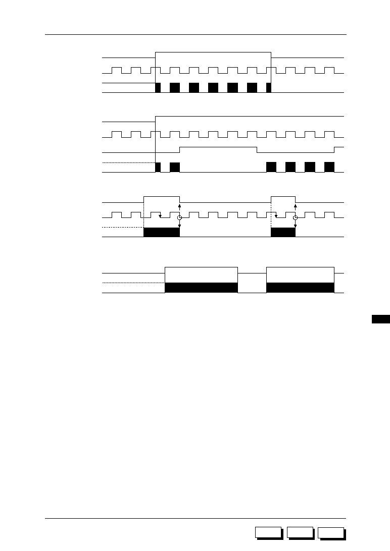
13-11
ML63187/189B/193 User's Manual
Chapter 13 Melody Driver (MELODY)
13
M187
M189B
M193
Figure 13-5 Buzzer Driver Output Waveforms in Each Output Mode
EMBD
8 Hz
Output MD
ON
OFF
(a) MBM1 = 0, MBM0 = 0 (intermittent tone 1)
EMBD
8 Hz
Output MD
ON
OFF
1 Hz
EMBD
32 Hz
Output MD
ON
OFF
EMBD
Output MD
ON
OFF
(b) MBM1 = 0, MBM0 = 1 (intermittent tone 2)
(c) MBM1 = 1, MBM0 = 0 (single tone)
(d) MBM1 = 1, MBM0 = 1 (continuous tone)

13-12
ML63187/189B/193 User's Manual
Chapter 13 Melody Driver (MELODY)
M187
M189B
M193

M193
Chapter 14
14
Serial Port (SIO)


14-1
ML63187/189B/193 User's Manual
Chapter 14 Serial Port (SIO)
14
M193
Chapter 14 Serial Port (SIO)
14.1 Overview
The ML63193 has a built-in serial communication port (serial port) for either synchronous or
asynchronous communication.
The serial port implements the send and receive circuits in independent circuits, making it
possible to send and receive simultaneously.
The send and receive modes can be UART mode (asynchronous communication mode) or
synchronous mode (synchronous communication mode).
In synchronous mode an internal clock mode generates the shift clock internally, and an
external clock mode receives an external shift clock.
Table 14-1 shows the serial port modes.
Table 14-1 Serial Port Modes
Mode
Baud rate
UART mode
Can be set to a user-specified value
with timers 2, 3 (TM2, 3)
Synchronous
mode
32.768 kHz
From external clock
∑ 9600 bps
UART mode
∑ 4800 bps
∑ 2800 bps
∑ 1200 bps
From external clock
32.768 kHz
Internal clock mode
External clock mode
Synchronous
mode
Internal clock mode
External clock mode
Receive side
Send side
Serial port
14.2 Serial Port Configuration
Figure 14-1 indicates the serial port configuration.
The serial port consists of the send/receive clock generator circuits, the send/receive control
registers, the buffer registers to store send/receive data, send/receive data transfer shift
registers, and the send/receive status registers.
PC.0/RXD is the send serial data input pin, PC.3/TXD is the send serial data output pin, PC.1/
TXC is the serial send clock I/O pin, and PC.2/RXC is the serial receive clock I/O pin. Set I/
O and secondary functions with the port control registers as needed for each communication
mode.

14-2
ML63187/189B/193 User's Manual
Chapter 14 Serial Port (SIO)
M193
DIR
DIR
Status register
Baud rate select
register
Transmitter
shift clock
generator
Receiver
shift clock
generator
STINT (to interrupt)
TM3INT (from timers 2, 3)
SRINT (to interrupt)
PC.2/RXC
PC.1/TXC
PC.0/RXD
PC.3/TXD
RXCI
RXCO
TXCI
TXCO
Transmitter
RXD
RXCO
BRTC
Receiver
32 kHz
RXCI
32 kHz
(0ACH)
SRBRT
(0AAH)
SRCON0
(0ABH)
SRCON1
(0A9H)
SRBUFH
(0A8H)
SRBUFL
(0ADH)
SSTAT
(0A5H)
STBUFH
(0A4H)
STBUFL
(0A6H)
STCON0
(0A7H)
STCON1
BFULL
OERR
PERR
FERR
Data bus
Inside the IC
Receive control
register
Receive buffer
register
LSB/MSB
select
LSB/MSB
select
Receive register
Send register
Send buffer register
Send control register
Figure 14-1 Serial Port Configuration

14-3
ML63187/189B/193 User's Manual
Chapter 14 Serial Port (SIO)
14
M193
STSTB
STL1
STL0
STMOD
Stop bit length select
0: 1 stop bit (initial value)
1: 2 stop bits
Send data length select
bit 2 bit 1 Data length
0 0 : 5 bits (initial value)
0 1 : 6 bits
1 0 : 7 bits
1 1 : 8 bits
Send mode selct
0 : UART mode (initial value)
1 : Synchronous mode
STCON0 (0A6H)
(R/W)
bit 3
bit 2
bit 1
bit 0
bit 3: STSTB (Serial Transmission STop Bit)
This bit specifies stop bit length. Valid only when bit 0 is "0" (UART mode).
bit 2, 1: STL1 (Serial Transmission Length select bit 1),
STL0 (Serial Transmission Length select bit 0)
These bits specify the send data length.
bit 0: STMOD (Serial Transmission MODe bit)
This bit specifies the serial port send operation mode.
14.3 Serial Port Registers
(1) Send control registers 0/1 (STCON0, STCON1)
STCON0 and STCON1 are 4-bit special function registers (SFRs) to control the serial port
send operation. STCON0 and STCON1 are initialized to "0" at system reset.

14-4
ML63187/189B/193 User's Manual
Chapter 14 Serial Port (SIO)
M193
STLMB
STPOE
STPEN
STCLK
LSB/MSB head select
0 : Start from LSB (initial value)
1 : Start from MSB
Odd/even parity select
0 : Odd parity (initial value)
1 : Even parity
Parity set
0 : No parity bit (initial value)
1 : Parity bit
Send external/internal clock select
0 : External clock mode (initial value)
1 : Internal clock mode
STCON1 (0A7H)
(R/W)
bit 3
bit 2
bit 1
bit 0
bit 3: STLMB (Serial Transmission Least significant bit first or Most significant Bit first)
This bit specifies either LSB first or MSB first for send data.
bit 2: STPOE (Serial Transmission Parity Odd or Even number bit)
This bit specifies whether the parity bit is even or odd. Valid only when bit 1 is "1"
(parity bit).
bit 1: STPEN (Serial Transmission Parity ENable bit)
This bit specifies whether or not a parity bit is added.
bit 0: STCLK (Serial Transmission CLock select bit)
This bit specifies the external/internal send clock for synchronous mode. Valid
only when STMOD (bit 0 of STCON0) is "1" (synchronous mode).

14-5
ML63187/189B/193 User's Manual
Chapter 14 Serial Port (SIO)
14
M193
(2) Send buffer registers (STBUFL, STBUFH)
STBUFL and STBUFH are 4-bit special function registers (SFRs) that set send data for serial
port send operation.
LSB/MSB selection (described later) allows the data send direction (LSB or MSB first) to be
specified. Both STBUFL and STBUFH are initialized to "0" at system reset.
Send operation begins when send data is set to STBUFH. Be sure to set send data to
STBUFL before setting data to STBUFH.
Also set the baud rate and send mode before beginning send operation.
If send operation is already under way when send data is set to STBUFH, send for the new
data begins when the prior send has ended, and at the same time an interrupt request signal
(STINT) is generated. In the STINT interrupt routine the program should first write the send
data to STBUFL and STBUFH to assure no pauses in the send sequence.
(3) Send register
The send register is a shift register that handles the shift operation in send. At system reset
it is cleared to 00H. The send register cannot be directly accessed from the CPU.
The hardware send flow is indicated in Figure 14-2, to explain the timing for transfer of data
from STBUFL/H to the send register.
First set the send mode and baud rate. When send data is set to STBUFH, the status (SSTAT)
buffer full flag (BFULL) is set to "1", and unless send operation is already under way the
content of STBUFL/H is transferred to the send register and send operation begins. When
send operation begins the BFULL flag is reset to "0", and the next send data can be set to
STBUFL/H.
If prior data send operation is not complete, the send data is held in STBUFL/H until send is
completed. In this case BFULL remains set to "1". When the prior send operation is complete
the send data will be transferred from STBUFL/H to the send register, and send begins.
!
Note:
When BFULL is "1" it is possible to set data to STBUFL/H, but prior data set to STBUFL/H
that is being held there is overwritten and lost. Always set data after verifying that the BFULL
flag is "0".
TB3
TB2
TB1
TB0
STBUFL (0A4H)
(R/W)
bit 3
bit 2
bit 1
bit 0
TB7
TB6
TB5
TB4
STBUFH (0A5H)
(R/W)
bit 3
bit 2
bit 1
bit 0

14-6
ML63187/189B/193 User's Manual
Chapter 14 Serial Port (SIO)
M193
START
Write send data to
STBUFH ?
BFULL
®"1"
Sending?
STBUFL/H to send register
BFULL
®"0"
Start send
STINT generated
No
Yes
No
Yes
Figure 14-2 Hardware Send Operation Flow

14-7
ML63187/189B/193 User's Manual
Chapter 14 Serial Port (SIO)
14
M193
(4) Receive control registers 0/1 (SRCON0, SRCON1)
SRCON0 and SRCON1 are 4-bit special function registers (SFRs) controlling serial port
receive operation.
SRCON0 and SRCON1 are initialized to "0" at system reset.
SREN
SRL1
SRL0
SRMOD
Receive disable/enable select
0 : Receive disable (initial value)
1 : Receive enable
Receive data length select
bit 2 bit 1 Data length
0 0 : 5 bits (initial value)
0 1 : 6 bits
1 0 : 7 bits
1 1 : 8 bits
Receive mode select
0 : UART mode (initial value)
1 : Synchronous mode
SRCON0 (0AAH)
(R/W)
bit 3
bit 2
bit 1
bit 0
bit 3: SREN (Serial Reception ENable bit)
This bit specifies receive operation disable/enable. After receive is enabled in the
synchronous mode, this bit is reset to "0" after receiving one frame of data. In the
UART mode it does not change.
bit 2, 1: SRL1 (Serial Reception Length select bit 1),
SRL0 (Serial Reception Length select bit 0)
These bits specify the receive data length.
bit 0: SRMOD (Serial Reception MODe bit)
This bit specifies the serial port receive operation mode.
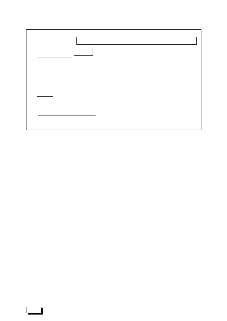
14-8
ML63187/189B/193 User's Manual
Chapter 14 Serial Port (SIO)
M193
SRLMB
SRPOE
SRPEN
SRCLK
LSB/MSB head select
0 : Start at LSB (initial value)
1 : Start at MSB
Odd/even parity select
0 : Odd parity (initial value)
1 : Even parity
Parity set
0 : No parity bit (initial value)
1 : Parity bit
Receive external/internal clock select
0 : External clock mode (initial value)
1 : Internal clock mode
SRCON1 (0ABH)
(R/W)
bit 3
bit 2
bit 1
bit 0
bit 3: SRLMB (Serial Reception Least significant bit first or Most significant Bit first)
This bit specifies either LSB first or MSB first for receive data.
bit 2: SRPOE (Serial Reception Parity Odd or Even number bit)
This bit specifies whether the parity bit is even or odd. Valid only when bit 1 is "1"
(parity bit).
bit 1: SRPEN (Serial Reception Parity ENable bit)
This bit specifies whether or not a parity bit is added.
bit 0: SRCLK (Serial Reception CLocK select bit)
This bit specifies the external/internal receive clock for synchronous mode. Valid
only when SRMOD (bit 0 of SRCON0) is "1" (synchronous mode).
14-9
ML63187/189B/193 User's Manual
Chapter 14 Serial Port (SIO)
14
M193
SRBUFL and SRBUFH are 4-bit special function registers (SFRs) used to hold the received
data in serial port reception. SRBUFL and SRBUFH are initialized to "0" at system reset.
When receive operation is completed the contents of the receive register are sent to SRBUFL/
H, and the receive interrupt request (SRINT) is generated. The contents of SRBUFL/H are
held until the next receive operation is completed.
If data from a prior receive operation is in SRBUFL/H and new data is received, an overrun
error will result. When an overrun error is generated, new received data cannot be loaded into
SRBUFL/H.
(5) Receive register
The receive register is the shift register that handles shift operation at receive. It is initialized
to 00H at system reset. It cannot be directly accessed by the CPU. When a receive operation
is complete, the data read into the receive register is transferred to SRBUFL/H, and at the
same time the receive interrupt request signal (SRINT) is generated.
(6) Receive buffer registers (SRBUFL, SRBUFH)
RB3
RB2
RB1
RB0
SRBUFL (0A8H)
(R)
bit 3
bit 2
bit 1
bit 0
RB7
RB6
RB5
RB4
SRBUFH (0A9H)
(R)
bit 3
bit 2
bit 1
bit 0
14-10
ML63187/189B/193 User's Manual
Chapter 14 Serial Port (SIO)
M193
(7) Receive baud rate setting register (SRBRT)
SRBRT is a 4-bit special function register (SFR) used to set the receive baud rate for serial
port receive operation in UART mode.
SRBRT is initialized to 0CH at system reset.
--
--
BRT1
BRT0
Receive baud rate setting
bit 1 bit 0 Baud rate
0 0 : 1200 bps (initial value)
0 1 : 2400 bps
1 0 : 4800 bps
1 1 : 9600 bps
SRBRT (0ACH)
(R/W)
bit 3
bit 2
bit 1
bit 0
bit 1, 0: BRT1 (Baud RaTe select bit1), BRT0 (Baud RaTe select bit 0)
These bits set the receive baud rate.

14-11
ML63187/189B/193 User's Manual
Chapter 14 Serial Port (SIO)
14
M193
(8) Serial status register (SSTAT)
SSTAT is a 4-bit special function register (SFR) used to indicate the status of serial port send/
receive.
SSTAT is initialized to "0" at system reset.
SSTAT is a read-only register, and the content is reset every time it is read.
bit 3: BFULL (send Buffer FULL flag)
This bit is enabled in both UART and synchronous modes, and is set to "1" when
send data is set to STBUFL/H in the send mode, and reset to "0" when the send
data is transferred to the send register.
When BFULL is set to "1" and send data is set (written) to STBUFL/H, the previous
data set to those registers is overwritten and lost. Always set data only after
verifying that the BFULL flag is "0".
bit 2: PERR (Parity ERRor flag)
This bit is enabled in both UART and synchronous modes, and is set to "1" when
the parity for the received data does not match the parity bit attached to the data.
bit 1: OERR (Overrun ERRor flag)
This bit is enabled in both UART and synchronous modes, and is set to "1" when
data reception is completed and the data received the previous time has still not
been transferred to the CPU. In this case, the new data cannot be transferred to
SRBUFL/H.
bit 0: FERR (Framing ERRor flag)
This is only enabled in the UART mode and is set to "1" in the following instances.
(1) when a "1" is detected in start bit sampling
(2) when a "0" is detected in stop bit sampling
In either case a receive interrupt request signal (SRINT) is generated.
BFULL
PERR
OERR
FERR
Send buffer status flag
0 : Send buffer empty (initial value)
1 : Send buffer full
Parity error flag
0 : No parity error (initial value)
1 : Parity error
Overrun flag
0 : No overrun error (initial value)
1 : Overrun error
Framing error
0 : No framing error (initial value)
1 : Framing error
SSTAT (0ADH)
(R)
bit 3
bit 2
bit 1
bit 0

14-12
ML63187/189B/193 User's Manual
Chapter 14 Serial Port (SIO)
M193
14.4 Serial Port Operation Description
14.4.1 Data Format
(1) UART mode
The data format for the UART mode is shown in Figure 14-3.
SRCON0/1 and STCON0/1 can be set to specify a data bit length of 5 to 8 bits.
The parity bit can be enabled/disabled. If enabled it can be set to even or odd. Stop
bit length can be set to 1 or 2 bits.
The combination of these parameters gives a range of from 7 to 12 bits for send/
receive data frames.
Start
bit
Parity
bit
Stop
bit
1
2
3
4
5
6
7
8
Data bit
1 frame
∑ 1 frame
MAX ...... 12 bits
MIN ........ 7 bits
∑ Data bit length: 5 to 8 bits, variable
∑ Parity bit: enable/disable
Odd/even select
∑ Stop bits: 1 or 2 stop bits select
Stop
bit
Figure 14-3 UART Mode Data Format
(2) Synchronous mode
The data format for the UART mode is shown in Figure 14-4.
SRCON0/1 and STCON0/1 can be set to specify a data bit length of 5 to 8 bits.
The parity bit can be enabled/disabled, and if enabled can be set to even or odd.
The combination of these parameters gives a range of from 5 to 9 bits for send/
receive data frames.
Figure 14-4 Synchronous Mode Data Format
Parity
bit
1
2
3
4
5
6
7
8
Data bit
1 frame
∑ 1 frame
MAX ....... 9 bits
MIN ........ 5 bits
∑ Data bit length: 5 to 8 bits, variable
∑ Parity bit: enable/disable
Odd/even select

14-13
ML63187/189B/193 User's Manual
Chapter 14 Serial Port (SIO)
14
M193
14.4.2 Send Operation Description
The serial port send circuit has a two-stage configuration. This consists of the send register
and the send buffer register (STBUFL/H), so it is possible to set send data to STBUFL/H while
sending the previous data. When the serial status flag is (SSTAT) BFULL flag is 1, however,
it indicates that STBUFL/H send data has not yet been transferred to the send register.
Always verify that the BFULL flag is 0 before transferring data.
(1) UART mode
The UART mode is specified by setting STMOD (bit 0 of STCON0) to "0". Figure
14-5 is the UART mode send timing chart. The UART mode send procedure is
described below. The send baud rate is set first, then the timer, and then the send
format (data bit length, parity bit, etc.) in STCON0, STCON1. The TM3INT signal
supplied from timer 2, 3 is the baud rate clock.
Set send data to STBUFL/H.
The send data is transferred from STBUFL/H to the send register, and send
operation begins. At the same time the serial port send interrupt request (STINT)
is generated.
Verify that BFULL = "0", then set the next send data to STBUFL/H.
When send operation is complete, the send data set to STBUFL/H is transferred
to the send register, and send operation begins. At the same time the serial port
send interrupt request (STINT) is generated.
Repeat operation the required number of times.
A
B
C
D
C

14-14
ML63187/189B/193 User's Manual
Chapter 14 Serial Port (SIO)
M193
TM3INT
(Baud rate clock)
WSTBUFH
STBUFL/H
BFULL
LSTSF
Send register
STINT
TXD
Interrupt
request
generation
START
1
2
3
4
5
7
8
1
START
STOP
PARITY
TBCCLK
3 or more clocks
but less than 4 (*1)
D
C
A
B
TM3INT
Less than
3 clocks
TBCCLK
Less than
2.5 clocks
TBCCLK
TM3INT
WSTBUFH
LSTSF
STINT
TXD
BFULL
:
:
:
:
:
:
:
Base clock
Baud rate clock (frame timer 2, 3)
STBUFH write signal
Send start signal (signal to transfer STBUFL/H contents to send register)
Send interrupt request signal
Send data
Send buffer status flag
Example settings:
Data length 8 bits
1 stop bit
Parity bit
Note (*1)
When stop bit length is set to 2,
one TM3INT cycle is added
6
Figure 14-5 UART Mode Send Timing Chart

14-15
ML63187/189B/193 User's Manual
Chapter 14 Serial Port (SIO)
14
M193
(2) Synchronous internal clock mode
The synchronous internal clock mode is selected by setting STMOD (bit 0 of
STCON0) to "1", and STCLK (bit 0 of STCON1) to "1".
Figure 14-6 is the send timing chart for the synchronous internal clock mode.
The synchronous internal clock send procedure is described below.
First the send format (data bit length, parity bit, etc.) is set to STCON0 and
STCON1.
Set send data to STBUFL/H.
The send data is transferred from STBUFL/H to the send register, and send
operation begins.
At the same time the interrupt request signal (STINT) is
generated.
Check that BFULL = "0", then set the next send data to STBUFL/H.
When the send operation is complete, the send data set to STBUFL/H is
transferred to the send register, and the send operation begins. At the same
time, the serial port send interrupt signal (STINT) is generated.
Repeat step the required number of times.
In the synchronous internal clock mode the send baud rate is fixed at the crystal
oscillation frequency, that is, the frequency (32.768 kHz) of the time base clock
(TBCCLK).
After data is set to STBUFH, the send clock (TXCO) generates between 2 and 3.5
clocks of the TBCCLK source, and a send operation starts.
A
B
C
D
C
14-16
ML63187/189B/193 User's Manual
Chapter 14 Serial Port (SIO)
M193
Figure 14-6 Send Timing Chart for Synchronous Internal Clock Mode
TBCCLK
*WSTBUFH
STBUFL/H
BFULL
LSTSF
Send register
STINT
TXD
Interrupt request
generation
TBCCLK
2.5 clocks
A
B
C
D
TBCCLK
1 clock
TBCCLK
2.5 clocks max.
8
PARITY
TBCCLK 3.5 clocks
1
2
3
4
5
6
7
1
2
3
4
TXCO
TBCCLK
WSTBUFH
LSTSF
BFULL
STINT
TXCO
TXD
:
:
:
:
:
:
:
Base clock
STBUFH write signal
(*asynchronous to Low-speed clock when system clock is High-speed clock.)
Send start signal
Send buffer status flag
Send interrupt request signal
Shift clock output from PC.1/TXC pin
Send data
for data length 8 bits,
with parity bit

14-17
ML63187/189B/193 User's Manual
Chapter 14 Serial Port (SIO)
14
M193
(3) Synchronous external clock mode
The synchronous external clock mode is selected by setting STMOD (bit 0 of
STCON0) to "1", and STCLK (bit 0 of STCON1) to "0".
Figure 14-7 is the send timing chart for the synchronous external clock mode.
The synchronous external clock send procedure is described below.
First set the send format (data bit length, parity bit, etc.) to STCON0 and STCON1.
Set send data to STBUFL/H.
The send data is transferred from STBUFL/H to the send register, and at the
same time the interrupt request signal (STINT) is generated.
Send operation is started by the send shift clock (TXCI).
Check that BFULL = "0", then set the next send data to STBUFL/H.
When the send operation is complete, the send data set to STBUFL/H is
transferred to the send register. At the same time, the serial port send interrupt
signal (STINT) is generated.
Repeat step the required number of times.
In the synchronous external clock mode the send baud rate is determined by the
input shift clock (TXCI).
To send data continuously, keep an interval of at least 3.5 clocks (approx. 107
µ
s)
of TBCCLK for one frame of clocked (TXCI) send data.
D
A
B
C
D
E
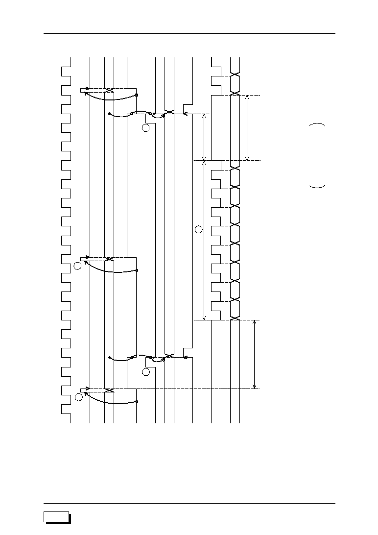
14-18
ML63187/189B/193 User's Manual
Chapter 14 Serial Port (SIO)
M193
TBCCLK
*WSTBUFH
STBUFL/H
BFULL
LSTSF
Send register
STINT
TXD
Interrupt request
generation
TBCCLK
2.5 clocks
A
B
D
E
TBCCLK 3.5 clocks min.
8
1
2
3
4
5
6
7
TXCI
TBCCLK
WSTBUFH
LSTSF
BFULL
STINT
TXCI
TXD
:
:
:
:
:
:
:
Base clock
STBUFH write signal
(*asynchronous to Low-speed clock (32.768 kHz) when system clock is High-speed clock.)
Send start signal
Send buffer status flag
Send interrupt request signal
Shift clock output from PC.1/TXC pin
Send data
PARITY
TBCCLK 3.5 clocks
1
2
for data length 8 bits,
with parity bit
C
Figure 14-7 Send Timing Chart for Synchronous External Clock Mode

14-19
ML63187/189B/193 User's Manual
Chapter 14 Serial Port (SIO)
14
M193
14.4.3 Receive Operation Description
(1) UART mode
The UART mode is specified by setting SRMOD (bit 0 of SRCON0) to "0". Figure
14-8 is the UART mode receive timing chart. The UART mode receive procedure
is described below.
First set the receive baud rate in the receive baud rate setting register (SRBRT).
Supported baud rates for UART mode receive are 1200, 2400, 4800, and 9600
bps.
Set the receive format (data bit length, parity bit, etc.) in SRCON0 and SRCON1.
Set SREN (bit 3 of SRCON0) to "1" to enable receive.
At the negative edge of the receive data (RXD) start bit, receive operation will
start.
Receive operation ends.
If a framing or overrun error occurs the FERR or OERR flag of the status register
(SSTAT) will be set to "1".
Received data is transferred to SRBUFL/H.
If a parity error occurs, the PERR flag of the status register (SSTAT) is set to "1".
The serial port receive interrupt request (SRINT) is generated.
Receive data is received until receive is disabled (SREN = "0"). When receive
is ended, reset the receive enable/disable flag (SREN) to "0".
The receive data sampling clock (SRSMPL) is based on the low-speed clock
supply, not on the high-speed clock. This allows receive operations to be
executed while in the energy-saving mode.
A
C
B
D
E
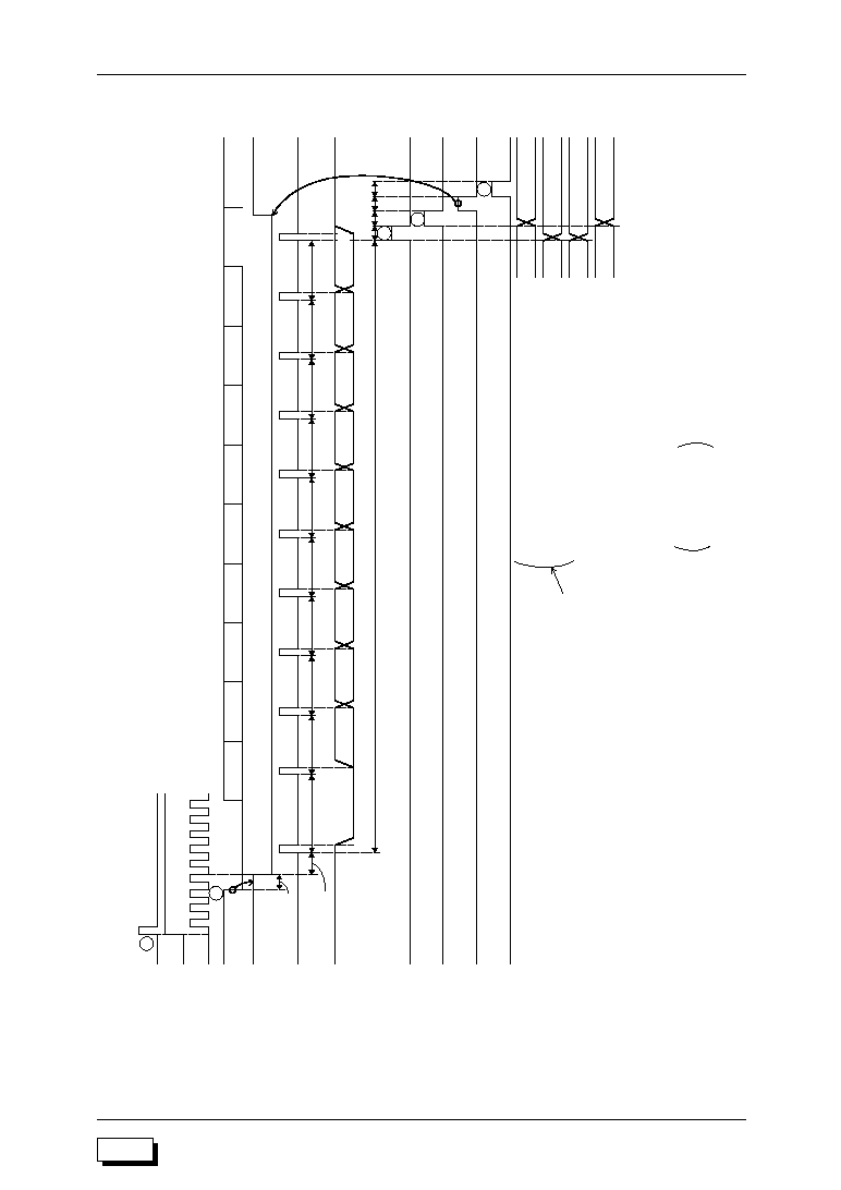
14-20
ML63187/189B/193 User's Manual
Chapter 14 Serial Port (SIO)
M193
Figure 14-8 UART Mode Receive Timing Chart
WSRCONL
SREN
BRTC
RXD
SRFREE
SRSMPL
Receive
shift register
initial state
SREND
LSRBUF
SRINIT
SRINT
A
B
C
D
E
Interrupt
request
generated
Receive data
SRBUFL/H
FERR
OERR
PERR
At least one
clock, less
than 2 clocks
BRTC
1.5 clocks
START BIT
1
2
3
4
5
6
7
8
PARITY BIT
STOP BIT
Ta
Tb
Ta
Ta
Ta
Ta
Tb
Ta
Ta
Ta
START BIT
1
2
3
4
5
6
7
8
STOP BIT
68 BRTC clocks
Tc Tc Tc Tc
Note)
Ta : BRTC 7 clocks
Tb : BRTC 6 clocks
Tc : BRTC 1 clock
WSRCONL
SREN
BRTC
RXD
SRFREE
SRSMPL
SREND
LSRBUF
SRINIT
SRINT
FERR
OERR
PERR
:
:
:
:
:
:
:
:
:
:
:
:
:
SRCONL write signal
Receive enable/disable flag
Base clock for selected baud rate
Receive data input to PC.0/RXD pin
Signal indicating receive in progress (0)
Clock pulse sampling receive data
Receive end signal
Signal to write receive data to SRBUFL/H
Receive circuit initialize signal
Receive interrupt request signal
Framing error flag
Overrun error flag
Parity error flag
Baud rate (BRTC frequency)
∑ 9600 bps ∑ ∑ ∑ 2 TBCCLK
∑ 4800 bps ∑ ∑ ∑ TBCCLK
∑ 2400 bps ∑ ∑ ∑ 1/2 TBCCLK
∑ 1200 bps ∑ ∑ ∑ 1/4 TBCCLK
for data length 8 bits,
with parity bit
PARITY BIT
14-21
ML63187/189B/193 User's Manual
Chapter 14 Serial Port (SIO)
14
M193
(2) Synchronous internal clock mode
The synchronous internal clock mode is selected by setting SRMOD (bit 0 of
SRCON0) to "1" and SRCLK (bit 0 of SRCON1) to "1".
Figure 14-9 is the receive timing chart for the synchronous internal clock mode.
The synchronous internal clock receive procedure is indicated below.
First set the receive format (data bit length, parity bit, etc.) in SRCON1 and
SRCON0.
Set SREN (bit 3 of SRCON0) to "1" (receive enable).
After 3 to 4 BRTC clock cycles later the receive shift clock (RXCO) is generated,
and the receive operation starts.
(The shift clock is supplied from the PC.2/RXC pin.)
At the positive edge of RXCO the data received from the PC.0/RXD pin is written
to the receive register.
Receive operation ends.
If an overrun error occurs the OERR flag in status register (SSTAT) is set to "1".
Received data is transferred to SRBUFL/H.
If a parity error occurs, the PERR flag of status register (SSTAT) is set to "1".
The serial port receive interrupt request signal (SRINT) is generated.
At the negative edge of SRINT, SREN is reset to "0".
Repeat step
A
the required number of times. In the synchronous internal clock
mode the receive baud rate is fixed to TBCCLK.
A
C
D
E
F
B
G
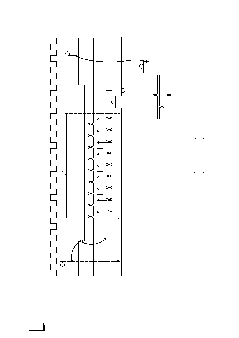
14-22
ML63187/189B/193 User's Manual
Chapter 14 Serial Port (SIO)
M193
G
F
E
D
C
1
2
3
4
5
6
7
8
PARITY
PARITY
1
2
3
4
5
6
7
8
3≠4 BRTC clocks
TBCCLK
WSRCONL
SREN
SRFREE
RXD
RXCO
Receive
shift register
initial state
SREND
LSRBUF
SRINIT
SRINT
SRBUFL/H
OERR
PERR
OERR : Overrun error flag
PERR : Parity error flag
Receive data
TBCCLK
WSRCONL
SREN
SRFREE
RXCO
SREND
LSRBUF
SRINIT
SRINT
RXD
:
:
:
:
:
:
:
:
:
:
Base clock
SRCONL write signal
Receive enable/disable flag
Signal indicating receive in progress (0)
Shift clock output from PC.2/RXC pin
Receive end signal
Signal to write receive data to SRBUFL/H
Receive circuit initialize signal
Receive interrupt request signal
Receive data input to PC.0/RXD pin
for data length 8 bits,
with parity bit
A
B
Figure 14-9 Synchronous Internal Clock Mode Receive Timing Chart

14-23
ML63187/189B/193 User's Manual
Chapter 14 Serial Port (SIO)
14
M193
(3) Synchronous external clock mode
The synchronous external clock mode is selected by setting SRMOD (bit 0 of
SRCON0) to "1" and SRCLK (bit 0 of SRCON1) to "0".
Figure 14-10 is the receive timing chart for the synchronous external clock mode.
The synchronous external clock receive procedure is indicated below.
First set the receive format (data bit length, parity bit, etc.) in SRCON1 and
SRCON0.
Set SREN (bit 3 of SRCON0) to "1" (receive enable).
At the positive edge of the receive shift clock input through PC.2/RXC pin, the
receive data from PC.0/RXD pin is written to the receive register.
Receive operation ends.
If an overrun error occurs the OERR flag in status register (SSTAT) is set to "1".
Received data is transferred to SRBUFL/H.
If a parity error occurs, the PERR flag of status register (SSTAT) is set to "1".
The serial port receive interrupt request signal (SRINT) is generated.
At the negative edge of SRINT, SREN is reset to "0".
Repeat step the required number of times.
In the synchronous external clock mode the receive baud rate is determined by
the external clock (RXCI). Allow at least five clocks (approx. 153
µ
s) of TBCCLK
between the time the receive is enabled (SREN = "1") and the time the external
clock (RXCI) is input.
A
B
C
D
E
A
F
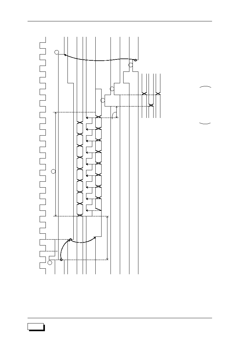
14-24
ML63187/189B/193 User's Manual
Chapter 14 Serial Port (SIO)
M193
Figure 14-10 Synchronous External Clock Mode Receive Timing Chart
F
E
D
C
B
1
2
3
4
5
6
7
8
PARITY
PARITY
1
2
3
4
5
6
7
8
TBCCLK 5 clocks min.
TBCCLK
WSRCONL
SREN
SRFREE
RXD
RXCI
Receive
shift register
initial state
SREND
LSRBUF
SRINIT
SRINT
SRBUFL/H
OERR
PERR
OERR : Overrun error flag
PERR : Parity error flag
Receive data
TBCCLK
WSRCONL
SREN
SRFREE
RXCI
SREND
LSRBUF
SRINIT
SRINT
RXD
:
:
:
:
:
:
:
:
:
:
Base clock
SRCONL write signal
Receive enable/disable flag
Signal indicating receive in progress (0)
Shift clock output from PC.2/RXC pin
Receive end pin
Signal to write receive data to SRBUFL/H
Receive circuit initialize signal
Receive interrupt request signal
Receive data input to PC.0/RXD pin
for data length 8 bits,
with parity bit
Interrupt request
generated
TBCCLK
less than 1 clock
A

14-25
ML63187/189B/193 User's Manual
Chapter 14 Serial Port (SIO)
14
M193
14.5 Send/Receive Data LSB/MSB First Select
Either LSB first or MSB first for send can be selected by setting STLMB (bit 3 of STCON1).
Either LSB first or MSB first for receive can be selected by setting SRLMB (bit 3 of SRCON1).
14.5.1 Selecting Send Data LSB/MSB First
Set STLMB (bit 3 of STCON1) to "0" to select LSB first for send.
The correspondence between LSB first send data and the send buffer register bit is shown
in Figure 14-11. In this case, the LSB is TB0 (bit 0 of STBUFL)
Set STLMB to "1" to send the MSB first.
The correspondence between MSB first send data and the send buffer register bit is shown
in Figure 14-12. In this case, the MSB is TB7 (bit 3 of STBUFH).
TB7
TB6
TB5
TB4
TB3
TB2
TB1
TB0
8
7
6
5
4
3
2
1
TB6
TB5
TB4
TB3
TB2
TB1
TB0
7
6
5
4
3
2
1
TB5
TB4
TB3
TB2
TB1
TB0
6
5
4
3
2
1
TB4
TB3
TB2
TB1
TB0
5
4
3
2
1
(Send first)
Send direction
8 bits
7 bits
6 bits
5 bits
[Send data length]
TB0
TB1
TB2
TB3
TB4
TB5
TB6
TB7
8
7
6
5
4
3
2
1
TB1
TB2
TB3
TB4
TB5
TB6
TB7
7
6
5
4
3
2
1
TB2
TB3
TB4
TB5
TB6
TB7
6
5
4
3
2
1
TB3
TB4
TB5
TB6
TB7
5
4
3
2
1
(Send first)
Send direction
[Send data length]
8 bits
7 bits
6 bits
5 bits
Figure 14-11 Correspondence Between LSB First Send Data and Send Buffer Register
Figure 14-12 Correspondence Between MSB First Send Data and Send Buffer Register
14-26
ML63187/189B/193 User's Manual
Chapter 14 Serial Port (SIO)
M193
RB0
RB1
RB2
RB3
RB4
RB5
RB6
RB7
1
2
3
4
5
6
7
8
RB0
RB1
RB2
RB3
RB4
RB5
RB6
1
2
3
4
5
6
7
(Receive first)
Receive direction
RB0
RB1
RB2
RB3
RB4
RB5
1
2
3
4
5
6
RB0
RB1
RB2
RB3
RB4
1
2
3
4
5
8 bits
7 bits
6 bits
5 bits
[Receive data length]
RB7
RB6
RB5
RB4
RB3
RB2
RB1
RB0
1
2
3
4
5
6
7
8
RB7
RB6
RB5
RB4
RB3
RB2
RB1
1
2
3
4
5
6
7
(Receive first)
Receive direction
RB7
RB6
RB5
RB4
RB3
RB2
1
2
3
4
5
6
RB7
RB6
RB5
RB4
RB3
1
2
3
4
5
[Receive data length]
RB7 not fixed
in this case
RB6, RB7 not fixed
in this case
RB5, RB6, RB7 not fixed
in this case
RB0 not fixed
in this case
RB0, RB1 not fixed
in this case
RB0, RB1, RB2 not fixed
in this case
8 bits
7 bits
6 bits
5 bits
Figure 14-13 Correspondence Between LSB First Receive Data and Receive Buffer Register
Figure 14-14 Correspondence Between MSB First Receive Data and Receive Buffer Register
14.5.2 Selecting Receive Data LSB/MSB First
When the LSB is first in receive data, set SRLMB (bit 3 of SRCON1) to "0".
If the MSB is first, set SRLMB to "1".
The correspondence between receive data and SRBUFL/H bits for LSB first receive is shown
in Figure 14-13, and for MSB first receive in Figure 14-14.

M189B
M187
M193
Chapter 15
15
Shift Register (SFT)


15-1
ML63187/189B/193 User's Manual
Chapter 15 Shift Register (SFT)
M187
M189B
M193
15
Chapter 15 Shift Register (SFT)
15.1 Overview
The ML63187, ML63189B, and ML63193 have one internal 8-bit shift register channel for
clock synchronous communication.
The shift register is synchronized with the clock specified by the shift register control register
0 (SFTCON0), and can perform 8-bit data send and receive simultaneously. When 8-bit data
transfer is completed, a shift register interrupt request is generated.
15.2 Shift Register Configuration
The shift register configuration is shown in Figure 15-1.
PE.0/SIN, PE1/SOUT, and PE.2/SCLK are the shift data input pin, the shift data output pin
and the shift clock input /output pin respectively. Set the secondary function by using port
mode register.
D
Q
CK
R
Transfer complete
Control circuit
SELECT
CK
SO
SI
PE.1/SOUT
PE.2/SCLK
(Master)
ENTR FLAG
SFTINT
PE.2/SCLK
(Slave)
CLK
System reset
PE.0/SIN
Internal bus
MSB/LSB
1/2 CLK
TM1OVF
Figure 15-1 Shift Register Configuration

15-2
ML63187/189B/193 User's Manual
Chapter 15 Shift Register (SFT)
M187
M189B
M193
15.3 Shift Registers
(1) Shift registers L/H (SFTRL, SFTRH)
SFTRL and SFTRH are 4-bit special function registers (SFRs) used to write shift register send
data and to read receive data.
SD3
SD2
SD1
SD0
SFTRL (0A0H)
(R/W)
bit 3
bit 2
bit 1
bit 0
SD7
SD6
SD5
SD4
SFTRH (0A1H)
(R/W)
bit 3
bit 2
bit 1
bit 0
SFTRL and SFTRH are set to "0" at system reset.
15-3
ML63187/189B/193 User's Manual
Chapter 15 Shift Register (SFT)
M187
M189B
M193
15
(2) Shift register control registers (SFTCON0, SFTCON1)
SFTCON0 and SFTCON1 are 4-bit special function registers (SFRs) that control shift register
operation. At system reset both are initialized to "0".
--
SDIR
SELCK1
SELCK0
LSB/MSB first select
1 : MSB first (initial value)
0 : LSB first
SFTCON0 (0A2H)
(R/W)
bit 3
bit 2
bit 1
bit 0
Shift clock select
bit 1 bit 0
0 0 : CLK (initial value)
0 1 : 1/2 CLK
1 0 : Timer 1 overflow
1 1 : External clock
bit 2: SDIR
This bit selects the transfer order for 8-bit send/receive data.
When the SDIR bit is "0" it means MSB first, and when "1", LSB first.
bit 1, 0: SELCK1, SELCK0
These bits select the shift clock.
If set to CLK, 1/2 CLK or timer 1 overflow the system operates in master mode.
If set to external clock the system operates in slave mode.
--
--
--
ENTR
SFTCON1 (0A3H)
(R/W)
bit 3
bit 2
bit 1
bit 0
Transfer start flag
0 : Transfer end (initial value)
1 : Transfer start
bit 0: ENTR
When ENTR is set to "1", transfer starts, and when 8-bit transfer ends, it is
automatically set to "0".
15-4
ML63187/189B/193 User's Manual
Chapter 15 Shift Register (SFT)
M187
M189B
M193
15.4 Shift Register Operation
The shift register can be set to master or slave mode, and to MSB first or LSB first. The send
data is written to the shift register (SFTRL, SFTRH), and transfer is started by setting bit 0
(ENTR) of the shift control register 1 (SFTCON1) to "1". After 8-bit data transfer (send/
receive), operation ends.
Bits 1, 0 (SELCK1, SELCK0) of the shift control register 0 (SFTCON0) can set the shift clock
to CLK, 1/2 CLK or timer 1 overflow. This operation is master mode and the shift clock is
output to the PE.2/SCLK pin.
When the shift clock is set to external clock, the system operates in slave mode, and operation
is to the clock input through the PE.2/SCLK pin. If eight or more clocks are input consecutively,
the ninth and following clocks are ignored.
In both master and slave modes, the shift register is synchronized to the shift clock falling
edge, and shift-out data is output from the first bit through the PE.1/SOUT pin. In synchroni-
zation with the shift clock rising edge, shift-in data is input from the first bit through the PE.0/
SIN pin.
For external devices, shift-in data changes on the falling edge of the shift clock, and shift-out
data changes on the rising edge of the shift clock.
When 8-bit data transfer is complete, bit 0 (ENTR) of SFTCON1 is cleared to "0". When
transfer is completed, the interrupt request signal (SFTINT) is generated (see Figure 15-2).
The output pin state at system reset and between transfers (from the end of one 8-bit transfer
until the next transfer starts) is shown in Table 15-1 (when set to the output secondary
function).
Table 15-1 Output Pin States
Pin name
At system reset
Between transfers
PE.2/SCLK
"H"
"H"
PE.1/SOUT
"L"
Last transfer data of transfer
MSB/LSB first is set to bit 2 (SDIR) of SFTCON0.
Output
Input
SFTRH
SFTRL
∑ SDIR = 1 : LSB first mode
SD7
SD6
SD5
SD4
SD3
SD2
SD1
SD0
Output
Input
SFTRL
SFTRH
∑ SDIR = 0 : MSB first mode
SD0
SD1
SD2
SD3
SD4
SD5
SD6
SD7
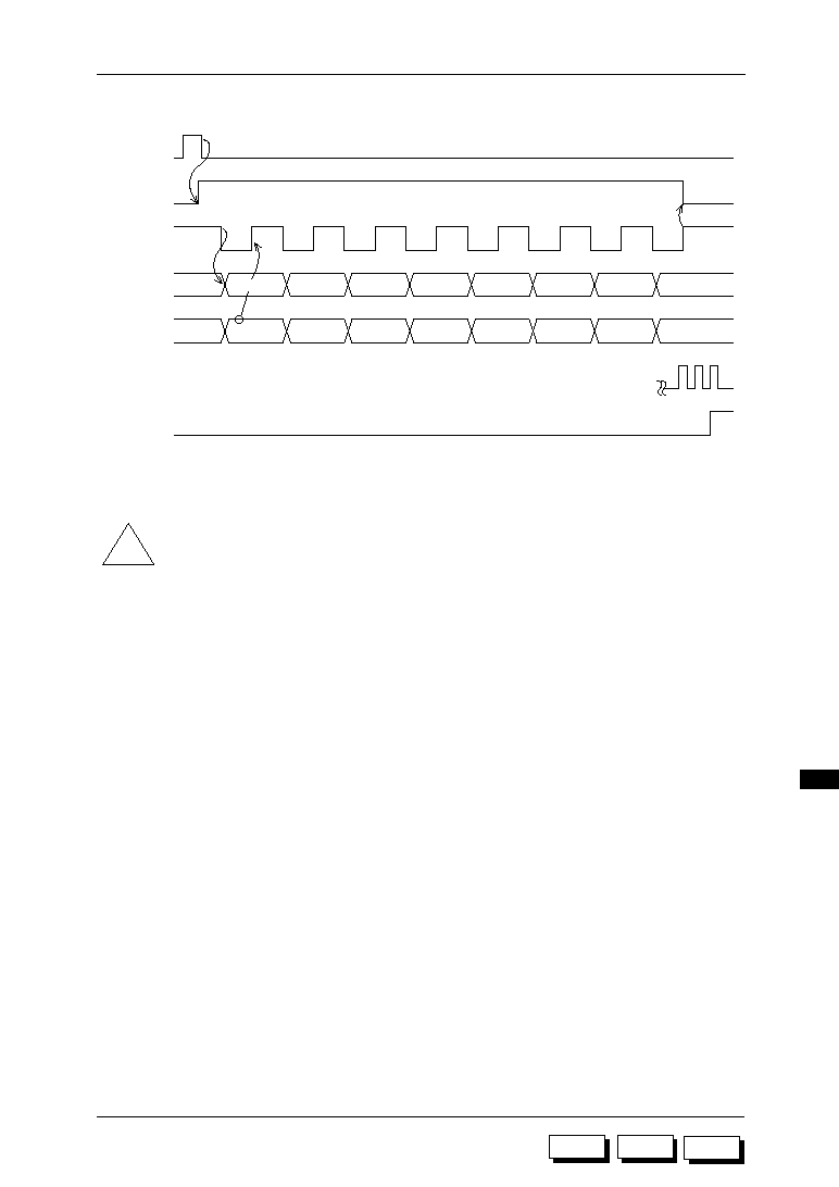
15-5
ML63187/189B/193 User's Manual
Chapter 15 Shift Register (SFT)
M187
M189B
M193
15
DO7
DO6
DO5
DO4
DO3
DO2
DO1
DO0
DI7
DI6
DI5
DI4
DI3
DI2
DI1
DI0
SFTCON1
Write signal
ENTR
SCLK
(PE.2)
SOUT
(PE.1)
SIN
(PE.0)
System clock
SFTINT
Figure 15-2 Shift Register Operation Timing
!
Note :
Setting the ENTR bit to "1" in the slave mode should be done when the PE.2/SCLK pin is high.
If SFTRL/SFTRH are written during transfer, the transfer data (send and receive) is
destroyed. In this case, terminate the transfer and start over again.
Even when receiving only, transfer begins with setting the ENTR bit to "1".
15-6
ML63187/189B/193 User's Manual
Chapter 15 Shift Register (SFT)
M187
M189B
M193
15.5 Shift Register Application Example
An example of register setting for clock synchronous communication using shift register is
described below.
(1) Set the supported port modes (secondary function).
Port control
register
Master mode
Bit 2 = "1"
Bit 1 = "1"
PEMOD
(PE.2/SCLK)
(PE.1/SOUT)
Bit 0 = "1"
(PE.0/SIN)
(2) Select the shift clock with SELCK1, SELCK0 (SFTCON0 bits 1, 0)(master/slave mode
select).
(3) Select MSB first/LSB first with SDIR (SFTCON0 bit 2). ("0" for MSB first, "1" for LSB first).
(4) Set ESFT (IE3 bit 2) to "1" and enable the shift register interrupt.
(5) Set the MIE (master interrupt enable flag) to "1", and enable all interrupts.
(6) Write send data to SFTRL and SFTRH.
(7) Set ENTR (bit 0 of SFTCON1) to "1", and start the transfer.
With the above settings the shift register begins to operate, and the CPU receives the shift
register interrupt. Whether 8-bit transfer has been completed can be checked by monitoring
QSFT (bit 2 of IRQ3) or ENTR (bit 0 of SFTCON1).

M189B
M187
M193
Chapter 16
16
LCD Driver (LCD)

16-1
ML63187/189B/193 User's Manual
Chapter 16 LCD Driver (LCD)
16
M187
M189B
M193
Chapter 16 LCD Driver (LCD)
16.1 Overview
The ML63187, ML63189B, and ML63193 have an internal dot matrix LCD driver. They also
have 64 segment outputs and can drive up to 1024 (64 seg.
•
16 com.) dots. The LCD driver
can be software-selected to all OFF, all ON or power down mode, 1/4 or 1/5 bias, selectable
duty from 1/1 to 1/16, and adjustable (16-tone) contrast.
16.2 LCD Driver Configuration
The LCD driver configuration is shown in Figure 16-1.
Data bus
BIAS
generator
LCD
controller
Display register
(64
• 4 nibbles)
Common driver
Segment driver
COM1
COM16
SEG0
SEG63
Figure 16-1 LCD Driver Configuration

16-2
ML63187/189B/193 User's Manual
Chapter 16 LCD Driver (LCD)
M187
M189B
M193
16.3 LCD Driver Registers
(1) Display control register 0 (DSPCON0)
DSPCON0 is a 4-bit special function register (SFR) controlling LCD driver operation.
bit 3: BISEL
This bit selects 1/4 or 1/5 bias.
At system reset it is "0", selecting 1/5 bias.
bit 2: PDWN
This bit selects the LCD power down mode. When PDWN is set to "1", the bias
generation circuit stops its voltage lowering/raising operation and pins COM1≠16
and SEG0≠63 are all set to the V
SS
level, reducing supply current. At system reset
it is cleared to "0".
bit 1: ALLON
When ALLON is set to "1" all segment drivers are turned on. The ALLON bit has
priority over the LCDON bit. At system reset it is cleared to "0".
bit 0: LCDON
When the LCDON bit is set to "1", the display data in the display register is output
to the segment drivers. At system reset it is cleared to "0", and all segment drivers
are turned off.
BISEL
PDWN
ALLON
LCDON
LCD bias select
0 : 1/5 bias (initial value)
1 : 1/4 bias
LCD power down mode
0 : Normal operation mode (initial value)
1 : Power down mode
All-ON mode
0 : Normal operation mode (initial value)
1 : All-ON mode
LCD display select
0 : All OFF (initial value)
1 : Normal operation mode
DSPCON0 (090H)
(R/W)
bit 3
bit 2
bit 1
bit 0

16-3
ML63187/189B/193 User's Manual
Chapter 16 LCD Driver (LCD)
16
M187
M189B
M193
CN3
CN2
CN1
CN0
DSPCNT (092H)
(R/W)
Contrast select
bit 3 bit 2 bit 1 bit 0
0 0 0 0 : Light (initial value)
0 0 0 1 :
0 0 1 0 :
0 0 1 1 :
0 1 0 0 :
0 1 0 1 :
0 1 1 0 :
0 1 1 1 :
1 0 0 0 :
1 0 0 1 :
1 0 1 0 :
1 0 1 1 :
1 1 0 0 :
1 1 0 1 :
1 1 1 0 :
1 1 1 1 : Dark
bit 3
bit 2
bit 1
bit 0
DT3
DT2
DT1
DT0
DSPCON1 (091H)
(R/W)
Duty select
bit 3 bit 2 bit 1 bit 0
0 0 0 0 : 1/16 duty (initial value)
0 0 0 1 : 1/1 duty
0 0 1 0 : 1/2 duty
0 0 1 1 : 1/3 duty
0 1 0 0 : 1/4 duty
0 1 0 1 : 1/5 duty
0 1 1 0 : 1/6 duty
0 1 1 1 : 1/7 duty
1 0 0 0 : 1/8 duty
1 0 0 1 : 1/9 duty
1 0 1 0 : 1/10 duty
1 0 1 1 : 1/11 duty
1 1 0 0 : 1/12 duty
1 1 0 1 : 1/13 duty
1 1 1 0 : 1/14 duty
1 1 1 1 : 1/15 duty
bit 3
bit 2
bit 1
bit 0
(2) Display control register 1 (DSPCON1)
DSPCON1 is a 4-bit special function register (SFR) used to select the LCD driver duty.
At system reset, bits of DSPCON1 are initialized to "0".
(3) Display contrast register (DSPCNT)
DSPCNT is a 4-bit special function register (SFR) used to adjust display contrast.
At system reset, bits of DSPCON1 are initialized to "0".
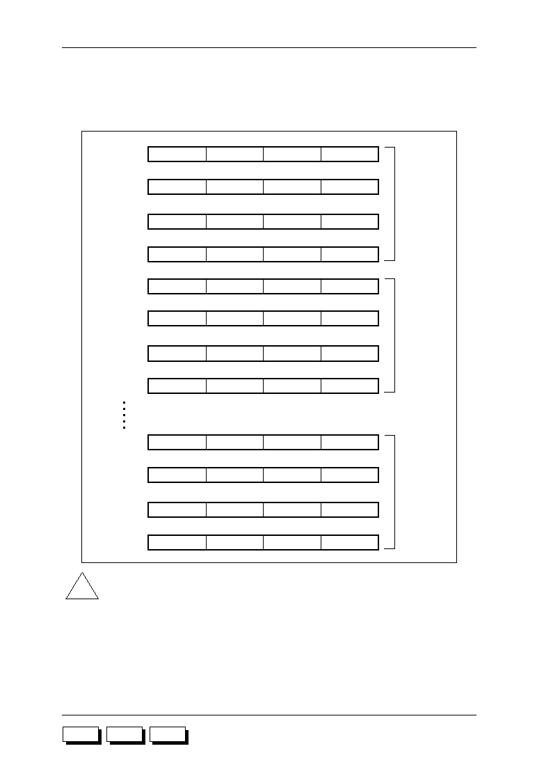
16-4
ML63187/189B/193 User's Manual
Chapter 16 LCD Driver (LCD)
M187
M189B
M193
(4) Display registers (DSPR0 to DSPR255)
DSPR0 to DSPR255 are segment output data registers for the dot matrix LCD driver allocated
to RAM BANK 1. The correspondence between display registers and segment outputs is
shown below.
!
Notes:
∑ When a display register bit is set to "1", the corresponding LCD dot lights. When reset to
"0" it goes off.
∑ To keep stable display state, each individual LCD dot should be set to ON/OFF with bit
operation instructions.
∑ At system reset the display registers (DSPR0 to DSPR255) are undefined and should be
initialized.
COM4
COM3
COM2
COM1
DSPR4 (104H)
(R/W)
bit 3
bit 2
bit 1
bit 0
COM8
COM7
COM6
COM5
DSPR5 (105H)
(R/W)
bit 3
bit 2
bit 1
bit 0
COM12
COM11
COM10
COM9
DSPR6 (106H)
(R/W)
bit 3
bit 2
bit 1
bit 0
COM16
COM15
COM14
COM13
DSPR7 (107H)
(R/W)
bit 3
bit 2
bit 1
bit 0
Segment 1
output data
COM4
COM3
COM2
COM1
DSPR252 (1FCH)
(R/W)
bit 3
bit 2
bit 1
bit 0
COM8
COM7
COM6
COM5
DSPR253 (1FDH)
(R/W)
bit 3
bit 2
bit 1
bit 0
COM12
COM11
COM10
COM9
DSPR254 (1FEH)
(R/W)
bit 3
bit 2
bit 1
bit 0
COM16
COM15
COM14
COM13
DSPR255 (1FFH)
(R/W)
bit 3
bit 2
bit 1
bit 0
Segment 63
output data
COM4
COM3
COM2
COM1
DSPR0 (100H)
(R/W)
bit 3
bit 2
bit 1
bit 0
COM8
COM7
COM6
COM5
DSPR1 (101H)
(R/W)
bit 3
bit 2
bit 1
bit 0
COM12
COM11
COM10
COM9
DSPR2 (102H)
(R/W)
bit 3
bit 2
bit 1
bit 0
COM16
COM15
COM14
COM13
DSPR3 (103H)
(R/W)
bit 3
bit 2
bit 1
bit 0
Segment 0
output data

16-5
ML63187/189B/193 User's Manual
Chapter 16 LCD Driver (LCD)
16
M187
M189B
M193
16.4 LCD Driver Operation
The display duty is selected from 1/1 to 1/16 using DSPCON. The frame frequency for each
duty ratio is indicated in Table 16-1. Depending on the duty selected, the common signal
(COM1 to COM16) is generated, and data written in synchronization with that common signal
to the display registers (DSPR0 to DSPR255) is output to the segment driver. The segment
driver uses bits 0, 1 (ALLON, LCDON) of the display control register 0 (DSPCON0) to control
all OFF or all ON modes.
When PDWN (bit 2 of DSPCON0) is set to "1", the LCD power down mode is enabled. In the
LCD power-down mode the bias generation circuit operation stops, and COM1≠16 and
SEG0≠63 pins are all output at the V
SS
level to reduce supply current.
BISEL (bit3 of DSPCON0) selects 1/4 or 1/5 bias.
DSPCNT controls the LCD contrast of 16 tones (V
DDH
= 2.4 V or more).
When the LCD driver is not used, select the power-down mode and set all the bits of the
display control register (DSPCNT) to "0" to save the supply current.
Table 16-1 Frame Frequency for Each Duty
DSPCON1
DT3 DT2 DT1 DT0
Duty
Frame
frequency
0
0
0
0
1/16
64 Hz
0
0
0
1
1/1
1024 Hz
0
0
1
0
1/2
512 Hz
0
0
1
1
1/3
approx. 341 Hz
0
1
0
0
1/4
256 Hz
0
1
0
1
1/5
approx. 205 Hz
0
1
1
0
1/6
approx. 171 Hz
0
1
1
1
1/7
approx. 146 Hz
1
0
0
0
1/8
128 Hz
1
0
0
1
1/9
approx. 114 Hz
1
0
1
0
1/10
approx. 102 Hz
1
0
1
1
1/11
approx. 93 Hz
1
1
0
0
1/12
approx. 85 Hz
1
1
0
1
1/13
approx. 79 Hz
1
1
1
0
1/14
approx. 73 Hz
1
1
1
1
1/15
approx. 68 Hz
DT3≠0
0H
1H
2H
3H
4H
5H
6H
7H
8H
9H
0AH
0BH
0CH
0DH
0EH
0FH

16-6
ML63187/189B/193 User's Manual
Chapter 16 LCD Driver (LCD)
M187
M189B
M193
Figure 16-2 Bias Generator Configuration for 1/5 Bias
16.5 Bias Generator (BIAS)
The bias generator is used to multiply and divide the voltage (V
DD2
) generated in the constant
voltage circuit with an external capacitor connected to pins C1, C2 to generate V
DD1
to V
DD5
bias voltages for the LCD driver.
The LCD power down mode stops the voltage lowering/raising operation of the bias
generation circuit in order to reduce supply current.
Figure 16-2 shows the bias generator configuration for 1/5 bias, and Figure 16-3 shows the
configuration for 1/4 bias. For details of the backup circuit and the constant-voltage circuit,
see Chapter 19, "Backup Circuit."
Tables 16-2 and 16-3 show the table of display contrast adjusting voltages.
Backup
circuit
Display contrast adjustment
(CN3≠0)
1/5 bias select
(BISEL = "0")
To LCD driver
Constant voltage
circuit
BIAS
generator
V
DDH
V
DDH
V
DD
CB1
CB2
V
DD5
V
DD4
V
DD3
V
DD2
V
DD1
V
SS
C1
V
SS
C2
C
12
C
a
C
b
C
c
C
d
C
e
C
b12
C
h
Power down mode select
(PDWN = "1")
V
DDL
C
l

16-7
ML63187/189B/193 User's Manual
Chapter 16 LCD Driver (LCD)
16
M187
M189B
M193
Figure 16-3 Bias Generator Configuration for 1/4 Bias
Backup
circuit
Display contrast adjustment
(CN3≠0)
1/4 bias select
(BISEL = "1")
To LCD driver
Constant voltage
circuit
BIAS
generator
V
DDH
V
DDH
V
DD
CB1
CB2
V
DD5
V
DD4
V
DD3
V
DD2
V
DD1
V
SS
C1
V
SS
C2
C
12
C
a
C
b
C
d
C
e
C
b12
C
h
Power down mode select
(PDWN = "1")
V
DDL
C
l
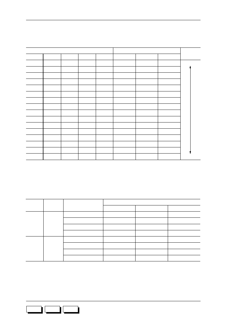
16-8
ML63187/189B/193 User's Manual
Chapter 16 LCD Driver (LCD)
M187
M189B
M193
V
DD2
*: Typical V
DD2
in Table 16-2
Table 16-2 Display Contrast Adjusting Voltages (V
DD2
)
Table 16-3 Display Contrast Adjusting Voltages (V
DD1
, V
DD3
, V
DD4
, V
DD5
)
DSPCNT
V
DD2
Voltage (V)
CN3≠0
CN3
CN2
CN1
CN0
Min.
Typ.
Max.
Contrast
0H
0
0
0
0
1.70
1.80
1.90
1H
0
0
0
1
1.74
1.84
1.94
2H
0
0
1
0
1.78
1.88
1.98
3H
0
0
1
1
1.82
1.92
2.02
4H
0
1
0
0
1.86
1.96
2.06
5H
0
1
0
1
1.90
2.00
2.10
6H
0
1
1
0
1.94
2.04
2.14
7H
0
1
1
1
1.98
2.08
2.18
8H
1
0
0
0
2.02
2.12
2.22
9H
1
0
0
1
2.06
2.16
2.26
0AH
1
0
1
0
2.10
2.20
2.30
0BH
1
0
1
1
2.14
2.24
2.34
0CH
1
1
0
0
2.18
2.28
2.38
0DH
1
1
0
1
2.22
2.32
2.42
0EH
1
1
1
0
2.26
2.36
2.46
0FH
1
1
1
1
2.30
2.40
2.50
Light
Dark
(Ta = 25∞C, V
SS
= 0 V)
BISEL
Mode
Voltage (V)
Power supply
Min.
Typ.
Max.
0
1/5 bias
V
DD1
Typ. ≠ 0.1
1/2
• V
DD2
*
Typ. + 0.1
V
DD3
Typ. ≠ 0.3
3/2
• V
DD2
*
Typ. + 0.3
V
DD4
Typ. ≠ 0.4
2
• V
DD2
*
Typ. + 0.4
V
DD5
Typ. ≠ 0.5
5/2
• V
DD2
*
Typ. + 0.5
V
DD1
Typ. ≠ 0.1
1/2
• V
DD2
*
Typ. + 0.1
V
DD3
Typ. ≠ 0.2
V
DD2
*
Typ. + 0.2
V
DD4
Typ. ≠ 0.3
3/2
• V
DD2
*
Typ. + 0.3
V
DD5
Typ. ≠ 0.4
2
• V
DD2
*
Typ. + 0.4
1
1/4 bias
(V
SS
= 0 V)

16-9
ML63187/189B/193 User's Manual
Chapter 16 LCD Driver (LCD)
16
M187
M189B
M193
16.6 LCD Driver Output Waveform
Figures 16-4 (a) and 16-4 (b) show the output waveforms for 1/16 duty and 1/5 bias, and
Figures 16-5 (a) and 16-5 (b) show the output waveforms for 1/8 duty and 1/4 bias.
Figure 16-4 (a) 1/16 Duty, 1/5 Bias Common Output Waveform
V
SS
V
DD1
V
DD2
V
DD3
V
DD4
V
DD5
1
2
3
4
5
∑ ∑ ∑ ∑
16 1
2
3
4
5
∑ ∑ ∑ ∑
16
V
SS
V
DD1
V
DD2
V
DD3
V
DD4
V
DD5
V
SS
V
DD1
V
DD2
V
DD3
V
DD4
V
DD5
V
SS
V
DD1
V
DD2
V
DD3
V
DD4
V
DD5
Frame frequency 64 Hz
COM1
COM2
COM3
COM16
∑
∑
∑
∑
∑
16-10
ML63187/189B/193 User's Manual
Chapter 16 LCD Driver (LCD)
M187
M189B
M193
1
2
3
4
5
6
7
8
9 10 11 12 13 14 15 16 1
2
3
4
5
6
7
8
9 10 11 12 13 14 15 16
Frame frequency 64 Hz
SEG0
SEG1
SEG2
COM1
COM2
COM3
COM4
COM5
COM6
COM7
COM8
COM9
COM10
COM11
COM12
COM13
COM14
COM15
COM16
SEG0
SEG1
SEG2
SEG3
SEG4
V
DD5
V
DD4
V
DD3
V
DD2
V
DD1
V
SS
V
DD5
V
DD4
V
DD3
V
DD2
V
DD1
V
SS
V
DD5
V
DD4
V
DD3
V
DD2
V
DD1
V
SS
Figure 16-4 (b) 1/16 Duty, 1/5 Bias Segment Output Waveform
16-11
ML63187/189B/193 User's Manual
Chapter 16 LCD Driver (LCD)
16
M187
M189B
M193
V
DD5
V
DD4
V
DD2,3
V
DD1
V
SS
V
DD5
V
DD4
V
DD2,3
V
DD1
V
SS
V
DD5
V
DD4
V
DD2,3
V
DD1
V
SS
COM1
COM2
COM3
∑
∑
∑
∑
∑
∑
1
2
3
4
5
6
7
8
1
2
3
4
5
6
7
8
Frame frequency 128 Hz
V
DD5
V
DD4
V
DD2,3
V
DD1
V
SS
COM8
V
DD5
V
DD4
V
DD2,3
V
DD1
V
SS
COM9≠16
Figure 16-5 (a) 1/8 Duty, 1/4 Bias Common Output Waveform
16-12
ML63187/189B/193 User's Manual
Chapter 16 LCD Driver (LCD)
M187
M189B
M193
V
DD5
V
DD4
V
DD2,3
V
DD1
V
SS
V
DD5
V
DD4
V
DD2,3
V
DD1
V
SS
V
DD5
V
DD4
V
DD2,3
V
DD1
V
SS
SEG0
SEG1
SEG2
1
2
3
4
5
6
7
8
1
2
3
4
5
6
7
8
Frame frequency 128 Hz
COM1
COM2
COM3
COM4
COM5
COM6
COM7
COM8
SEG0
SEG1
SEG2
SEG3
SEG4
Figure 16-5 (b) 1/8 Duty, 1/4 Bias Segment Output Waveform

M189B
M187
M193
Chapter 17
Multiplication/Division Circuit
(MULDIV)
17


17-1
ML63187/189B/193 User's Manual
Chapter 17 Multiplication/Division Circuit (MULDIV)
M187
M189B
M193
17
Chapter 17 Multiplication/Division Circuit (MULDIV)
17.1 Overview
The ML63193 has an 8-bit
◊
8-bit = 16-bit multiplication (MUL) and a 16-bit/8-bit = 16-bit
division (DIV), implemented with an internal circuit.
The registers used are shown in Table 17-1.
Table 17-1 Registers Used in Multiplication and Division Circuit
Register name
Symbol
Address bit 3 bit 2 bit 1 bit 0
R/W
Value at
system reset
Multiplication/division condition register
MDCR
086H
OV
EF
DIVS MULS R/W
0H
C register L
CRL
087H
CR3
CR2
CR1
CR0
R/W
0H
C register H
CRH
088H
CR7
CR6
CR5
CR4
R/W
0H
D register L
DRL
089H
DR3
DR2
DR1
DR0
R/W
0H
D register H
DRH
08AH
DR7
DR6
DR5
DR4
R/W
0H
E register L
ERL
08BH
ER3
ER2
ER1
ER0
R/W
0H
E register H
ERH
08CH
ER7
ER6
ER5
ER4
R/W
0H
F register L
FRL
08DH
FR3
FR2
FR1
FR0
R/W
0H
F register H
FRH
08EH
FR7
FR6
FR5
FR4
R/W
0H
For multiplication the C register is multiplied by the E register. The result is stored in the DC
register (D: high-order 8 bits, C: low-order 8 bits) after 5 machine cycles.
For division the D register is divided by the E register. The result is stored in the DC register
(dividend) and F register (remainder) after 10 machine cycles.

17-2
ML63187/189B/193 User's Manual
Chapter 17 Multiplication/Division Circuit (MULDIV)
M187
M189B
M193
ER3
ER2
ER1
ER0
ERL (08BH)
(R/W)
bit 3
bit 2
bit 1
bit 0
ER7
ER6
ER5
ER4
ERH (08CH)
(R/W)
bit 3
bit 2
bit 1
bit 0
FR3
FR2
FR1
FR0
FRL (08DH)
(R/W)
bit 3
bit 2
bit 1
bit 0
FR7
FR6
FR5
FR4
FRH (08EH)
(R/W)
bit 3
bit 2
bit 1
bit 0
CR3
CR2
CR1
CR0
CRL (087H)
(R/W)
bit 3
bit 2
bit 1
bit 0
CR7
CR6
CR5
CR4
CRH (088H)
(R/W)
bit 3
bit 2
bit 1
bit 0
DR3
DR2
DR1
DR0
DRL (089H)
(R/W)
bit 3
bit 2
bit 1
bit 0
DR7
DR6
DR5
DR4
DRH (08AH)
(R/W)
bit 3
bit 2
bit 1
bit 0
17.2 Multiplication and Division Registers
17.2.1 Calculation Registers
The multiplication and division calculation registers (CRL, CRH, DRL, DRH, ERL, ERH, FRL,
FRH) are 4-bit special function registers (SFRs), used to set multiplier, multiplicand, divisor,
and dividend and store results.
M193

17-3
ML63187/189B/193 User's Manual
Chapter 17 Multiplication/Division Circuit (MULDIV)
M187
M189B
M193
17
The multiplication and division calculation registers are used as follows.
[Multiplication]
DR∑CR
CR
◊
ER
CR (CRH, CRL):
Holds the multiplicand. After multiplication, holds the low-order 8 bits
of the result.
ER (ERH, ERL):
Holds the multiplier. After multiplication, holds data.
DR (DRH, DRL):
After execution, the high-order 8 bits of the result are stored.
If the result of multiplication cannot be stored in the low-order 8 bits (DR is not 0), the
multiplication/division condition register (MDCR) OV flag is set to "1". When bit 0 (MULS) of
MDCR is set to "1", multiplication starts, and the result is output to the appropriate registers
five machine cycles later.
[Division]
DR∑CR
DR∑CR/ER
FR
DR∑CR mod ER
DR (DRH, DRL):
The high-order 8 bits of the number being divided are set here. After
execution, this register holds the high-order 8 bits of the result.
CR (CRH, CRL):
The low-order 8 bits of the number being divided are set here. After
execution, this register holds the low-order 8 bits of the result.
ER (ERH, ERL):
The divisor is set here. After execution, this register holds data.
FR (FRH, FRL):
After execution, this register holds the remainder.
If division is executed with ER = 00H (division by zero), the MDCR EF flag is set to "1". After
division by zero the DC register value is 0FFFFH, and the pre-execution value from the C
register is set to the F register. When bit 1 (DIVS) of MDCR is set to "1", division begins and
the result is output to the appropriate registers ten machine cycles later.
17-4
ML63187/189B/193 User's Manual
Chapter 17 Multiplication/Division Circuit (MULDIV)
M187
M189B
M193
17.2.2 Multiplication/Division Condition Register
The multiplication/division condition register (MDCR) is a 4-bit special function register (SFR)
with a multiplication/division start flag and a status flag indicating the status of the operation
when finished.
OV
EF
DIVS
MULS
MDCR (086H)
(R/W)
bit 3
bit 2
bit 1
bit 0
Overflow flag
0 : (initial value)
1 : When result of 8-bit
• 8-bit multiplication is more than 8 bits (D register 0)
Error flag
0 : (initial value)
1 : Division by zero (E register = 00H)
Division start flag
0 : Stop (initial value)
1 : Start
Multiplication start flag
0 : Stop (initial value)
1 : Start
bit 3: OV (OVerflow flag)
Set to "1" when there is a carry (D register other than 00H) to the high-order 8 bits
in multiplication, and otherwise cleared to "0".
This bit is initialized to "0" at system reset.
bit 2: EF (Error Flag)
Set to "1" when the E register is "0" in division, and otherwise cleared to "0".
This bit is initialized to "0" at system reset.
bit 1: DIVS (DIV Start)
Division is started when this bit is set to "1", and is completes in ten machine
cycles. When division is complete DIVS is reset to "0".
This bit initializes to "0" at system reset.
bit 0: MULS (MUL Start)
This flag starts multiplication when set to "1", and multiplication is completes in five
machine cycles. MULS is cleared to "0" when multiplication is complete.
This bit is reset to "0" at system reset.
M193

17-5
ML63187/189B/193 User's Manual
Chapter 17 Multiplication/Division Circuit (MULDIV)
M187
M189B
M193
17
17.3 Multiplication/Division Execution
Multiplication and division execution is handled as follows.
[Multiplication]
1. Multiplicand set to C register (CRH, CRL)
2. Multiplier set to E register (ERH, ERL)
3. MDCR MULS flag set to "1".
[Division]
1. High-order 8 bits of number being divided set to D register (DRH, DRL), and low-
order 8 bits to C register (CRH, CRL).
2. Divisor set to E register (ERH, ERL).
3. MDCR DIVS flag set to "1".

17-6
ML63187/189B/193 User's Manual
Chapter 17 Multiplication/Division Circuit (MULDIV)
M187
M189B
M193
M193

M189B
M187
M193
Chapter 18
Battery Low Detect Circuit
(BLD)
18


18-1
ML63187/189B/193 User's Manual
Chapter 18 Battery Low Detect Circuit (BLD)
M187
M189B
M193
18
Chapter 18 Battery Low Detect Circuit (BLD)
18.1 Overview
The ML63187, ML63189B, and ML63193 have an internal battery low detect circuit (BLD).
The battery low detect circuit detects when the battery voltage (supply voltage V
DD
) falls
below the judgment voltage value. Four levels of judgment voltage can be selected by the
BLDCON bits.
Judgment voltage values (Ta = 25
∞
C): 1.05
±
0.10 V, 1.20
±
0.10 V, 1.80
±
0.10 V, 2.40
±
0.10 V
!
Note:
∑
When verifying BLD operation, the operation must be verified with an evaluation sample
device.
The OTP (MSM63P180) and development/support tool (EASE63180) do not support
BLD.
(The BLD judgment voltage value of the ML63187, ML63189B, and ML63193 is different
from that of the MSM63182, MSM63184B, MSM63188, MSM63182A, MSM63184A, and
MSM63188A of the same series.)
18.2 Battery Low Detect Circuit Configuration
The battery low detect circuit consists of a judgment circuit and a judgment voltage select
circuit. Figure 18-1 shows the circuit configuration.
Figure 18-1 Battery Low Detect Circuit
V
DD
Judgment circuit
Judgment voltage
select circuit
ENBL
BLDF
Read BLDCON
4
Data bus
BLDCON
3
Q
I/O

18-2
ML63187/189B/193 User's Manual
Chapter 18 Battery Low Detect Circuit (BLD)
M187
M189B
M193
18.3 Judgment Voltage
The value of the judgment voltage is selected by the software by setting the LD1 (bit 1 of
BLDCON) and LD0 (bit 0 of BLDCON) bits.
Table 18-1 lists judgment voltage and precision values.
Table 18-1 Judgment Voltage
LD1
LD0
Judgment voltage (V)
Remarks
0
0
1.05
Ta = 25∞C
0
1
1.20
Ta = 25∞C
1
0
1.80
Ta = 25∞C
1
1
2.40
Ta = 25∞C
Precision (V)
±0.10
±0.10
±0.10
±0.10
18.4 Battery Low Detect Circuit Register
∑
Battery low detect control register (BLDCON)
BLDCON is a 4-bit special function register (SFR) that controls the battery low
detect circuit.
BLDF
ENBL
LD1
LD0
Judgment result flag
0: Higher than judgment value (initial value)
1: Lower than judgment value
BLDCON (094H)
(R/W)
bit 3
bit 2
bit 1
bit 0
Judgment voltage select
bit 1 bit 0
0 0 : 1.05 ±0.10 V (initial value)
0 1 : 1.20 ±0.10 V
1 0 : 1.80 ±0.10 V
1 1 : 2.40 ±0.10 V
Battery low detect circuit ON/OFF control
0: Battery low detect circuit OFF (initial value)
1: Battery low detect circuit ON
bit 3: BLDF
This flag indicates the judgement result of the battery low detect circuit.
This bit is set to "1" when V
DD
is lower than the judgment voltage selected by LD0
and LD1, and is set to "0" when V
DD
is higher. This bit is "0" when the BLD circuit
stops operation.
This bit is read-only and writes are invalid.
bit 2: ENBL
This bit turns the battery low detect circuit ON or OFF.
When ENBL is set to "1", the battery low detect circuit is ON. When ENBL is set
to "0", the battery low detect circuit is OFF.
At system reset, this bit is cleared to "0".
bit 1, 0: LD1, LD0
These bits select the judgment voltage.
At system reset, these bits are cleared to "0".
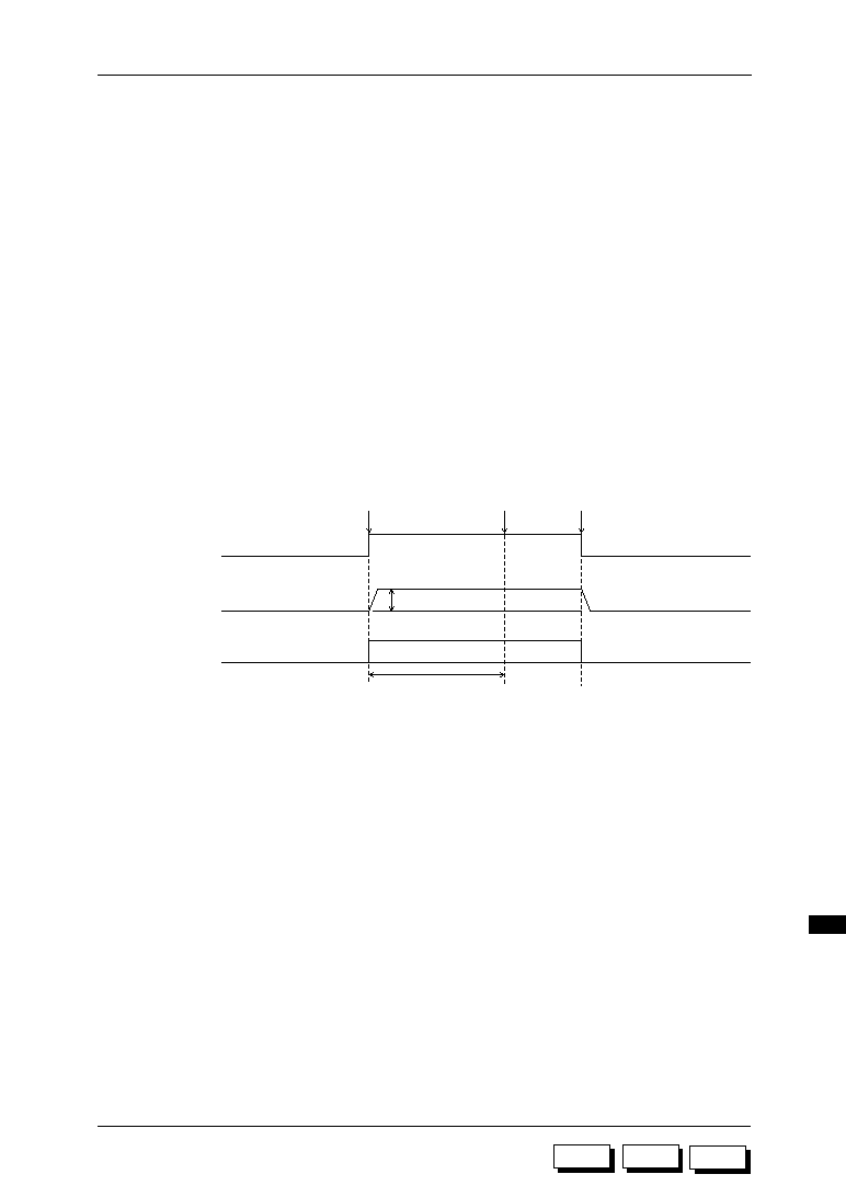
18-3
ML63187/189B/193 User's Manual
Chapter 18 Battery Low Detect Circuit (BLD)
M187
M189B
M193
18
18.5 Battery Low Detect Circuit Operation
The battery low circuit is turned ON or OFF by ENBL (bit 2 of BLDCON), and outputs to BLDF
(bit 3 of BLDCON) the result of a comparison with the judgment voltage.
ENBL is the enable control bit for the battery low detect circuit. Setting ENBL to "1" turns ON
the battery low detect circuit. Setting ENBL to "0" turns OFF the battery low detect circuit and
BLD current supply drops to zero.
BLDF is the judgment result flag. If BLDF is "1", the power supply voltage is lower than the
judgment voltage. If BLDF is "0", the power supply voltage is higher than the judgment
voltage. BLDF is valid when ENBL is "1".
The judgment circuit of the battery low detect circuit requires time to become stable.
Therefore, after setting ENBL to "1", wait at least 1 ms before reading BLDF. No load should
be applied to the power supply voltage during the detection.
Figure 18-2 shows an example operation timing.
Judgment voltage
Vcmp
BLDF
V
SS
"1" or "0"
Vcmp
ENBL
q
w
r
e
Operation
BLD stabilization time
(wait at least 1 ms)
Set ENBL
Read BLDF
Reset ENBL
Figure 18-2 Operation Timing Example
Figure 18-2 shows the following operations.
q
ENBL is set to "1" to turn ON the BLD.
w
Operation starts with no load applied to power supply system and waits for BLD
stabilization time interval (at least 1 ms).
e
Judgment result flag (BLDF) is read.
r
ENBL is cleared to "0".

18-4
ML63187/189B/193 User's Manual
Chapter 18 Battery Low Detect Circuit (BLD)
M187
M189B
M193

M189B
M187
M193
Chapter 19
Backup Circuit (BACKUP)
19


19-1
ML63187/189B/193 User's Manual
Chapter 19 Backup Circuit (BACKUP)
M187
M189B
M193
19
Chapter 19 Backup Circuit (BACKUP)
19.1 Overview
The ML63187, ML63189B, and ML63193 contain a voltage backup circuit that doubles the
power supply voltage. The backup circuit is used when the power supply voltage is 1.8 V or
less.
By operating the backup circuit, the CPU can be run even when the power supply voltage is
0.9 V.
The voltage boosted by the backup circuit is supplied as V
DDH
to the constant voltage circuit
and to the high-speed oscillation circuit.
The constant voltage circuit generates V
DDL
(voltage for internal logic) and V
DD2
(bias
reference voltage for LCDs).
Depending upon whether the backup circuit is ON or OFF, the following voltages are supplied
to V
DDH
(voltage supplied to the constant voltage circuit and high-speed oscillation circuit).
∑
When backup circuit is ON
Voltage that is doubled by the backup circuit
∑
When backup circuit is OFF
Power supply voltage
Power supply specifications are determined depending upon whether the backup circuit is
used.
When backup circuit is used
∑ ∑ ∑ V
DD
= 0.9 to 2.7 V
When backup circuit is not used ∑ ∑ ∑ V
DD
= 1.8 to 5.5 V
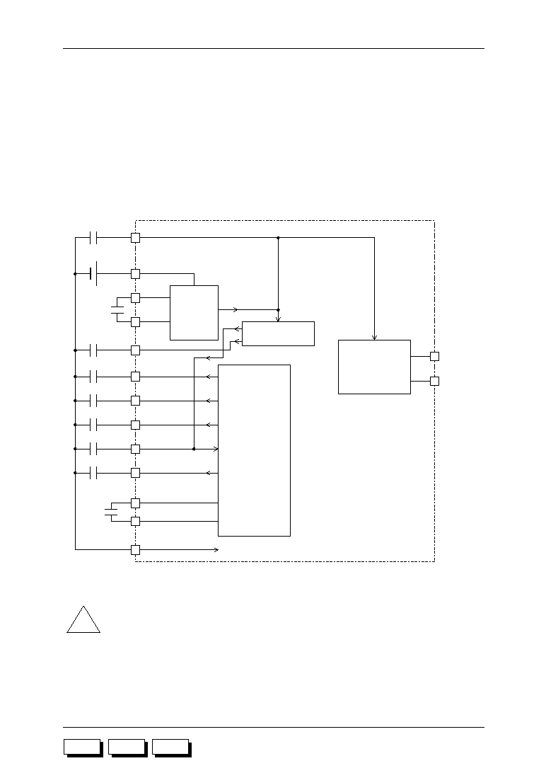
19-2
ML63187/189B/193 User's Manual
Chapter 19 Backup Circuit (BACKUP)
M187
M189B
M193
19.2 Power Supply Circuit Configuration
19.2.1 Power Supply Circuit Configuration When Backup Circuit is Used
Figure 19-1 shows the power supply circuit configuration when the backup circuit is used.
To use the backup circuit, connect a capacitor (C
b12
) between the CB1 and CB2 pins, or
connect a capacitor (C
h
) between V
DDH
and V
SS
.
In addition, at the beginning of the program, set the backup select bit BACKUP (bit 0 of
BUPCON) to "1". The backup select bit is described in a later section.
Figure 19-1 Power Supply Circuit Configuration When Backup Circuit is Used
!
Notes:
∑
In systems that use the backup circuit, connect an external capacitor (C
b12
)
between the CB1 and CB2 pins.
∑
The backup circuit cannot be switched ON/OFF once operation has begun.
Design peripheral circuits such as external capacitor C
b12
to meet the ON/OFF
specification of the backup circuit.
OSC1
OSC0
High-speed
oscillation
circuit
Constant voltage
circuit
Bias generator
V
DDH
V
DD
CB1
CB2
V
DD5
V
DD4
V
DD3
V
DD2
V
DD1
C1
C2
V
SS
C
12
C
a
C
b
C
c
C
d
C
e
C
b12
C
h
0.9 to 2.7 V
Backup
circuit
V
DDL
C
l
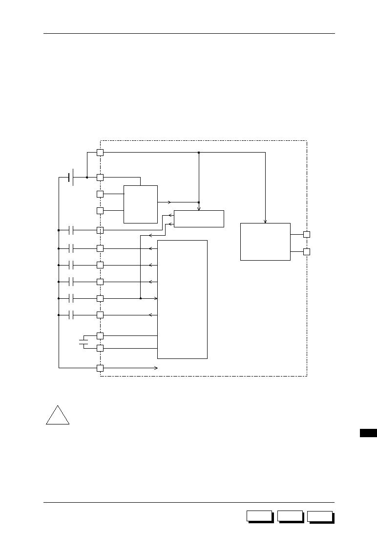
19-3
ML63187/189B/193 User's Manual
Chapter 19 Backup Circuit (BACKUP)
M187
M189B
M193
19
19.2.2 Power Supply Circuit Configuration When Backup Circuit is Not Used
Figure 19-2 shows the power supply circuit configuration when the backup circuit is not used.
When the backup circuit is not used, leave pins CB1 and CB2 unconnected (open) and
connect V
DDH
to V
DD
.
In addition, at the beginning of the program, set the later described backup select bit
(BACKUP) to "0". (At system reset BACKUP is "1".)
If BACKUP is "1", the backup circuit will operate and supply current will increase.
OSC1
OSC0
High-speed
oscillation
circuit
Constant voltage
circuit
Bias generator
V
DDH
V
DD
CB1
CB2
V
DD5
V
DD4
V
DD3
V
DD2
V
DD1
C1
C2
V
SS
C
12
C
a
C
b
C
c
C
d
C
e
1.8 to 5.5 V
Backup
circuit
Open
V
DDL
C
l
Figure 19-2 Power Supply Circuit Configuration When Backup Circuit is Not Used
!
Note:
∑
The backup circuit cannot be switched ON/OFF once operation has begun.
Design peripheral circuits such as external capacitor C
b12
to meet the ON/OFF
specification of the backup circuit.

19-4
ML63187/189B/193 User's Manual
Chapter 19 Backup Circuit (BACKUP)
M187
M189B
M193
19.3 Backup Circuit Register
∑
Backup control register (BUPCON)
BUPCON is a 4-bit special function register (SFR) that sets the backup circuit ON or OFF.
--
--
--
BACKUP
Backup release
0: Backup circuit OFF
1: Backup circuit ON (initial value)
BUPCON (095H)
(R/W)
bit 3
bit 2
bit 1
bit 0
bit 0: BACKUP
At system reset, BACKUP is set to "1" and the backup function is turned ON.
To release (turn OFF) the backup circuit, clear the BACKUP bit to "0" to stop the
switching operation for boosting the voltage.
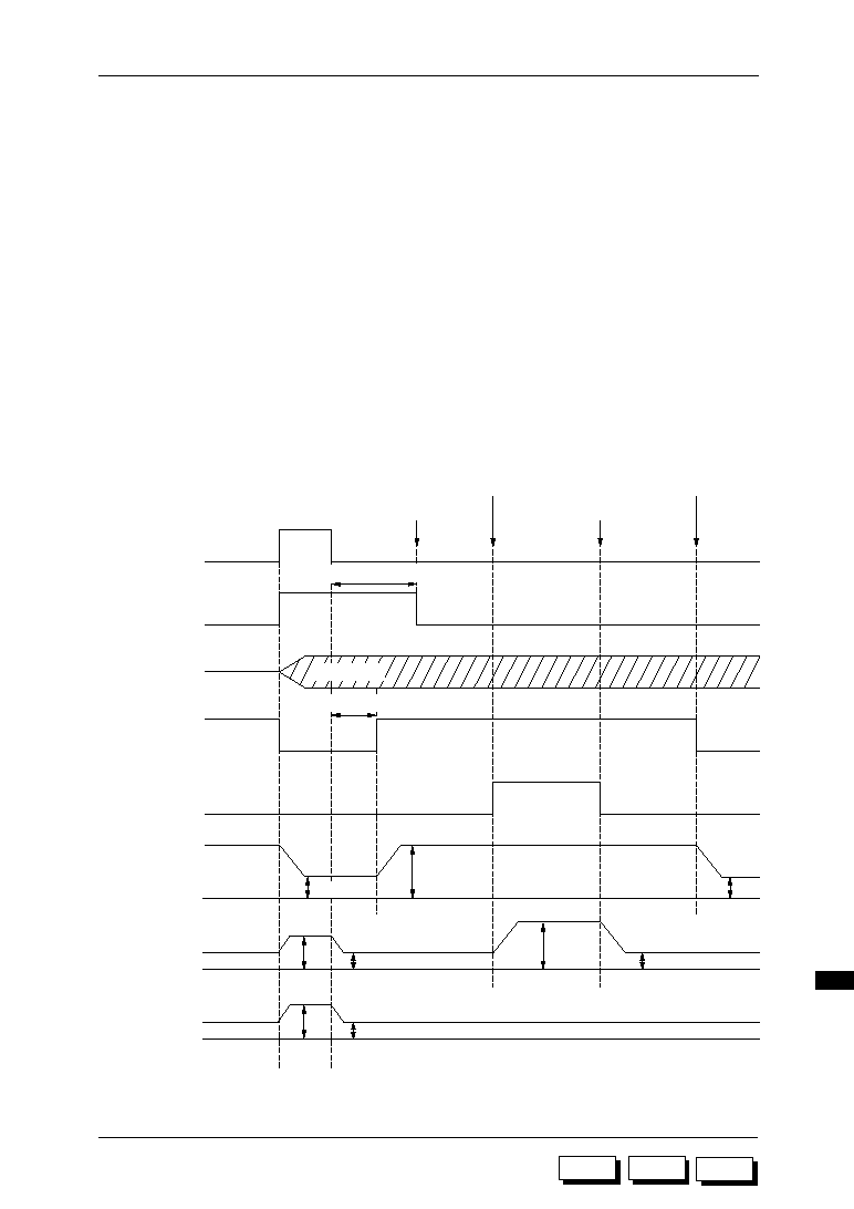
19-5
ML63187/189B/193 User's Manual
Chapter 19 Backup Circuit (BACKUP)
M187
M189B
M193
19
19.4 Power Supply Circuit Operation
When the backup circuit is used, the V
DDH
output is forcibly switched to the V
DD
level while
the time base counter is reset (RESET0 = "1"). Approximately 62.5 ms after system reset is
released, the backup circuit is turned ON, and the V
DDH
output is boosted to twice the V
DD
level. When the backup circuit is turned OFF, the V
DDH
output immediately returns to the V
DD
level.
When the backup circuit is not used, externally connect the V
DDH
output to the V
DD
pin.
The V
DDL
output is forcibly switched to the V
DD
level while the time base counter is reset, and
changes to approximately 1.5 V immediately after reset is released. If ENOSC (bit 1 of FCON)
is set to "1", the V
DDL
output switches to the V
DDH
level. If ENOSC is cleared to "0", the V
DDL
output returns to approximately 1.5 V.
The V
DD2
output (bias reference voltage for LCDs) is forcibly switched to the V
DD
level while
the time base counter is reset, and outputs the voltage (1.8 to 2.4 V) selected by the display
control register (DSPCNT) after reset is released.
RESETS
(system reset)
Low-speed clock
oscillation output
BACKUP
ENOSC
V
DDH
RESET0 (time base
counter reset)
CPU start
Backup circuit OFF
Stop high-speed oscillation
Start of
high-speed oscillation
V
DDL
V
DD2
V
DD
V
DD
Approx. 1.5 V
Approx. 1.8 to 2.4 V
Approx. 1.5 V
V
DD
V
DDH
32.768 kHz
Approx. 62.5 ms
Approx. V
DD
• 2
Approx. 125 ms
V
DD
Figure 19-3 Power Supply Circuit Operation Waveforms

19-6
ML63187/189B/193 User's Manual
Chapter 19 Backup Circuit (BACKUP)
M187
M189B
M193

M187
M189B
M193
Appendixes

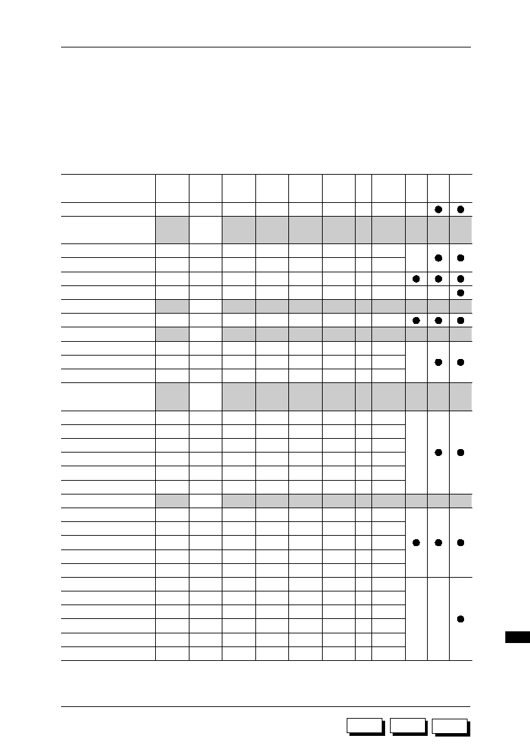
Appendix-1
ML63187/189B/193 User's Manual
Appendix A
M187
M189B
M193
Appendix A List of Special Function Registers
The Special Function Registers of the ML63187, ML63189B, and ML63193 are listed in Table A.
The solid black circles (
l
) indicate that the device is provided with the particular register.
The solid lines (--) indicate that the device is not provided with the particular register.
Table A Special Function Register List
Register name
R/W
Port 0 data register
R
Reserved
Port 9 data register
R/W
Port A data register
R/W
Port B data register
R/W
Port E data register
R/W
Reserved
Port 0 control register 0
R/W
Port 0 control register 1
R/W
Port 0 interrupt enable register
R/W
Reserved
Port 9 control register 0
R/W
Port 9 control register 1
R/W
Port 9 direction register
R/W
Port A control register 0
R/W
Port A control register 1
R/W
Port A direction register
Reserved
R/W
Port B control register 0
Port B control register 1
R/W
Port B direction register
R/W
Port B interrupt enable register
R/W
Port B mode register
R/W
R/W
ML
63187
--
--
--
--
ML
63189B
Symbol
P0D
P9D
PAD
PBD
PED
P0CON0
P0CON1
P0IE
P9CON0
P9CON1
P9DIR
PACON0
PACON1
PADIR
PBCON0
PBCON1
PBDIR
PBIE
PBMOD
Address
000H
001H
to
008H
009H
00AH
00BH
00EH
00FH
010H
011H
012H
013H
to
026H
027H
028H
029H
02AH
02BH
02CH
02DH
02EH
02FH
030H
031H
032H
bit 3
P03
P93
PA3
PB3
PE3
P03MD
--
P03IE
P91MD1
P93MD1
P93DIR
PA1MD1
PA3MD1
PA3DIR
PB1MD1
PB3MD1
PB3DIR
PB3IE
PBF
Undefined
Initial value
at system
reset
0H
0H
0H
0H
0H
0CH
0H
0H
0H
0H
0H
0H
0H
0H
0H
0H
0H
4H
bit 2
P02
P92
PA2
PB2
PE2
P02MD
--
P02IE
P91MD0
P93MD0
P92DIR
PA1MD0
PA3MD0
PA2DIR
PB1MD0
PB3MD0
PB2DIR
PB2IE
--
bit 1
P01
P91
PA1
PB1
PE1
P01MD
P0PUD
P01IE
P90MD1
P92MD1
P91DIR
PA0MD1
PA2MD1
PA1DIR
PB0MD1
PB2MD1
PB1DIR
PB1IE
PB1MOD
bit 0
P00
P90
PA0
PB0
PE0
P00MD
P0F
P00IE
P90MD0
P92MD0
P90DIR
PA0MD0
PA2MD0
PA0DIR
PB0MD0
PB2MD0
PB0DIR
PB0IE
PB0MOD
ML
63193
Port C data register
R/W
PCD
00CH
PC3
0H
PC2
PC1
PC0
Reserved
00DH
--
--
Port C control register 0
Port C control register 1
R/W
Port C direction register
R/W
Port C interrupt enable register
R/W
Port C mode register 0
R/W
R/W
PCCON0
PCCON1
PCDIR
PCIE
PCMOD0
033H
034H
035H
036H
037H
PC1MD1
PC3MD1
PC3DIR
PC3IE
--
0H
0H
0H
0H
0EH
PC1MD0
PC3MD0
PC2DIR
PC2IE
--
PC0MD1
PC2MD1
PC1DIR
PC1IE
--
PC0MD0
PC2MD0
PC0DIR
PC0IE
PCF
Port C mode register 1
R/W
PCMOD1
038H
PC3MOD
0H
PC2MOD
PC1MOD
PC0MOD
--
--

Appendix-2
ML63187/189B/193 User's Manual
Appendix A
M187
M189B
M193
Table A Special Function Register List (continued)
Register name
R/W
Reserved
Initial value
at system
reset
Interrupt enable register 0
R/W
9H
Interrupt enable register 1
R/W
0EH
6H
Interrupt enable register 2
R/W
0H
Interrupt enable register 3
R/W
3H
Interrupt enable register 4
R/W
0H
Interrupt request register 0
R/W
8H
Interrupt request register 1
R/W
0EH
6H
Interrupt request register 2
R/W
0H
Interrupt request register 3
R/W
3H
Interrupt request register 4
R/W
0H
Reserved
Time base counter register 0
R/W
0H
Time base counter register 1
R/W
0H
Frequency control register
R/W
8H
Reserved
100 Hz timer counter register
R/W Undefined
10 Hz timer counter register
R/W
0H
100 Hz timer counter control register
R/W
0EH
Reserved
Timer 0 data register L
R/W
0H
Timer 0 data register H
R/W
0H
Timer 1 data register L
R/W
0H
Timer 1 data register H
R/W
0H
ML
63187
--
--
ML
63189B
--
--
Symbol
IE0
IE1
IE2
IE3
IE4
IRQ0
IRQ1
IRQ2
IRQ3
IRQ4
TBCR0
TBCR1
FCON
T100CR
T10CR
T100CON
TM0DL
TM0DH
TM1DL
TM1DH
Address
041H
to
04FH
050H
051H
052H
053H
054H
055H
056H
057H
058H
059H
05AH
to
05FH
060H
061H
062H
063H
064H
065H
066H
067H
068H
069H
06AH
06BH
bit 3
--
--
EXI5
ETM3
E10Hz
E2Hz
Q2Hz
--
--
QXI5
QTM3
Q10Hz
16Hz
1Hz
--
100C3
10C3
--
T0D3
T0D7
T1D3
T1D7
bit 2
EXI0
--
--
ETM2
ESFT
E4Hz
Q4Hz
QXI0
--
--
QTM2
QSFT
32Hz
2Hz
OSCSEL
100C2
10C2
--
T0D2
T0D6
T1D2
T1D6
bit 1
EMD
--
--
ETM1
--
E16Hz
Q16Hz
QMD
--
--
QTM1
--
64Hz
4Hz
ENOSC
100C1
10C1
--
T0D1
T0D5
T1D1
T1D5
bit 0
--
EXI2
EXI2
ETM0
--
E32Hz
Q32Hz
QWDT
QXI2
QXI2
QTM0
--
128Hz
8Hz
CPUCLK
100C0
10C0
ECNT
T0D0
T0D4
T1D0
T1D4
ML
63193
--
--
1H
--
EXI1
EXI0
EMD
--
--
--
0H
--
E10Hz
ESFT
EST
ESR
--
--
0H
QXI1
QXI0
QMD
QWDT
--
--
--
0H
Q10Hz
QSFT
QST
QSR
--
--
--
Reserved
Port E control register 0
R/W
Port E control register 1
R/W
Port B direction register
R/W
Port E mode register
PECON0
PECON1
PEDIR
PEMOD
039H
to
03CH
03DH
03EH
03FH
040H
PE1MD1
PE3MD1
PE3DIR
PEF
R/W
0H
0H
0H
0H
PE1MD0
PE3MD0
PE2DIR
PE2MOD
PE0MD1
PE2MD1
PE1DIR
PE1MOD
PE0MD0
PE2MD0
PE0DIR
PE0MOD

Appendix-3
ML63187/189B/193 User's Manual
Appendix A
M187
M189B
M193
Table A Special Function Register List (continued)
Reserved
08FH
Register name
R/W
Timer 2 data register L
R/W
0H
Initial value
at system
reset
Timer 2 data register H
R/W
0H
Timer 3 data register L
R/W
0H
Timer 3 data register H
Timer 2 counter register L
Timer 2 counter register H
Timer 3 counter register L
Timer 3 counter register H
Timer 2 control register 0
Timer 2 control register 1
Timer 2 status register
Timer 3 status register
Timer 3 control register 0
Timer 3 control register 1
R/W
0H
R/W
0H
R/W
0H
R/W
0H
R/W
0H
R/W
0AH
R/W
0CH
R/W
0EH
R/W
0CH
R
0EH
R
0EH
Reserved
Display control register 0
R/W
0H
Display control register 1
R/W
0H
Display contrast register
R/W
0H
Reserved
ML
63187
ML
63189B
Symbol
TM2DL
TM2DH
TM3DL
TM3DH
TM2CL
TM2CH
TM3CL
TM3CH
TM2CON0
TM2CON1
TM2STAT
TM3STAT
TM3CON0
TM3CON1
DSPCON0
DSPCON1
DSPCNT
Address
076H
077H
078H
079H
07AH
07BH
07CH
07DH
07EH
07FH
080H
081H
082H
083H
084H
and
085H
090H
091H
092H
093H
bit 3
T2D3
T2D7
T3D3
T3D7
T2C3
T2C7
T3C3
T3C7
--
--
--
--
--
--
BISEL
DT3
CN3
bit 2
T2D2
T2D6
T3D2
T3D6
T2C2
T2C6
T3C2
T3C6
FMEAS2
--
--
--
--
--
PDWN
DT2
CN2
bit 1
T2D1
T2D5
T3D1
T3D5
T2C1
T2C5
T3C1
T3C5
--
TM2CL1
--
TM3CL1
--
--
ALLON
DT1
CN1
bit 0
T2D0
T2D4
T3D0
T3D4
T2C0
T2C4
T3C0
T3C4
TM2RUN
TM2CL0
TM3RUN
TM3CL0
TM2OVF
TM3OVF
LCDON
DT0
CN0
ML
63193
Multiplication/division
condition register
R/W
0H
C register L
R/W
0H
C register H
R/W
0H
D register L
D register H
E register L
E register H
F register L
R/W
0H
R/W
0H
R/W
0H
R/W
0H
R/W
0H
MDCR
CRL
CRH
DRL
DRH
ERL
ERH
FRL
086H
087H
088H
089H
08AH
08BH
08CH
08DH
OV
CR3
CR7
DR3
DR7
ER3
ER7
FR3
EF
CR2
CR6
DR2
DR6
ER2
ER6
FR2
DIVS
CR1
CR5
DR1
DR5
ER1
ER5
FR1
MULS
CR0
CR4
DR0
DR4
ER0
ER4
FR0
F register H
R/W
0H
FRH
08EH
FR7
FR6
FR5
FR4
--
--
Timer 0 counter register L
R/W
0H
Timer 0 counter register H
R/W
0H
Timer 1 counter register L
R/W
0H
Timer 1 counter register H
R/W
0H
Timer 0 control register 0
R/W
8H
Timer 0 control register 1
R/W
0CH
Timer 1 control register 0
R/W
0CH
Timer 1 control register 1
R/W
0CH
Timer 0 status register
R
0CH
Timer 1 status register
TM0CL
TM0CH
TM1CL
TM1CH
TM0CON0
TM0CON1
TM1CON0
TM1CON1
TM0STAT
TM1STAT
06CH
06DH
06EH
06FH
070H
071H
072H
073H
074H
075H
T0C3
T0C7
T1C3
T1C7
--
--
--
--
--
--
R
0CH
T0C2
T0C6
T1C2
T1C6
FMEAS0
--
--
--
--
--
T0C1
T0C5
T1C1
T1C5
TM0ECAP
TM0CL1
TM1ECAP
TM1CL1
TM0CAP
TM1CAP
T0C0
T0C4
T1C0
T1C4
TM0RUN
TM0CL0
TM1RUN
TM1CL0
TM0OVF
TM1OVF
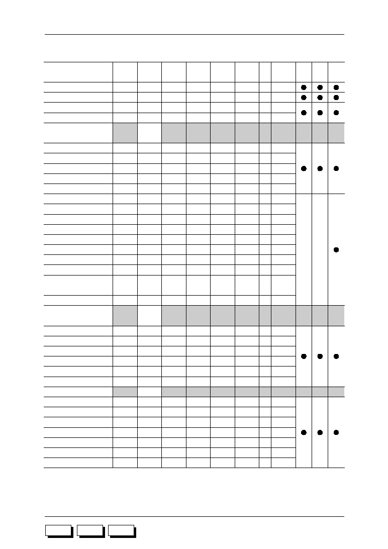
Appendix-4
ML63187/189B/193 User's Manual
Appendix A
M187
M189B
M193
Table A Special Function Register List (continued)
Register name
R/W
Stack pointer
R
0H
Initial value
at system
reset
Reserved
Y register
R/W
0H
X register
R/W
0H
L register
R/W
0H
H register
R/W
0H
ML
63187
ML
63189B
Current bank register
R/W
0H
Extra bank register
R/W
0H
Master interrupt enable flag register
Symbol
SP
Y
X
L
H
CBR
EBR
MIEF
Address
0F7H
0F8H
0F9H
0FAH
0FBH
0FCH
0FDH
0FEH
0FFH
bit 3
sp3
y3
x3
l3
h3
c3
e3
--
R
0EH
bit 2
sp2
y2
x2
l2
h2
c2
e2
--
bit 1
sp1
y1
x1
l1
h1
c1
e1
--
bit 0
sp0
y0
x0
l0
h0
c0
e0
MIE
ML
63193
Battery low detect control register
R/W
0H
Backup control register
R/W
0FH
Tempo register
R/W
0H
Melody driver control register
R/W
0H
Reserved
Watchdog timer control register
W
--
Shift register L
R/W
0H
Shift register H
R/W
0H
Shift register control register 0
R/W
8H
Shift register control register 1
R/W
0EH
Reserved
RA register 0
R/W
0H
RA register 1
R/W
0H
RA register 2
R/W
0H
RA register 3
R/W
0H
Register stack pointer
BLDCON
BUPCON
TEMPO
MDCON
WDTCON
SFTRL
SFTRH
SFTCON0
SFTCON1
RA0
RA1
RA2
RA3
RSP
094H
095H
096H
097H
098H
to
09EH
09FH
0A0H
0A1H
0A2H
0A3H
0AEH
to
0F1H
0F2H
0F3H
0F4H
0F5H
0F6H
BLDF
--
TMP3
MSF
d3
SD3
SD7
--
--
a3
a7
a11
a15
rsp3
R/W
0H
ENBL
--
TMP2
EMBD
d2
SD2
SD6
SDIR
--
a2
a6
a10
a14
rsp2
LD1
--
TMP1
MBM1
d1
SD1
SD5
SELCK1
--
a1
a5
a9
a13
rsp1
LD0
BACKUP
TMP0
MBM0
d0
SD0
SD4
SELCK0
ENTR
a0
a4
a8
a12
rsp0
Serial port send buffer L
R/W
0H
STBUFL
0A4H
TB3
TB2
TB1
TB0
Serial port send buffer H
R/W
0H
STBUFH
0A5H
TB7
TB6
TB5
TB4
Serial port send control register 0
R/W
0H
STCON0
0A6H
STSTB
STL1
STL0
STMOD
Serial port send control register 1
R/W
0H
STCON1
0A7H
STLMB
STPOE
STPEN
STCLK
Serial port receive buffer L
R
0H
SRBUFL
0A8H
RB3
RB2
RB1
RB0
Serial port receive buffer H
R
0H
SRBUFH
0A9H
RB7
RB6
RB5
RB4
Serial port receive control register 0
R/W
0H
SRCON0
0AAH
SREN
SRL1
SRL0
SRMOD
Serial port receive control register 1
R/W
0H
SRCON1
0ABH
SRLMB
SRPOE
SRPEN
SRCLK
Serial port receive baud rate
setting register
R/W
0CH
SRBRT
0ACH
--
--
BRT1
BRT0
Serial port status register
R
0H
SSTAT
0ADH
BFULL
PERR
0ERR
FERR
--
--
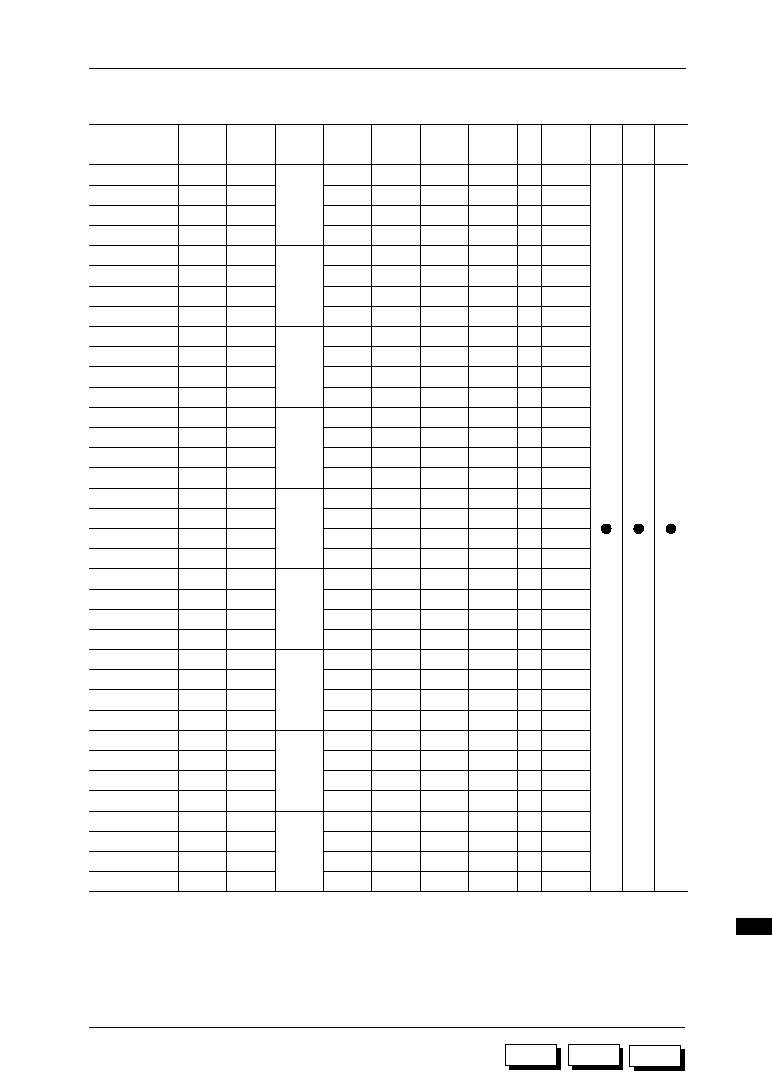
Appendix-5
ML63187/189B/193 User's Manual
Appendix A
M187
M189B
M193
Table A Special Function Register List (continued)
Register name
Symbol
Address
bit 3
bit 2
bit 1
bit 0
R/W
Display register 0
DSPR0
100H
Segment
COM4
R/W Undefined
Initial value
at system
reset
COM3
COM2
COM1
ML
63187
ML
63189B
Display register 1
DSPR1
101H
SEG0
COM8
R/W Undefined
COM7
COM6
COM5
Display register 2
DSPR2
102H
COM12
R/W Undefined
COM11
COM10
COM9
Display register 3
DSPR3
103H
COM16
R/W Undefined
COM15
COM14
COM13
Display register 4
DSPR4
104H
COM4
R/W Undefined
COM3
COM2
COM1
Display register 5
DSPR5
105H
SEG1
COM8
R/W Undefined
COM7
COM6
COM5
Display register 6
DSPR6
106H
COM12
R/W Undefined
COM11
COM10
COM9
Display register 7
DSPR7
107H
COM16
R/W Undefined
COM15
COM14
COM13
Display register 8
DSPR8
108H
COM4
R/W Undefined
COM3
COM2
COM1
Display register 9
DSPR9
109H
SEG2
COM8
R/W Undefined
COM7
COM6
COM5
Display register 10
DSPR10
10AH
COM12
R/W Undefined
COM11
COM10
COM9
Display register 11
DSPR11
10BH
COM16
R/W Undefined
COM15
COM14
COM13
Display register 12
DSPR12
10CH
COM4
R/W Undefined
COM3
COM2
COM1
Display register 13
DSPR13
10DH
SEG3
COM8
R/W Undefined
COM7
COM6
COM5
Display register 14
DSPR14
10EH
COM12
R/W Undefined
COM11
COM10
COM9
Display register 15
DSPR15
10FH
COM16
R/W Undefined
COM15
COM14
COM13
Display register 16
DSPR16
110H
COM4
R/W Undefined
COM3
COM2
COM1
Display register 17
DSPR17
111H
SEG4
COM8
R/W Undefined
COM7
COM6
COM5
Display register 18
DSPR18
112H
COM12
R/W Undefined
COM11
COM10
COM9
Display register 19
DSPR19
113H
COM16
R/W Undefined
COM15
COM14
COM13
Display register 20
DSPR20
114H
COM4
R/W Undefined
COM3
COM2
COM1
Display register 21
DSPR21
115H
SEG5
COM8
R/W Undefined
COM7
COM6
COM5
Display register 22
DSPR22
116H
COM12
R/W Undefined
COM11
COM10
COM9
Display register 23
DSPR23
117H
COM16
R/W Undefined
COM15
COM14
COM13
Display register 24
DSPR24
118H
COM4
R/W Undefined
COM3
COM2
COM1
Display register 25
DSPR25
119H
SEG6
COM8
R/W Undefined
COM7
COM6
COM5
Display register 26
DSPR26
11AH
COM12
R/W Undefined
COM11
COM10
COM9
Display register 27
DSPR27
11BH
COM16
R/W Undefined
COM15
COM14
COM13
Display register 28
DSPR28
11CH
COM4
R/W Undefined
COM3
COM2
COM1
Display register 29
DSPR29
11DH
SEG7
COM8
R/W Undefined
COM7
COM6
COM5
Display register 30
DSPR30
11EH
COM12
R/W Undefined
COM11
COM10
COM9
Display register 31
DSPR31
11FH
COM16
R/W Undefined
COM15
COM14
COM13
Display register 32
DSPR32
120H
COM4
R/W Undefined
COM3
COM2
COM1
Display register 33
DSPR33
121H
SEG8
COM8
R/W Undefined
COM7
COM6
COM5
Display register 34
DSPR34
122H
COM12
R/W Undefined
COM11
COM10
COM9
Display register 35
DSPR35
123H
COM16
R/W Undefined
COM15
COM14
COM13
ML
63193

Appendix-6
ML63187/189B/193 User's Manual
Appendix A
M187
M189B
M193
Table A Special Function Register List (continued)
Register name
Symbol
Address
bit 3
bit 2
bit 1
bit 0
R/W
Display register 36
DSPR36
124H
Segment
COM4
R/W Undefined
Initial value
at system
reset
COM3
COM2
COM1
ML
63187
ML
63189B
Display register 37
DSPR37
125H
SEG9
COM8
R/W Undefined
COM7
COM6
COM5
Display register 38
DSPR38
126H
COM12
R/W Undefined
COM11
COM10
COM9
Display register 39
DSPR39
127H
COM16
R/W Undefined
COM15
COM14
COM13
Display register 40
DSPR40
128H
COM4
R/W Undefined
COM3
COM2
COM1
Display register 41
DSPR41
129H
SEG10
COM8
R/W Undefined
COM7
COM6
COM5
Display register 42
DSPR42
12AH
COM12
R/W Undefined
COM11
COM10
COM9
Display register 43
DSPR43
12BH
COM16
R/W Undefined
COM15
COM14
COM13
Display register 44
DSPR44
12CH
COM4
R/W Undefined
COM3
COM2
COM1
Display register 45
DSPR45
12DH
SEG11
COM8
R/W Undefined
COM7
COM6
COM5
Display register 46
DSPR46
12EH
COM12
R/W Undefined
COM11
COM10
COM9
Display register 47
DSPR47
12FH
130H
131H
132H
133H
134H
135H
136H
137H
138H
139H
13AH
13BH
13CH
13DH
13EH
13FH
140H
141H
142H
143H
144H
145H
146H
147H
COM16
R/W Undefined
COM15
COM14
COM13
Display register 48
DSPR48
COM4
R/W Undefined
COM3
COM2
COM1
Display register 49
DSPR49
SEG12
COM8
R/W Undefined
COM7
COM6
COM5
Display register 50
DSPR50
COM12
R/W Undefined
COM11
COM10
COM9
Display register 51
DSPR51
COM16
R/W Undefined
COM15
COM14
COM13
Display register 52
DSPR52
COM4
R/W Undefined
COM3
COM2
COM1
Display register 53
DSPR53
SEG13
COM8
R/W Undefined
COM7
COM6
COM5
Display register 54
DSPR54
COM12
R/W Undefined
COM11
COM10
COM9
Display register 55
DSPR55
COM16
R/W Undefined
COM15
COM14
COM13
Display register 56
DSPR56
COM4
R/W Undefined
COM3
COM2
COM1
Display register 57
DSPR57
SEG14
COM8
R/W Undefined
COM7
COM6
COM5
Display register 58
DSPR58
COM12
R/W Undefined
COM11
COM10
COM9
Display register 59
DSPR59
COM16
R/W Undefined
COM15
COM14
COM13
Display register 60
DSPR60
COM4
R/W Undefined
COM3
COM2
COM1
Display register 61
DSPR61
SEG15
COM8
R/W Undefined
COM7
COM6
COM5
Display register 62
DSPR62
COM12
R/W Undefined
COM11
COM10
COM9
Display register 63
DSPR63
COM16
R/W Undefined
COM15
COM14
COM13
Display register 64
DSPR64
COM4
R/W Undefined
COM3
COM2
COM1
Display register 65
DSPR65
SEG16
COM8
R/W Undefined
COM7
COM6
COM5
Display register 66
DSPR66
COM12
R/W Undefined
COM11
COM10
COM9
Display register 67
DSPR67
COM16
R/W Undefined
COM15
COM14
COM13
Display register 68
DSPR68
COM4
R/W Undefined
COM3
COM2
COM1
Display register 69
DSPR69
SEG17
COM8
R/W Undefined
COM7
COM6
COM5
Display register 70
DSPR70
COM12
R/W Undefined
COM11
COM10
COM9
Display register 71
DSPR71
COM16
R/W Undefined
COM15
COM14
COM13
ML
63193
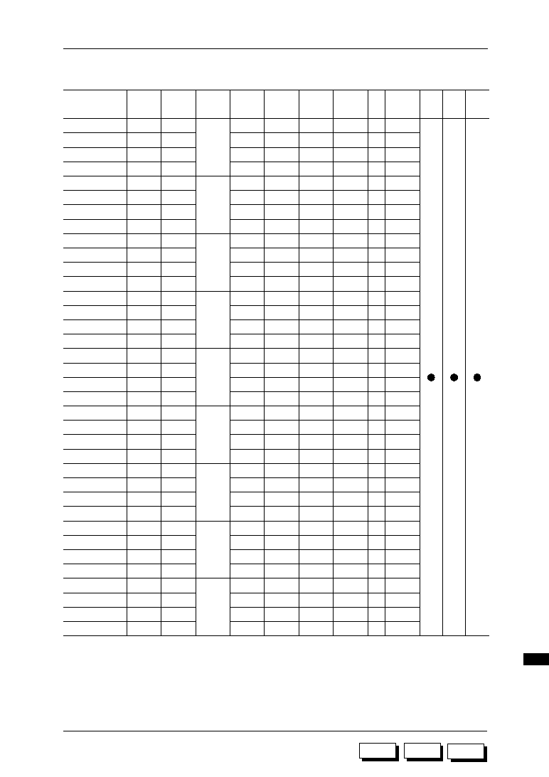
Appendix-7
ML63187/189B/193 User's Manual
Appendix A
M187
M189B
M193
Table A Special Function Register List (continued)
Register name
Symbol
Address
bit 3
bit 2
bit 1
bit 0
R/W
Display register 72
DSPR72
148H
Segment
COM4
R/W Undefined
Initial value
at system
reset
COM3
COM2
COM1
ML
63187
ML
63189B
Display register 73
DSPR73
149H
SEG18
COM8
R/W Undefined
COM7
COM6
COM5
Display register 74
DSPR74
14AH
COM12
R/W Undefined
COM11
COM10
COM9
Display register 75
DSPR75
14BH
COM16
R/W Undefined
COM15
COM14
COM13
Display register 76
DSPR76
14CH
COM4
R/W Undefined
COM3
COM2
COM1
Display register 77
DSPR77
14DH
SEG19
COM8
R/W Undefined
COM7
COM6
COM5
Display register 78
DSPR78
14EH
COM12
R/W Undefined
COM11
COM10
COM9
Display register 79
DSPR79
14FH
COM16
R/W Undefined
COM15
COM14
COM13
Display register 80
DSPR80
150H
COM4
R/W Undefined
COM3
COM2
COM1
Display register 81
DSPR81
151H
SEG20
COM8
R/W Undefined
COM7
COM6
COM5
Display register 82
DSPR82
152H
COM12
R/W Undefined
COM11
COM10
COM9
Display register 83
DSPR83
153H
COM16
R/W Undefined
COM15
COM14
COM13
Display register 84
DSPR84
154H
COM4
R/W Undefined
COM3
COM2
COM1
Display register 85
DSPR85
155H
SEG21
COM8
R/W Undefined
COM7
COM6
COM5
Display register 86
DSPR86
156H
COM12
R/W Undefined
COM11
COM10
COM9
Display register 87
DSPR87
157H
158H
159H
15AH
15BH
168H
169H
16AH
16BH
15CH
15DH
15EH
15FH
160H
161H
162H
163H
164H
165H
166H
167H
COM16
R/W Undefined
COM15
COM14
COM13
Display register 88
DSPR88
COM4
R/W Undefined
COM3
COM2
COM1
Display register 89
DSPR89
SEG22
COM8
R/W Undefined
COM7
COM6
COM5
Display register 90
DSPR90
COM12
R/W Undefined
COM11
COM10
COM9
Display register 91
DSPR91
COM16
R/W Undefined
COM15
COM14
COM13
Display register 92
DSPR92
COM4
R/W Undefined
COM3
COM2
COM1
Display register 93
DSPR93
SEG23
COM8
R/W Undefined
COM7
COM6
COM5
Display register 94
DSPR94
COM12
R/W Undefined
COM11
COM10
COM9
Display register 95
DSPR95
COM16
R/W Undefined
COM15
COM14
COM13
Display register 96
DSPR96
COM4
R/W Undefined
COM3
COM2
COM1
Display register 97
DSPR97
SEG24
COM8
R/W Undefined
COM7
COM6
COM5
Display register 98
DSPR98
COM12
R/W Undefined
COM11
COM10
COM9
Display register 99
DSPR99
COM16
R/W Undefined
COM15
COM14
COM13
Display register 100
DSPR100
COM4
R/W Undefined
COM3
COM2
COM1
Display register 101
DSPR101
SEG25
COM8
R/W Undefined
COM7
COM6
COM5
Display register 102
DSPR102
COM12
R/W Undefined
COM11
COM10
COM9
Display register 103
DSPR103
COM16
R/W Undefined
COM15
COM14
COM13
Display register 104
DSPR104
COM4
R/W Undefined
COM3
COM2
COM1
Display register 105
DSPR105
SEG26
COM8
R/W Undefined
COM7
COM6
COM5
Display register 106
DSPR106
COM12
R/W Undefined
COM11
COM10
COM9
Display register 107
DSPR107
COM16
R/W Undefined
COM15
COM14
COM13
ML
63193

Appendix-8
ML63187/189B/193 User's Manual
Appendix A
M187
M189B
M193
Table A Special Function Register List (continued)
Register name
Symbol
Address
bit 3
bit 2
bit 1
bit 0
R/W
Display register 108
DSPR108
Display register 109
DSPR109
Display register 110
DSPR110
Display register 111
DSPR111
Display register 112
DSPR112
Display register 113
DSPR113
Display register 114
DSPR114
Display register 115
DSPR115
Display register 116
DSPR116
Display register 117
DSPR117
Display register 118
DSPR118
Display register 119
DSPR119
Display register 120
DSPR120
Display register 121
DSPR121
Display register 122
DSPR122
Display register 123
DSPR123
Display register 124
DSPR124
Display register 125
DSPR125
Display register 126
DSPR126
Display register 127
DSPR127
Display register 128
DSPR128
Display register 129
DSPR129
Display register 130
DSPR130
Display register 131
DSPR131
Display register 132
DSPR132
Display register 133
DSPR133
Display register 134
DSPR134
Display register 135
DSPR135
Display register 136
DSPR136
Display register 137
DSPR137
Display register 138
DSPR138
Display register 139
DSPR139
Display register 140
DSPR140
Display register 141
DSPR141
Display register 142
DSPR142
Display register 143
DSPR143
16CH
Segment
COM4
R/W Undefined
Initial value
at system
reset
COM3
COM2
COM1
ML
63187
ML
63189B
SEG27
COM8
R/W Undefined
COM7
COM6
COM5
COM12
R/W Undefined
COM11
COM10
COM9
COM16
R/W Undefined
COM15
COM14
COM13
COM4
R/W Undefined
COM3
COM2
COM1
SEG28
COM8
R/W Undefined
COM7
COM6
COM5
COM12
R/W Undefined
COM11
COM10
COM9
COM16
R/W Undefined
COM15
COM14
COM13
COM4
R/W Undefined
COM3
COM2
COM1
SEG29
COM8
R/W Undefined
COM7
COM6
COM5
COM12
R/W Undefined
COM11
COM10
COM9
COM16
R/W Undefined
COM15
COM14
COM13
COM4
R/W Undefined
COM3
COM2
COM1
SEG30
COM8
R/W Undefined
COM7
COM6
COM5
COM12
R/W Undefined
COM11
COM10
COM9
COM16
R/W Undefined
COM15
COM14
COM13
COM4
R/W Undefined
COM3
COM2
COM1
SEG31
COM8
R/W Undefined
COM7
COM6
COM5
COM12
R/W Undefined
COM11
COM10
COM9
COM16
R/W Undefined
COM15
COM14
COM13
COM4
R/W Undefined
COM3
COM2
COM1
SEG32
COM8
R/W Undefined
COM7
COM6
COM5
COM12
R/W Undefined
COM11
COM10
COM9
COM16
R/W Undefined
COM15
COM14
COM13
COM4
R/W Undefined
COM3
COM2
COM1
SEG33
COM8
R/W Undefined
COM7
COM6
COM5
COM12
R/W Undefined
COM11
COM10
COM9
COM16
R/W Undefined
COM15
COM14
COM13
COM4
R/W Undefined
COM3
COM2
COM1
SEG34
COM8
R/W Undefined
COM7
COM6
COM5
COM12
R/W Undefined
COM11
COM10
COM9
COM16
R/W Undefined
COM15
COM14
COM13
COM4
R/W Undefined
COM3
COM2
COM1
SEG35
COM8
R/W Undefined
COM7
COM6
COM5
COM12
R/W Undefined
COM11
COM10
COM9
COM16
R/W Undefined
COM15
COM14
COM13
16DH
16EH
16FH
170H
171H
172H
173H
174H
175H
176H
177H
178H
179H
17AH
17BH
17CH
17DH
17EH
17FH
180H
181H
182H
183H
184H
185H
186H
187H
188H
189H
18AH
18BH
18CH
18DH
18EH
18FH
ML
63193

Appendix-9
ML63187/189B/193 User's Manual
Appendix A
M187
M189B
M193
Table A Special Function Register List (continued)
Register name
Symbol
Address
bit 3
bit 2
bit 1
bit 0
R/W
Display register 144
DSPR144
Display register 145
DSPR145
Display register 146
DSPR146
Display register 147
DSPR147
Display register 148
DSPR148
Display register 149
DSPR149
Display register 150
DSPR150
Display register 151
DSPR151
Display register 152
DSPR152
Display register 153
DSPR153
Display register 154
DSPR154
Display register 155
DSPR155
Display register 156
DSPR156
Display register 157
DSPR157
Display register 158
DSPR158
Display register 159
DSPR159
Display register 160
DSPR160
Display register 161
DSPR161
Display register 162
DSPR162
Display register 163
DSPR163
Display register 164
DSPR164
Display register 165
DSPR165
Display register 166
DSPR166
Display register 167
DSPR167
Display register 168
DSPR168
Display register 169
DSPR169
Display register 170
DSPR170
Display register 171
DSPR171
Display register 172
DSPR172
Display register 173
DSPR173
Display register 174
DSPR174
Display register 175
DSPR175
Display register 176
DSPR176
Display register 177
DSPR177
Display register 178
DSPR178
Display register 179
DSPR179
Segment
COM4
R/W Undefined
Initial value
at system
reset
COM3
COM2
COM1
ML
63187
ML
63189B
SEG36
COM8
R/W Undefined
COM7
COM6
COM5
COM12
R/W Undefined
COM11
COM10
COM9
COM16
R/W Undefined
COM15
COM14
COM13
COM4
R/W Undefined
COM3
COM2
COM1
SEG37
COM8
R/W Undefined
COM7
COM6
COM5
COM12
R/W Undefined
COM11
COM10
COM9
COM16
R/W Undefined
COM15
COM14
COM13
COM4
R/W Undefined
COM3
COM2
COM1
SEG38
COM8
R/W Undefined
COM7
COM6
COM5
COM12
R/W Undefined
COM11
COM10
COM9
COM16
R/W Undefined
COM15
COM14
COM13
COM4
R/W Undefined
COM3
COM2
COM1
SEG39
COM8
R/W Undefined
COM7
COM6
COM5
COM12
R/W Undefined
COM11
COM10
COM9
COM16
R/W Undefined
COM15
COM14
COM13
COM4
R/W Undefined
COM3
COM2
COM1
SEG40
COM8
R/W Undefined
COM7
COM6
COM5
COM12
R/W Undefined
COM11
COM10
COM9
COM16
R/W Undefined
COM15
COM14
COM13
COM4
R/W Undefined
COM3
COM2
COM1
SEG41
COM8
R/W Undefined
COM7
COM6
COM5
COM12
R/W Undefined
COM11
COM10
COM9
COM16
R/W Undefined
COM15
COM14
COM13
COM4
R/W Undefined
COM3
COM2
COM1
SEG42
COM8
R/W Undefined
COM7
COM6
COM5
COM12
R/W Undefined
COM11
COM10
COM9
COM16
R/W Undefined
COM15
COM14
COM13
COM4
R/W Undefined
COM3
COM2
COM1
SEG43
COM8
R/W Undefined
COM7
COM6
COM5
COM12
R/W Undefined
COM11
COM10
COM9
COM16
R/W Undefined
COM15
COM14
COM13
COM4
R/W Undefined
COM3
COM2
COM1
SEG44
COM8
R/W Undefined
COM7
COM6
COM5
COM12
R/W Undefined
COM11
COM10
COM9
COM16
R/W Undefined
COM15
COM14
COM13
190H
191H
192H
193H
194H
195H
196H
197H
198H
199H
19AH
19BH
19CH
19DH
19EH
19FH
1A0H
1A1H
1A2H
1A3H
1A4H
1A5H
1A6H
1A7H
1A8H
1A9H
1AAH
1ABH
1ACH
1ADH
1AEH
1AFH
1B0H
1B1H
1B2H
1B3H
ML
63193
Appendix-10
ML63187/189B/193 User's Manual
Appendix A
M187
M189B
M193
Table A Special Function Register List (continued)
Register name
Symbol
Address
bit 3
bit 2
bit 1
bit 0
R/W
Display register 180
DSPR180
Display register 181
DSPR181
Display register 182
DSPR182
Display register 183
DSPR183
Display register 184
DSPR184
Display register 185
DSPR185
Display register 186
DSPR186
Display register 187
DSPR187
Display register 188
DSPR188
Display register 189
DSPR189
Display register 190
DSPR190
Display register 191
DSPR191
Display register 192
DSPR192
Display register 193
DSPR193
Display register 194
DSPR194
Display register 195
DSPR195
Display register 196
DSPR196
Display register 197
DSPR197
Display register 198
DSPR198
Display register 199
DSPR199
Display register 200
DSPR200
Display register 201
DSPR201
Display register 202
DSPR202
Display register 203
DSPR203
Display register 204
DSPR204
Display register 205
DSPR205
Display register 206
DSPR206
Display register 207
DSPR207
Display register 208
DSPR208
Display register 209
DSPR209
Display register 210
DSPR210
Display register 211
DSPR211
Display register 212
DSPR212
Display register 213
DSPR213
Display register 214
DSPR214
Display register 215
DSPR215
Segment
COM4
R/W Undefined
Initial value
at system
reset
COM3
COM2
COM1
ML
63187
ML
63189B
SEG45
COM8
R/W Undefined
COM7
COM6
COM5
COM12
R/W Undefined
COM11
COM10
COM9
COM16
R/W Undefined
COM15
COM14
COM13
COM4
R/W Undefined
COM3
COM2
COM1
SEG46
COM8
R/W Undefined
COM7
COM6
COM5
COM12
R/W Undefined
COM11
COM10
COM9
COM16
R/W Undefined
COM15
COM14
COM13
COM4
R/W Undefined
COM3
COM2
COM1
SEG47
COM8
R/W Undefined
COM7
COM6
COM5
COM12
R/W Undefined
COM11
COM10
COM9
COM16
R/W Undefined
COM15
COM14
COM13
COM4
R/W Undefined
COM3
COM2
COM1
SEG48
COM8
R/W Undefined
COM7
COM6
COM5
COM12
R/W Undefined
COM11
COM10
COM9
COM16
R/W Undefined
COM15
COM14
COM13
COM4
R/W Undefined
COM3
COM2
COM1
SEG49
COM8
R/W Undefined
COM7
COM6
COM5
COM12
R/W Undefined
COM11
COM10
COM9
COM16
R/W Undefined
COM15
COM14
COM13
COM4
R/W Undefined
COM3
COM2
COM1
SEG50
COM8
R/W Undefined
COM7
COM6
COM5
COM12
R/W Undefined
COM11
COM10
COM9
COM16
R/W Undefined
COM15
COM14
COM13
COM4
R/W Undefined
COM3
COM2
COM1
SEG51
COM8
R/W Undefined
COM7
COM6
COM5
COM12
R/W Undefined
COM11
COM10
COM9
COM16
R/W Undefined
COM15
COM14
COM13
COM4
R/W Undefined
COM3
COM2
COM1
SEG52
COM8
R/W Undefined
COM7
COM6
COM5
COM12
R/W Undefined
COM11
COM10
COM9
COM16
R/W Undefined
COM15
COM14
COM13
COM4
R/W Undefined
COM3
COM2
COM1
SEG53
COM8
R/W Undefined
COM7
COM6
COM5
COM12
R/W Undefined
COM11
COM10
COM9
COM16
R/W Undefined
COM15
COM14
COM13
1B4H
1B5H
1B6H
1B7H
1B8H
1B9H
1BAH
1BBH
1BCH
1BDH
1BEH
1BFH
1C0H
1C1H
1C2H
1C3H
1C4H
1C5H
1C6H
1C7H
1C8H
1C9H
1CAH
1CBH
1CCH
1CDH
1CEH
1CFH
1D0H
1D1H
1D2H
1D3H
1D4H
1D5H
1D6H
1D7H
ML
63193
Appendix-11
ML63187/189B/193 User's Manual
Appendix A
M187
M189B
M193
Table A Special Function Register List (continued)
Register name
Symbol
Address
bit 3
bit 2
bit 1
bit 0
R/W
Display register 216
DSPR216
Display register 217
DSPR217
Display register 218
DSPR218
Display register 219
DSPR219
Display register 220
DSPR220
Display register 221
DSPR221
Display register 222
DSPR222
Display register 223
DSPR223
Display register 224
DSPR224
Display register 225
DSPR225
Display register 226
DSPR226
Display register 227
DSPR227
Display register 228
DSPR228
Display register 229
DSPR229
Display register 230
DSPR230
Display register 231
DSPR231
Display register 232
DSPR232
Display register 233
DSPR233
Display register 234
DSPR234
Display register 235
DSPR235
Display register 236
DSPR236
Display register 237
DSPR237
Display register 238
DSPR238
Display register 239
DSPR239
Display register 240
DSPR240
Display register 241
DSPR241
Display register 242
DSPR242
Display register 243
DSPR243
Display register 244
DSPR244
Display register 245
DSPR245
Display register 246
DSPR246
Display register 247
DSPR247
Display register 248
DSPR248
Display register 249
DSPR249
Display register 250
DSPR250
Display register 251
DSPR251
Segment
COM4
R/W Undefined
Initial value
at system
reset
COM3
COM2
COM1
ML
63187
ML
63189B
SEG54
COM8
R/W Undefined
COM7
COM6
COM5
COM12
R/W Undefined
COM11
COM10
COM9
COM16
R/W Undefined
COM15
COM14
COM13
COM4
R/W Undefined
COM3
COM2
COM1
SEG55
COM8
R/W Undefined
COM7
COM6
COM5
COM12
R/W Undefined
COM11
COM10
COM9
COM16
R/W Undefined
COM15
COM14
COM13
COM4
R/W Undefined
COM3
COM2
COM1
SEG56
COM8
R/W Undefined
COM7
COM6
COM5
COM12
R/W Undefined
COM11
COM10
COM9
COM16
R/W Undefined
COM15
COM14
COM13
COM4
R/W Undefined
COM3
COM2
COM1
SEG57
COM8
R/W Undefined
COM7
COM6
COM5
COM12
R/W Undefined
COM11
COM10
COM9
COM16
R/W Undefined
COM15
COM14
COM13
COM4
R/W Undefined
COM3
COM2
COM1
SEG58
COM8
R/W Undefined
COM7
COM6
COM5
COM12
R/W Undefined
COM11
COM10
COM9
COM16
R/W Undefined
COM15
COM14
COM13
COM4
R/W Undefined
COM3
COM2
COM1
SEG59
COM8
R/W Undefined
COM7
COM6
COM5
COM12
R/W Undefined
COM11
COM10
COM9
COM16
R/W Undefined
COM15
COM14
COM13
COM4
R/W Undefined
COM3
COM2
COM1
SEG60
COM8
R/W Undefined
COM7
COM6
COM5
COM12
R/W Undefined
COM11
COM10
COM9
COM16
R/W Undefined
COM15
COM14
COM13
COM4
R/W Undefined
COM3
COM2
COM1
SEG61
COM8
R/W Undefined
COM7
COM6
COM5
COM12
R/W Undefined
COM11
COM10
COM9
COM16
R/W Undefined
COM15
COM14
COM13
COM4
R/W Undefined
COM3
COM2
COM1
SEG62
COM8
R/W Undefined
COM7
COM6
COM5
COM12
R/W Undefined
COM11
COM10
COM9
COM16
R/W Undefined
COM15
COM14
COM13
1D8H
1D9H
1DAH
1DBH
1DCH
1DDH
1DEH
1DFH
1E0H
1E1H
1E2H
1E3H
1E4H
1E5H
1E6H
1E7H
1E8H
1E9H
1EAH
1EBH
1ECH
1EDH
1EEH
1EFH
1F0H
1F1H
1F2H
1F3H
1F4H
1F5H
1F6H
1F7H
1F8H
1F9H
1FAH
1FBH
Display register 252
DSPR252
Display register 253
DSPR253
Display register 254
DSPR254
Display register 255
DSPR255
COM4
R/W Undefined
COM3
COM2
COM1
SEG63
COM8
R/W Undefined
COM7
COM6
COM5
COM12
R/W Undefined
COM11
COM10
COM9
COM16
R/W Undefined
COM15
COM14
COM13
1FCH
1FDH
1FEH
1FFH
ML
63193

Appendix-12
ML63187/189B/193 User's Manual
Appendix B
M187
M189B
M193
Appendix B Package Dimensions
(Unit : mm)
ML63187-xxxGA
ML63189B-xxxGA
Mirror finish
Figure B-1 128-Pin QFP (QFP128-P-1420-0.50-K)
Notes for Mounting the Surface Mount Type Package
The SOP, QFP, TSOP, TQFP, LQFP, SOJ, QFJ (PLCC), SHP, and BGA are surface mount
type packages, which are very susceptible to heat in reflow mounting and humidity absorbed
in storage. Therefore, before you perform reflow mounting, contact Oki's responsible sales
person on the product name, package name, pin number, package code and desired
mounting conditions (reflow method, temperature, and times).
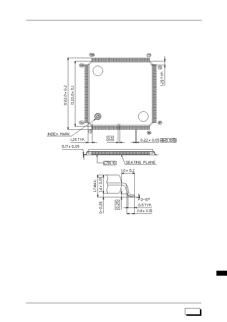
Appendix-13
ML63187/189B/193 User's Manual
Appendix B
M187
M189B
M193
(Unit : mm)
ML63193-xxxTC
Figure B-2 144-Pin LQFP (LQFP144-P-2020-0.50-K)
Notes for Mounting the Surface Mount Type Package
The SOP, QFP, TSOP, TQFP, LQFP, SOJ, QFJ (PLCC), SHP, and BGA are surface mount
type packages, which are very susceptible to heat in reflow mounting and humidity absorbed
in storage. Therefore, before you perform reflow mounting, contact Oki's responsible sales
person on the product name, package name, pin number, package code and desired
mounting conditions (reflow method, temperature, and times).
Mirror finish

Appendix-14
ML63187/189B/193 User's Manual
Appendix C
M187
M189B
M193
Appendix C Input/Output Circuit Configuration
(1) I/O Port (P9.0≠P9.3, PA.0≠PA.3, PB.0≠PB.3, PC.0≠PC.3, PE.0≠PE.3)
(2) Input Port (P0.0≠P0.3)
V
SS
V
DDI
V
DDI
V
SS
V
DDI
I/O
Gate
control
circuit
Pull-up/pull-down control
Output data
Output control
Input data
Schmitt trigger input
inside the IC
V
SS
V
DDI
V
DDI
I
Pull-up/pull-down control
Input data
Schmitt trigger input
inside the IC
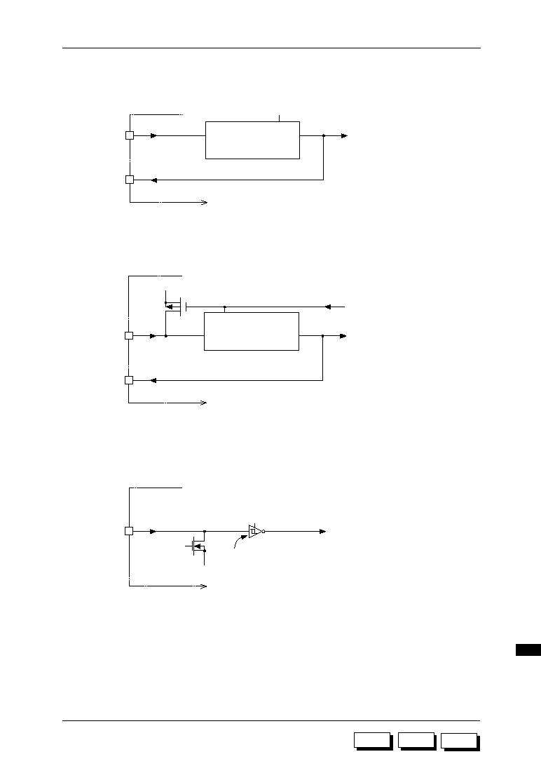
Appendix-15
ML63187/189B/193 User's Manual
Appendix C
M187
M189B
M193
V
DD
I
Schmitt trigger input
V
DD
V
SS
inside the IC
OSC0
V
DDH
OSC1
CMOS input
High-speed clock
(HSCLK)
Oscillation start
inside the IC
(3) Low-Speed Oscillation Circuit
(4) High-Speed Oscillation Circuit
(5) RESET, TST1, and TST2 Inputs
XT0
XT1
CMOS input
Time base clock
(TBCCLK)
inside the IC
V
DDL
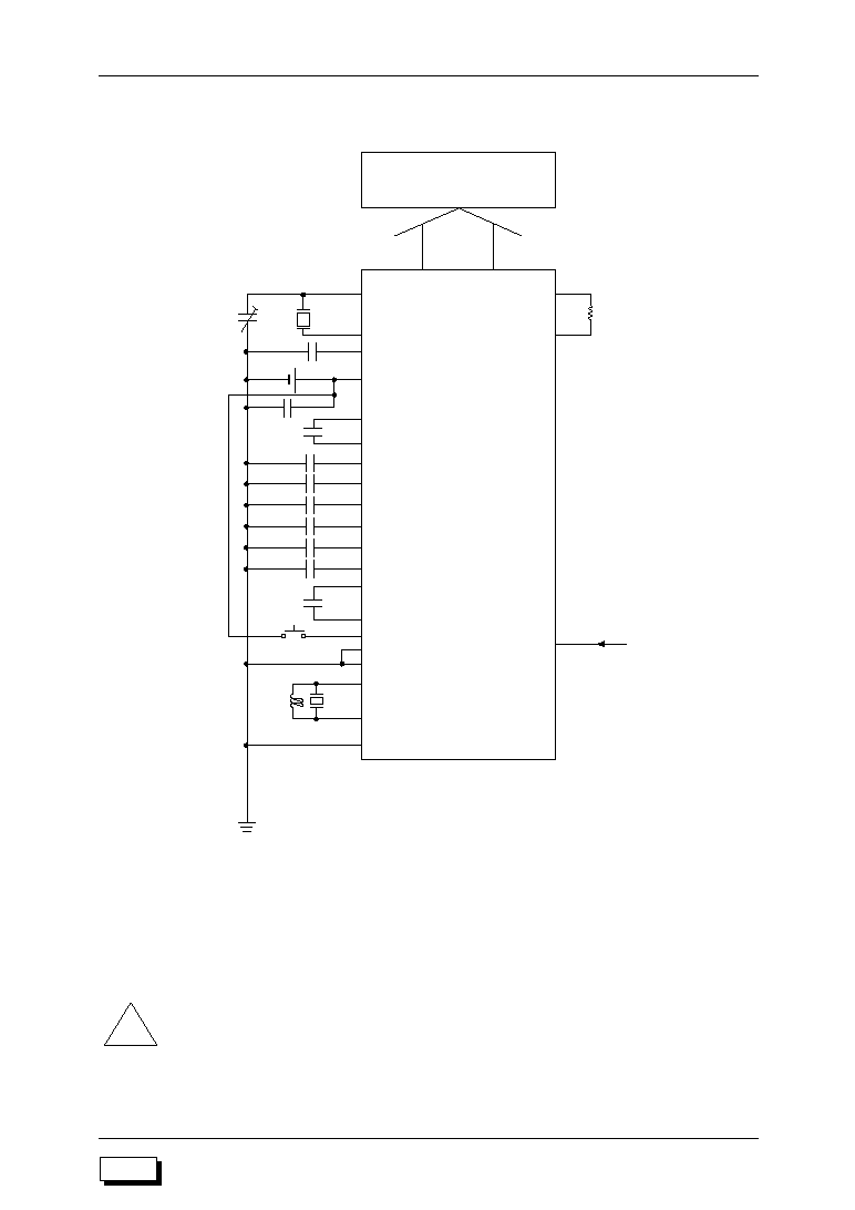
M187
Appendix-16
ML63187/189B/193 User's Manual
Appendix D
Appendix D Peripheral Circuit Examples
Figure D-1 Peripheral Circuit Example with Power Supply Backup
!
Note:
V
DDI
is the power supply pin for input and I/O ports.
V
DDI
must be connected to the positive power supply pin (V
DD
) of the chip or the power supply
pin of the external equipment.
XT0
COM1≠16
XT1
V
DDH
V
DD
CB1
CB2
V
DD5
V
DD4
V
DD3
V
DD2
V
DD1
C1
C2
RESET
TST1
TST2
MD
MDB
V
SS
SEG0≠63
OSC0
OSC1
R
OSH
PB.3
PB.2
PB.1
PB.0
PE.3
PE.2
PE.1
PE.0
C
b12
C
v
C
G
C
12
LCD
32.768 kHz
crystal
C
h
1.5 V
C
e
0.1
mF
C
d
0.1
mF
C
c
0.1
mF
C
b
0.1
mF
C
a
0.1
mF
Buzzer
V
DDI
Push-button switch
ML63187
V
DDL
1.0
mF
0.1
mF
1.0
mF
5 to 25 pF
V
DD
0.1
mF
C
I
0.1
mF
∑ Crystal oscillation is selected by mask option for low-speed oscillation.
∑ RC oscillation is selected for high-speed oscillation.
∑ The power supply for the ports is shared with V
DD
.
∑ C
V
is an IC power supply bypass capacitor.
∑ Capacitance values for C
a
, C
b
, C
c
, C
d
, C
e
, C
l
, C
b12
, C
12
, C
h
, and C
G
are only for
reference.
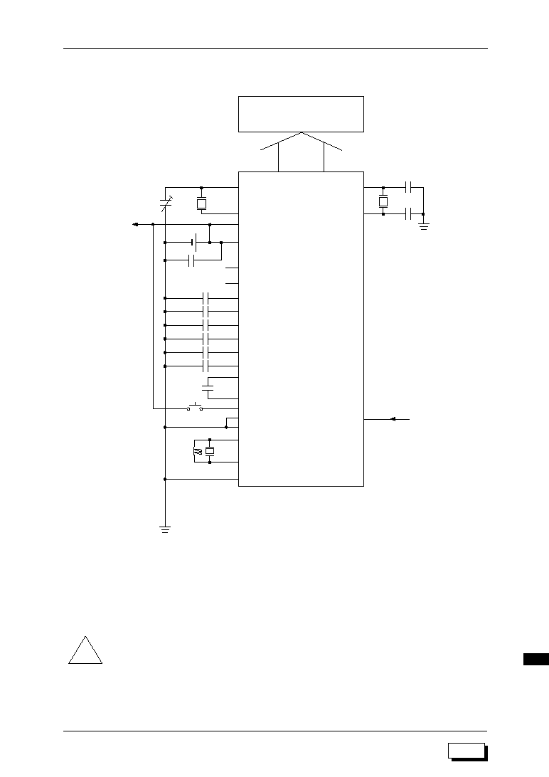
Appendix-17
ML63187/189B/193 User's Manual
Appendix D
M189B
XT0
COM1≠16
XT1
V
DDH
V
DD
CB1
Open
V
DD5
V
DD4
V
DD3
V
DD2
V
DD1
C1
C2
RESET
TST1
TST2
MD
MDB
V
SS
SEG0≠63
OSC0
OSC1
PA.3
PA.2
PA.1
PA.0
PB.3
PB.2
PB.1
PB.0
P0.3
P0.2
P0.1
P0.0
P9.3
P9.2
P9.1
P9.0
C
v
C
G
C
12
LCD
32.768 kHz
crystal
V
DD
5.0 V
C
e
0.1
mF
C
d
0.1
mF
C
c
0.1
mF
C
b
0.1
mF
C
a
0.1
mF
Buzzer
V
DDI
V
DD
C
L0
C
L1
Ceramic resonator
Push-button switch
ML63189B
V
DDL
PE.3
PE.2
PE.1
PE.0
0.1
mF
0.1
mF
5 to 25 pF
CB2
C
l
0.1
mF
Figure D-2 Peripheral Circuit Example with No Backup
!
Note:
V
DDI
is the power supply pin for input and I/O ports.
V
DDI
must be connected to the positive power supply pin (V
DD
) of the chip or the power supply
pin of the external equipment.
∑ Crystal oscillation is selected by mask option for low-speed oscillation.
∑ Ceramic oscillation is selected for high-speed oscillation.
∑ The power supply for the ports is shared with V
DD
.
∑ C
V
is an IC power supply bypass capacitor.
∑ Capacitance values for C
a
, C
b
, C
c
, C
d
, C
e
, C
l
, C
b12
, C
12
, and C
G
are only for reference.
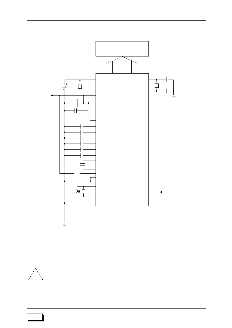
M187
Appendix-18
ML63187/189B/193 User's Manual
Appendix D
XT0
COM1≠16
XT1
V
DDH
V
DD
CB1
Open
V
DD5
V
DD4
V
DD3
V
DD2
V
DD1
C1
C2
RESET
TST1
TST2
MD
MDB
V
SS
SEG0≠63
OSC0
OSC1
PA.3
PA.2
PA.1
PA.0
PB.3
PB.2
PB.1
PB.0
P0.3
P0.2
P0.1
P0.0
P9.3
P9.2
P9.1
P9.0
C
v
C
G
C
12
LCD
32.768 kHz
crystal
V
DD
5.0 V
C
e
0.1
mF
C
d
0.1
mF
C
c
0.1
mF
C
b
0.1
mF
C
a
0.1
mF
Buzzer
V
DDI
V
DD
C
L0
C
L1
Ceramic resonator
Push-button switch
ML63193
V
DDL
PE.3
PE.2
PE.1
PE.0
0.1
mF
0.1
mF
5 to 25 pF
CB2
PC.3
PC.2
PC.1
PC.0
C
l
0.1
mF
Figure D-3 Peripheral Circuit Example with No Backup
!
Note:
V
DDI
is the power supply pin for input and I/O ports.
V
DDI
must be connected to the positive power supply pin (V
DD
) of the chip or the power supply
pin of the external equipment.
M193
∑ Crystal oscillation is selected by mask option for low-speed oscillation.
∑ Ceramic oscillation is selected for high-speed oscillation.
∑ The power supply for the ports is shared with V
DD
.
∑ C
V
is an IC power supply bypass capacitor.
∑ Capacitance values for C
a
, C
b
, C
c
, C
d
, C
e
, C
l
, C
b12
, C
12
, and C
G
are only for reference.
Appendix-19
ML63187/189B/193 User's Manual
Appendix E
M187
M189B
M193
Appendix E Electrical Characteristics
Absolute Maximum Ratings
Parameter
Symbol
Condition
Rating
Unit
≠0.3 to +1.6
Power Supply Voltage 1
Ta = 25∞C
V
DD1
V
≠0.3 to +2.9
Power Supply Voltage 2
Ta = 25∞C
V
DD2
V
≠0.3 to +4.2
Power Supply Voltage 3
Ta = 25∞C
V
DD3
V
≠0.3 to +5.5
Power Supply Voltage 4
Ta = 25∞C
V
DD4
V
≠0.3 to +6.8
Power Supply Voltage 5
Ta = 25∞C
V
DD5
V
Power Supply Voltage 6
V
DD
≠0.3 to +6.0
Power Supply Voltage 7
Ta = 25∞C
V
DDI
V
≠0.3 to +6.0
Power Supply Voltage 8
Ta = 25∞C
V
DDH
V
≠0.3 to V
DD
+ 0.3
Input Voltage 1
V
DD
Input, Ta = 25∞C
V
IN1
V
≠0.3 to V
DDI
+ 0.3
Input Voltage 2
V
DDI
Input, Ta = 25∞C
V
IN2
V
≠0.3 to V
DD1
+ 0.3
Output Voltage 1
V
DD1
Output, Ta = 25∞C
V
OUT1
V
≠0.3 to V
DD2
+ 0.3
Output Voltage 2
V
DD2
Output, Ta = 25∞C
V
OUT2
V
≠0.3 to V
DD3
+ 0.3
Output Voltage 3
V
DD3
Output, Ta = 25∞C
V
OUT3
V
≠0.3 to V
DD4
+ 0.3
Output Voltage 4
V
DD4
Output, Ta = 25∞C
V
OUT4
V
≠0.3 to V
DD5
+ 0.3
Output Voltage 5
V
DD5
Output, Ta = 25∞C
V
OUT5
V
≠0.3 to V
DD
+ 0.3
Output Voltage 6
V
DD
Output, Ta = 25∞C
V
OUT6
V
≠0.3 to V
DDI
+ 0.3
Output Voltage 7
V
DDI
Output, Ta = 25∞C
V
OUT7
V
≠0.3 to V
DDH
+ 0.3
Output Voltage 8
V
DDH
Output, Ta = 25∞C
V
OUT8
V
≠55 to +150
Storage Temperature
--
T
STG
∞C
(V
SS
= 0 V)
≠0.3 to +6.0
Power Supply Voltage 9
Ta = 25∞C
V
DDL
V
≠0.3 to +6.0
Ta = 25∞C
V
Appendix-20
ML63187/189B/193 User's Manual
Appendix E
M187
M189B
M193
V
DDI
0.9 to 5.5
V
Crystal Oscillation Frequency
f
XT
32.768 to 76.8
kHz
Ceramic Oscillation Frequency
f
CM
300k to 500k
V
DD
= 1.2 to 2.7 V
--
C
G
= 5 to 25 pF
Parameter
Symbol
Condition
Range
Unit
Operating Temperature
T
op
≠20 to +70
∞C
V
DD
--
0.9 to 2.7
V
Operating Voltage
(V
SS
= 0 V)
--
High-speed RC Oscillation
Frequency
f
ROSH
200k ±30%
R
OSH
= 100 k
W
Not applied
Hz
V
DD
= 0.9 to 1.2 V
Not applied
Hz
R
OSH
= 400 k
W
Low-speed RC Oscillation
Frequency
f
ROSL
kHz
200k to 1M
V
DD
= 1.5 to 2.7 V
700k ±30%
R
OSH
= 75 k
W
1M ±30%
V
DD
= 0.9 to 1.2 V
60 ±30%
R
OSL
= 700 k
W
32 ±30%
R
OSL
= 1.5 M
W
80 ±30%
R
OSL
= 500 k
W
V
DD
= 1.2 to 2.7 V
Recommended Operating Conditions
∑ When backup is used
V
DDI
1.8 to 5.5
V
Crystal Oscillation Frequency
f
XT
32.768 to 76.8
kHz
Ceramic Oscillation Frequency
f
CM
Hz
--
C
G
= 5 to 25 pF
Parameter
Symbol
Condition
Range
Unit
Operating Temperature
T
op
≠20 to +70
∞C
V
DD
--
1.8 to 5.5
V
Operating Voltage
(V
SS
= 0 V)
--
High-speed RC Oscillation
Frequency
f
ROSH
1M ±30%
Hz
R
OSH
= 75 k
W
1.35M ±30%
R
OSH
= 51 k
W
200k to 2M
V
DD
= 1.8 to 5.5 V
700k ±30%
R
OSH
= 100 k
W
Low-speed RC Oscillation
Frequency
f
ROSL
32 ±30%
kHz
R
OSL
= 1.5 M
W
60 ±30%
R
OSL
= 700 k
W
80 ±30%
R
OSL
= 500 k
W
V
DD
= 1.8 to 5.5 V
V
DD
= 1.8 to 3.5 V, R
OSH
= 30 k
W
2M ±30%
∑ When backup is not used

Appendix-21
ML63187/189B/193 User's Manual
Appendix E
M187
M189B
M193
∑ Typical characteristics of low-speed RC oscillation
When backup is used (V
DD
= V
DDI
= 1.5 V)/backup is not used (V
DD
= V
DDI
= 3.0 V)
∑ Typical characteristics of high-speed RC oscillation
When backup is used (V
DD
= V
DDI
= 1.5 V)
1000
100
10
100
1000
10000
f
ROSL
[kHz]
R
OSL
[k
W]
[Reference data]
10000
1000
100
10
100
1000
f
ROSH
[kHz]
R
OSH
[k
W]
[Reference data]
Appendix-22
ML63187/189B/193 User's Manual
Appendix E
M187
M189B
M193
∑ Typical characteristics of high-speed RC oscillation
When backup is not used (V
DD
= V
DDI
= 3.0 V)
10000
1000
100
10
100
1000
f
ROSH
[kHz]
R
OSH
[k
W]
[Reference data]

Appendix-23
ML63187/189B/193 User's Manual
Appendix E
M187
M189B
M193
DC Characteristics
Parameter
Symbol
Condition
Mea-
suring
Circuit
Unit
1.9
1.8
1.7
V
DD2
Voltage
Max.
Typ.
Min.
V
DD2
1/5 bias, 1/4 bias
(Ta = 25∞C)
V
--
≠4
--
V
DD2
Voltage Temperature Deviation
DV
DD2
--
mV/∞C
Typ.+ 0.3
3/2
• V
DD2
Typ.≠ 0.3
V
DD3
Voltage
V
DD3
1/5 bias
V
Typ.+ 0.4
2
• V
DD2
Typ.≠ 0.4
V
DD4
Voltage
V
DD4
1/5 bias
V
Typ.+ 0.5
5/2
• V
DD2
Typ.≠ 0.5
V
DD5
Voltage
V
DD5
1/5 bias
V
--
--
1.2
Crystal Oscillation Start Voltage
V
STA
Oscillation start time:
within 5 seconds
V
--
--
0.9
Crystal Oscillation Hold Voltage
V
HOLD
Backup used
V
5.0
--
0.1
Crystal Oscillation Stop Detect Time
T
STOP
--
ms
25
--
5
External Crystal Oscillator Capacitance
C
G
--
pF
30
25
20
Internal Crystal Oscillator Capacitance
C
D
--
pF
16
12
8
Internal RC Oscillator Capacitance
C
OS
--
pF
--
30
--
External Ceramic Oscillator
Capacitance
C
L0, 1
CSA2.00MG (Murata
MFG.-make) used
V
DD
= 3.0 V
pF
0.4
--
0.0
POR Voltage
V
POR1
V
DD
= 1.5 V
V
1
0.7
--
0.0
V
DD
= 3.0 V
V
--
--
1.7
Backup not used
V
2.0
1.5
1.0
V
DDL
Voltage
V
DDL
High-speed clock
oscillation stopped
V
5.5
--
1.2
High-speed clock oscillation
(V
DD
= 1.2 to 5.5 V)
V
V
DDH
2.7
--
2.0
V
DDH
Voltage
(Backup used)
High-speed clock oscillation
(Ceramic oscillation, 1 MHz)
V
DD
= 1.5 V
V
High-speed clock oscillation
stopped
V
DD
= 1.5 V
3.0
--
2.8
V
(V
DD
= V
DDI
= 0.9 to 5.5 V, V
SS
= 0 V, Ta = ≠20 to +70∞C unless otherwise specified)
Typ.+ 0.1
1/2
• V
DD2
Typ.≠ 0.1
V
DD1
Voltage
V
DD1
1/5 bias, 1/4 bias
V
Typ.+ 0.2
V
DD2
Typ.≠ 0.2
1/4 bias (connect
V
DD3
and V
DD2
)
Typ.+ 0.3
3/2
• V
DD2
Typ.≠ 0.3
1/4 bias
Typ.+ 0.4
2
• V
DD2
Typ.≠ 0.4
1/4 bias
1.5
--
1.2
Non-POR Voltage
V
POR2
V
DD
= 1.5 V
V
3.0
--
2.0
V
DD
= 3.0 V
V
2.50
2.40
2.30
BLD Judgment Voltage
V
BLDC
LD1 = 1, LD0 = 1, Ta = 25∞C
1.90
1.80
1.70
LD1 = 1, LD0 = 0, Ta = 25∞C
V
1.30
1.20
1.10
LD1 = 0, LD0 = 1, Ta = 25∞C
1.15
1.05
0.95
LD1 = 0, LD0 = 0, Ta = 25∞C
--
--
≠3.5
--
BLD Judgment Voltage
Temperature Deviation
DV
BLDC
V
BLDC
= 2.40 V (LD1 = 1, LD0 = 1)
--
≠2.3
--
V
BLDC
= 1.80 V (LD1 = 1, LD0 = 0)
mV/∞C
--
≠1.6
--
V
BLDC
= 1.20 V (LD1 = 0, LD0 = 1)
--
≠1.2
--
V
BLDC
= 1.05 V (LD1 = 0, LD0 = 0)

Appendix-24
ML63187/189B/193 User's Manual
Appendix E
M187
M189B
M193
Notes: 1. "V
DD2
" voltage varies from 1.8 to 2.4 V depending on the value of the display
contrast register (DSPCNT).
2. "T
STOP
" indicates that if the crystal oscillator stops over the value of T
STOP
, the
system reset occurs.
3. "POR" denotes Power On Reset.
4. "V
POR1
" indicates that POR occurs when V
DD
falls from V
DD
to V
POR1
and again
rises up to V
DD
.
5. "V
POR2
" indicates that POR does not occur when V
DD
falls from V
DD
to V
POR2
and
again rises up to V
DD
.
Appendix-25
ML63187/189B/193 User's Manual
Appendix E
M187
M189B
M193
Parameter
Symbol
Condition
Mea-
suring
Circuit
(32.768 kHz crystal is used for the low-speed clock, V
DD
= V
DDI
= 1.5 V, V
SS
= 0 V, 1/5 bias,
LCD contrast (DSPCNT) = 0H, Ta = ≠20 to +70∞C unless otherwise specified)
Unit
Max.
Typ.
Min.
6.5
5
--
Supply Current 1
I
DD1
CPU is in HALT state.
(High-speed clock oscillation
stopped)
mA
5
4
--
Supply Current 2
I
DD2
CPU is in HALT state.
LCD is in Power Down mode.
(High-speed clock oscillation
stopped)
mA
18
16
--
Supply Current 3
I
DD3
CPU is in operation at
low-speed oscillation.
(High-speed clock oscillation
stopped)
mA
1
10
5
--
8
4
--
Ta = ≠20 to +50∞C
Ta = ≠20 to +50∞C
Ta = ≠20 to +70∞C
Ta = ≠20 to +70∞C
1000
800
--
Supply Current 4
I
DD4
CPU is in operation at high-speed oscillation
(approx.700 kHz RC oscillation, R
OSH
= 100 k
W)
mA
850
700
--
Supply Current 5
I
DD5
CPU is in operation at high-speed oscillation
(Ceramic oscillation, 1 MHz)
mA
Ta = ≠20 to +50∞C
20
16
--
mA
Ta = ≠20 to +70∞C
DC Characteristics (continued)
∑ When backup is used (ML63187/ML63189B)
∑ When backup is not used (ML63187/ML63189B)
Parameter
Symbol
Condition
Mea-
suring
Circuit
(32.768 kHz crystal is used for the low-speed clock, V
DD
= V
DDI
= 3.0 V, V
SS
= 0 V, 1/5 bias,
LCD contrast (DSPCNT) = 0H, Ta = ≠20 to +70∞C unless otherwise specified)
Unit
Max.
Typ.
Min.
3
2.2
--
Supply Current 1
I
DD1
CPU is in HALT state.
(High-speed clock oscillation
stopped)
mA
2.5
1.8
--
Supply Current 2
I
DD2
CPU is in HALT state.
LCD is in Power Down mode.
(High-speed clock oscillation
stopped)
mA
Supply Current 3
I
DD3
1
5
2.2
--
4
1.8
--
Ta = ≠20 to +50∞C
Ta = ≠20 to +50∞C
Ta = ≠20 to +70∞C
Ta = ≠20 to +70∞C
700
550
--
Supply Current 4
I
DD4
CPU is in operation at high-speed oscillation
(approx. 700 kHz RC oscillation, R
OSH
= 100 k
W)
mA
1000
850
--
Supply Current 5
I
DD5
CPU is in operation at high-speed oscillation
(Ceramic oscillation, 2 MHz)
mA
9
7.5
--
CPU is in operation at
low-speed oscillation.
(High-speed clock oscillation
stopped)
mA
12
7.5
--
Ta = ≠20 to +50∞C
Ta = ≠20 to +70∞C
M189B
M187

Appendix-26
ML63187/189B/193 User's Manual
Appendix E
M187
M189B
M193
DC Characteristics (continued)
∑ When backup is used (ML63193)
∑ When backup is not used (ML63193)
Parameter
Symbol
Condition
Mea-
suring
Circuit
(32.768 kHz crystal is used for the low-speed clock, V
DD
= V
DDI
= 1.5 V, V
SS
= 0 V, 1/5 bias,
LCD contrast (DSPCNT) = 0H, Ta = ≠20 to +70∞C unless otherwise specified)
Unit
Max.
Typ.
Min.
6.5
5.6
--
Supply Current 1
I
DD1
CPU is in HALT state.
(High-speed clock oscillation
stopped)
mA
5.0
4.5
--
Supply Current 2
I
DD2
CPU is in HALT state.
LCD is in Power Down mode.
(High-speed clock oscillation
stopped)
mA
26
23
--
Supply Current 3
I
DD3
CPU is in operation at
low-speed oscillation.
(High-speed clock oscillation
stopped)
mA
1
15.0
5.6
--
13.0
4.5
--
Ta = ≠20 to +50∞C
Ta = ≠20 to +50∞C
Ta = ≠20 to +70∞C
Ta = ≠20 to +70∞C
1500
1100
--
Supply Current 4
I
DD4
CPU is in operation at high-speed oscillation
(approx. 700 kHz RC oscillation, R
OSH
= 100 k
W)
mA
1200
950
--
Supply Current 5
I
DD5
CPU is in operation at high-speed oscillation
(Ceramic oscillation, 1 MHz)
mA
Ta = ≠20 to +50∞C
30
23
--
mA
Ta = ≠20 to +70∞C
Parameter
Symbol
Condition
Mea-
suring
Circuit
(32.768 kHz crystal is used for the low-speed clock, V
DD
= V
DDI
= 3.0 V, V
SS
= 0 V, 1/5 bias,
LCD contrast (DSPCNT) = 0H, Ta = ≠20 to +70∞C unless otherwise specified)
Unit
Max.
Typ.
Min.
3.5
2.6
--
Supply Current 1
I
DD1
CPU is in HALT state.
(High-speed clock oscillation
stopped)
mA
2.8
2.0
--
Supply Current 2
I
DD2
CPU is in HALT state.
LCD is in Power Down mode.
(High-speed clock oscillation
stopped)
mA
Supply Current 3
I
DD3
1
7.0
2.6
--
6.0
2.0
--
Ta = ≠20 to +50∞C
Ta = ≠20 to +50∞C
Ta = ≠20 to +70∞C
Ta = ≠20 to +70∞C
1200
1000
--
Supply Current 4
I
DD4
CPU is in operation at high-speed oscillation
(approx. 700 kHz RC oscillation, R
OSH
= 100 k
W)
mA
1300
1100
--
Supply Current 5
I
DD5
CPU is in operation at high-speed oscillation
(Ceramic oscillation, 2 MHz)
mA
13
12
--
CPU is in operation at
low-speed oscillation.
(High-speed clock oscillation
stopped)
mA
16
12
--
Ta = ≠20 to +50∞C
Ta = ≠20 to +70∞C
M193

Appendix-27
ML63187/189B/193 User's Manual
Appendix E
M187
M189B
M193
DC Characteristics (continued)
Parameter
Symbol
Condition
Mea-
suring
Circuit
(V
DD
= V
DDI
= V
DDH
= 3.0 V, V
DD1
= 1.1 V, V
DD2
= 2.2 V, V
DD3
= 3.3 V, V
DD4
= 4.4 V,
V
DD5
= 5.5 V, Ta = ≠20 to +70∞C unless otherwise specified)
Unit
Max.
Output Current 1
(P9.0 to P9.3)*
1
(PA.0 to PA.3)*
1
(PB.0 to PB.3)
(PC.0 to PC.3)*
2
(PE.0 to PE.3)
≠0.4
mA
2
I
OH1
V
OH1
= V
DDI
≠ 0.5 V
≠1.0
mA
≠1.5
mA
Output Current 2
(MD, MDB)
Output Current 4
(OSC1)
I
OH4R
V
OH4R
= V
DDH
≠ 0.5 V
(RC oscillation)
≠0.25
mA
Output Leakage Current
(P9.0 to P9.3)*
1
(PA.0 to PA.3)*
1
(PB.0 to PB.3)
(PC.0 to PC.3)*
2
(PE.0 to PE.3)
I
OOH
V
OH
= V
DDI
0.3
mA
I
OOL
V
OL
= V
SS
--
mA
Typ.
≠1.4
≠3.5
≠5.0
≠1.3
--
--
Min.
≠2.5
≠6.0
≠8.5
≠2.5
--
≠0.3
V
DDI
= 1.5 V
V
DDI
= 3.0 V
V
DDI
= 5.0 V
2.5
mA
I
OL1
V
OL1
= 0.5 V
6.0
mA
8.5
mA
1.4
3.0
3.7
0.4
1.0
1.5
V
DDI
= 1.5 V
V
DDI
= 3.0 V
V
DDI
= 5.0 V
≠0.5
mA
I
OH2
V
OH2
= V
DD
≠ 0.7 V
≠2.0
mA
≠4.0
mA
≠2.0
≠6.0
≠9.0
≠4.0
≠11.0
≠14.0
V
DD
= 1.5 V
V
DD
= 3.0 V
V
DD
= V
DDH
= 5.0 V
4.0
mA
I
OL2
V
OL2
= 0.7 V
11.0
mA
14.0
mA
2.0
5.5
7.0
0.5
2.0
4.0
V
DD
= 1.5 V
V
DD
= 3.0 V
V
DD
= V
DDH
= 5.0 V
Output Current 3
(SEG0 to SEG63)
(COM1 to COM16)
≠4
mA
I
OHM3
--
mA
mA
--
--
--
4
mA
I
OMH3S
mA
mA
V
DD
= V
DDH
= 3.0 V
V
DD
= V
DDH
= 5.0 V
≠0.5
mA
≠1.7
≠3.5
I
OL4R
V
OL4R
= 0.5 V
(RC oscillation)
2.5
mA
1.5
0.25
V
DD
= V
DDH
= 3.0 V
V
DD
= V
DDH
= 5.0 V
3.5
mA
1.8
0.5
I
OH4C
V
OH4C
= V
DDH
≠ 0.5 V
(ceramic oscillation)
≠100
mA
≠250
≠500
V
DD
= V
DDH
= 3.0 V
V
DD
= V
DDH
= 5.0 V
≠200
mA
≠350
≠800
I
OL4C
V
OL4C
= 0.5 V
(ceramic oscillation)
800
mA
500
200
V
DD
= V
DDH
= 3.0 V
V
DD
= V
DDH
= 5.0 V
1000
mA
700
400
I
OH3
V
OH3
= V
DD5
≠ 0.2 V (V
DD5
level)
I
OHM3S
I
OML3
I
OMH3
mA
I
OML3S
mA
I
OLM3
mA
I
OLM3S
mA
I
OL3
V
OHM3
= V
DD4
+ 0.2 V (V
DD4
level)
V
OHM3S
= V
DD4
≠ 0.2 V (V
DD4
level)
V
OMH3
= V
DD3
+ 0.2 V (V
DD3
level)
V
OMH3S
= V
DD3
≠ 0.2 V (V
DD3
level)
V
OML3
= V
DD2
+ 0.2 V (V
DD2
level)
V
OML3S
= V
DD2
≠ 0.2 V (V
DD2
level)
V
OLM3
= V
DD1
+ 0.2 V (V
DD1
level)
V
OLM3S
= V
DD1
≠ 0.2 V (V
DD1
level)
V
OL3
= V
SS
+ 0.2 V (V
SS
level)
≠4
--
--
--
--
4
≠4
--
--
--
--
4
≠4
--
--
--
--
4
≠4
--
--
--
--
4
*1 Applies to the ML63189B and ML63193.
*2 Applies to the ML63193 only.

Appendix-28
ML63187/189B/193 User's Manual
Appendix E
M187
M189B
M193
Parameter
Symbol
Condition
Mea-
suring
Circuit
(V
DD
= V
DDI
= V
DDH
= 3.0 V, V
DD1
= 1.1 V, V
DD2
= 2.2 V, V
DD3
= 3.3 V, V
DD4
= 4.4 V,
V
DD5
= 5.5 V, Ta = ≠20 to +70∞C unless otherwise specified)
Unit
Max.
Input Current 1
(P0.0 to P0.3)*
1
(P9.0 to P9.3)*
1
(PA.0 to PA.3)*
1
(PB.0 to PB.3)
(PC.0 to PC.3)*
2
(PE.0 to PE.3)
45
mA
3
I
IH1
V
IH1
= V
DDI
(when pulled down)
260
mA
650
mA
Input Current 3
(RESET)
I
IH3
V
IH3
= V
DD
350
mA
Typ.
20
120
350
180
Min.
2
30
70
10
V
DDI
= 1.5 V
V
DDI
= 3.0 V
V
DDI
= 5.0 V
≠2
mA
I
IL1
V
IL1
= V
SS
(when pulled up)
≠30
mA
≠70
mA
≠20
≠120
≠350
≠45
≠260
≠650
V
DDI
= 1.5 V
V
DDI
= 3.0 V
V
DDI
= 5.0 V
Input Current 2
(OSC0)
≠30
mA
I
IL2
V
IL2
= V
SS
(when pulled up)
≠200
mA
≠170
≠450
≠350
≠750
V
DD
= V
DDH
= 3.0 V
V
DD
= V
DDH
= 5.0 V
V
DD
= 1.5 V
V
DD
= 3.0 V
2400
mA
1100
150
I
IH1Z
V
IH1
= V
DDI
(in a high impedance state)
1.0
mA
--
0.0
I
IL1Z
V
IL1
= V
SS
(in a high impedance state)
0.0
mA
--
≠1.0
I
IH2R
V
IH2R
= V
DDH
(RC oscillation)
1.0
mA
--
0.0
I
IL2R
V
IL2R
= V
SS
(RC oscillation)
0.0
mA
--
≠1.0
4.0
mA
I
IH2C
V
IH2C
= V
DDH
(ceramic oscillation)
10
mA
1.8
6
0.5
3
V
DD
= V
DDH
= 3.0 V
V
DD
= V
DDH
= 5.0 V
≠0.5
mA
I
IL2C
V
IL2C
= V
SS
(ceramic oscillation)
≠3
mA
≠1.8
≠6
≠4.0
≠10
V
DD
= V
DDH
= 3.0 V
V
DD
= V
DDH
= 5.0 V
V
DD
= V
DDH
= 5.0 V
5.0
mA
2.7
0.5
I
IL3
V
IL3
= V
SS
0.0
mA
--
≠1.0
Input Current 4
(TST1, TST2)
I
IH4
V
IH4
= V
DD
1500
mA
750
50
V
DD
= 1.5 V
V
DD
= 3.0 V
5.5
mA
3.0
0.5
V
DD
= V
DDH
= 5.0 V
11.0
mA
6.5
2.0
I
IL4
V
IL4
= V
SS
0.0
mA
--
≠1.0
DC Characteristics (continued)
*1 Applies to the ML63189B and ML63193.
*2 Applies to the ML63193 only.
Appendix-29
ML63187/189B/193 User's Manual
Appendix E
M187
M189B
M193
DC Characteristics (continued)
Parameter
Symbol
Condition
Mea-
suring
Circuit
(V
DD
= V
DDI
= V
DDH
= 3.0 V, V
DD1
= 1.1 V, V
DD2
= 2.2 V, V
DD3
= 3.3 V, V
DD4
= 4.4 V,
V
DD5
= 5.5 V, Ta = ≠20 to +70∞C unless otherwise specified)
Unit
Max.
Typ.
Min.
Input Voltage 1
(P0.0 to P0.3)*
1
(P9.0 to P9.3)*
1
(PA.0 to PA.3)*
1
(PB.0 to PB.3)
(PC.0 to PC.3)*
2
(PE.0 to PE.3)
V
DDI
= 1.5 V
1.2
--
1.5
V
4
V
IH1
V
DDI
= 3.0 V
2.4
--
3.0
V
V
DDI
= 5.0 V
4.0
--
5.0
V
Input Voltage 2
(OSC0)
DV
T2
Input Pin Capacitance
(P0.0 to P0.3)*
1
(P9.0 to P9.3)*
1
(PA.0 to PA.3)*
1
(PB.0 to PB.3)
(PC.0 to PC.3)*
2
(PE.0 to PE.3)
C
IN
--
--
--
5
pF
Hysteresis Width 2
(RESET, TST1, TST2)
1
V
DDI
= 1.5 V
0.0
--
0.3
V
V
IL1
V
DDI
= 3.0 V
0.0
--
0.6
V
V
DDI
= 5.0 V
0.0
--
1.0
V
V
DD
= V
DDH
= 3.0 V
2.4
--
3.0
V
V
IH2
V
DD
= V
DDH
= 5.0 V
4.0
--
5.0
V
V
DD
= V
DDH
= 3.0 V
0.0
--
0.6
V
V
IL2
V
DD
= V
DDH
= 5.0 V
0.0
--
1.0
V
Input Voltage 3
(RESET, TST1, TST2)
V
DD
= 1.5 V
1.35
--
1.5
V
V
IH3
V
DD
= 3.0 V
2.4
--
3.0
V
V
DD
= 5.0 V
4.0
--
5.0
V
V
DD
= 1.5 V
0.0
--
0.15
V
V
IL3
V
DD
= 3.0 V
0.0
--
0.6
V
V
DD
= 5.0 V
0.0
--
1.0
V
V
DDI
= 1.5 V
0.05
0.1
0.3
V
DV
T1
V
DDI
= 3.0 V
0.2
0.5
1.0
V
V
DDI
= 5.0 V
0.25
1.0
1.5
V
Hysteresis Width 1
(P0.0 to P0.3)*
1
(P9.0 to P9.3)*
1
(PA.0 to PA.3)*
1
(PB.0 to PB.3)
(PC.0 to PC.3)*
2
(PE.0 to PE.3)
V
DD
= 1.5 V
0.05
0.1
0.3
V
V
DD
= 3.0 V
0.2
0.5
1.0
V
V
DD
= 5.0 V
0.25
1.0
1.5
V
*1 Applies to the ML63189B and ML63193.
*2 Applies to the ML63193 only.
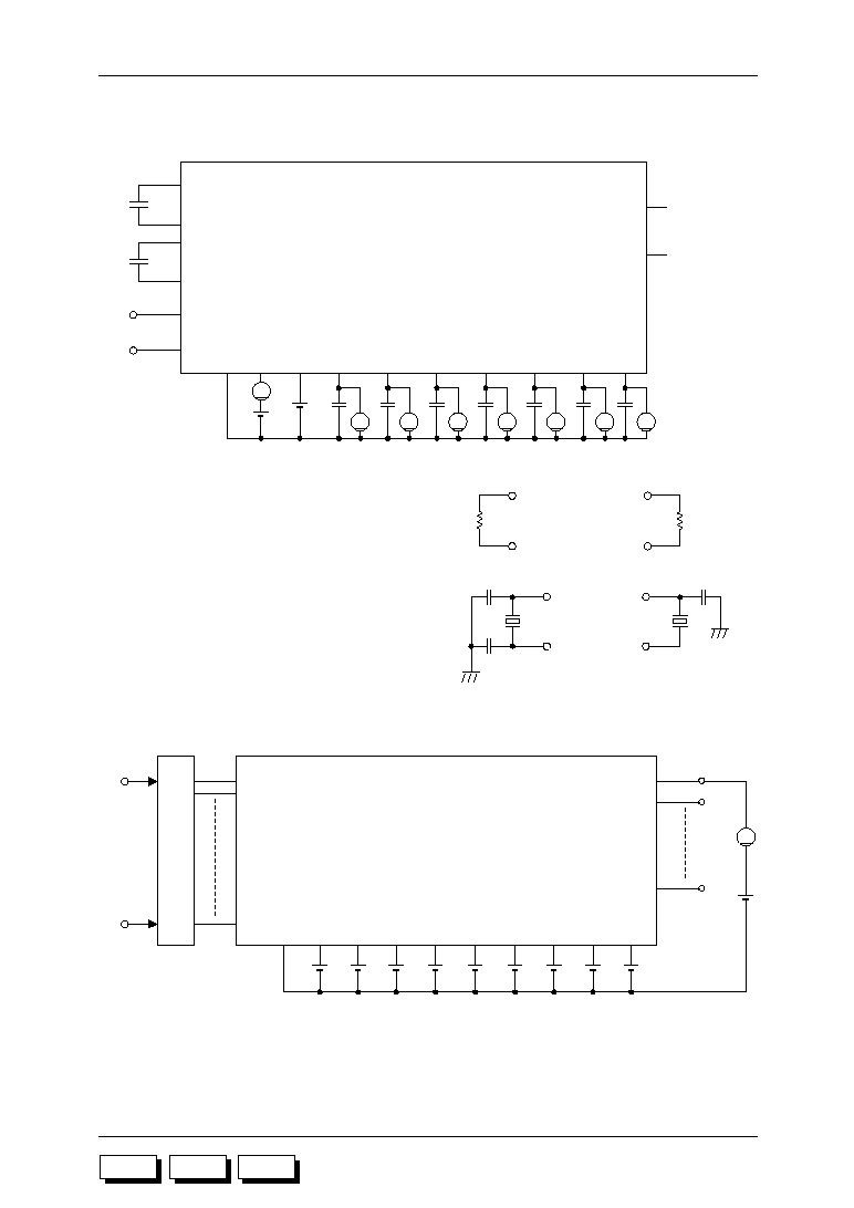
Appendix-30
ML63187/189B/193 User's Manual
Appendix E
M187
M189B
M193
Measuring circuit 1
Measuring circuit 2
V
SS
A
V
IH
V
IL
*3
V
DD
V
DDI
V
DD1
V
DD2
V
DD3
V
DD4
V
DD5
V
DDH
INPUT
OUTPUT
*4
V
DDL
*3 Input logic circuit to determine the specified measuring conditions.
*4 Measured at the specified output pins.
C
b12
CB1
CB2
C
12
C1
C2
OSC0
q
OSC1
w
*1
V
SS
A
V
DD
V
DDI
V
DD1
V
C
a
V
DD2
V
C
b
V
DD3
V
C
c
V
DD4
V
C
d
V
DD5
V
C
e
V
DDH
V
C
h
XT0
XT1
C
a
, C
b
, C
c
, C
d
, C
e
, C
l
, C
12
C
b12
, C
h
C
G
C
L0
C
L1
Ceramic Resonator
: 0.1
mF
: 1
mF
: 15 pF
: 30 pF
: 30 pF
: CSA2.00MG (2 MHz)
CSB1000J (1 MHz)
(Murata MFG.-make)
C
L0
C
L1
q
w
q
w
*1 RC Oscillator
R
OSH
Ceramic Oscillator
Ceramic
Resonator
V
DDL
V
C
l
*2
e
r
C
G
e
r
e
r
*2 RC Oscillator
R
OSL
Crystal Oscillator
32.768 kHz
Crystal

Appendix-31
ML63187/189B/193 User's Manual
Appendix E
M187
M189B
M193
Measuring circuit 3
V
SS
V
DD
V
DDI
V
DD1
V
DD2
V
DD3
V
DD4
V
DD5
V
DDH
INPUT
OUTPUT
A
*5
V
DDL
Measuring circuit 4
V
SS
V
IH
V
IL
*5
V
DD
V
DDI
V
DD1
V
DD2
V
DD3
V
DD4
V
DD5
V
DDH
INPUT
OUTPUT
*5 Measured at the specified input pins.
Waveform
Monitoring
V
DDL
Appendix-32
ML63187/189B/193 User's Manual
Appendix E
M187
M189B
M193
AC Characteristics (Serial Interface, Serial Port)
[Only applies to the ML63193]
(V
DD
= 0.9 to 5.5 V, V
DDH
= 1.8 to 5.5 V, V
SS
= 0 V, V
DDI
= 5.0 V, Ta = ≠20 to +70
∞
C unless
otherwise specified)
(1) Synchronous Communication
Synchronous Communication Timing Waveforms
("H" level = 4.0 V, "L" level = 1.0 V)
Parameter
Symbol
Condition
Unit
--
TXC/RXC Input Fall Time
Max.
Typ.
Min.
t
f
--
ms
--
1.0
--
TXC/RXC Input Rise Time
t
r
--
ms
--
1.0
0.8
TXC/RXC Input "L" Level
Pulse Width
t
CWL
--
ms
--
--
0.8
TXC/RXC Input "H" Level
Pulse Width
t
CWH
--
ms
--
--
2.0
TXC/RXC Input Cycle Time
t
CYC
--
ms
--
--
--
TXC/RXC Output Cycle Time
t
CYC(O)
CPU in operation state at 32.768 kHz
ms
30.5
--
--
TXD Output Delay Time
t
DDR
Output load capacitance 10 pF
ms
--
0.4
0.5
RXD Input Setup Time
t
DS
--
ms
--
--
0.8
RXD Input Hold Time
t
DH
--
ms
--
--
TXD (PC.3)
RXD (PC.0)
t
CYC
t
DDR
t
r
t
f
t
CWH
t
CWL
t
DDR
t
DS
t
DS
t
DH
V
DDI
V
SS
V
DDI
V
SS
V
DDI
V
SS
TXC (PC.1)/RXC (PC.2)
M193
Appendix-33
ML63187/189B/193 User's Manual
Appendix E
M187
M189B
M193
(2) UART Communication
Parameter
Symbol
Condition
Unit
T
BRT
≠T
CR
Transmit Baud Rate
Max.
Typ.
Min.
T
BRT
T
BRT
=1/f
BRT
T
CR
=1/f
OSC
s
T
BRT
T
BRT
+T
CR
R
BRT
•0.97
Receive Baud Rate
R
BRT
s
R
BRT
R
BRT
•1.03
R
BRT
=1/f
BRT
f
BRT
: Baud rates (1200, 2400, 4800, 9600 bps)
UART Communication Timing Waveforms
("H" level = 4.0 V, "L" level = 1.0 V)
TXD (PC.3)
T
BRT
V
DDI
V
SS
RXD (PC.0)
R
BRT
V
DDI
V
SS
Appendix-34
ML63187/189B/193 User's Manual
Appendix E
M187
M189B
M193
AC Characteristics (Serial Interface, Shift Register)
(V
DD
= 0.9 to 5.5 V, V
DDH
= 1.8 to 5.5 V, V
SS
= 0 V, V
DDI
= 5.0 V, Ta = ≠20 to +70
∞
C unless
otherwise specified)
AC characteristics timing
("H" level = 4.0 V, "L" level = 1.0 V)
Parameter
Symbol
Condition
Unit
--
SCLK Input Fall Time
Max.
Typ.
Min.
t
f
--
ms
--
1.0
--
SCLK Input Rise Time
t
r
--
ms
--
1.0
0.8
SCLK Input "L" Level
Pulse Width
t
CWL
--
ms
--
--
0.8
SCLK Input "H" Level
Pulse Width
t
CWH
--
ms
--
--
1.8
SCLK Input Cycle Time
t
CYC
V
DDI
= 5 V to V
DD
ms
--
--
--
SCLK Output Cycle Time
t
CYC1(O)
CPU in operation state at 32.768 kHz
ms
30.5
--
--
t
CYC2(O)
CPU in operation at 2 MHz
V
DD
= V
DDH
= 1.8 V to 3.5 V
ms
0.5
--
--
SOUT Output Delay Time
t
DDR
C
l
= 10 pF
ms
--
0.4
0.5
SIN Input Setup Time
t
DS
--
ms
--
--
0.8
SIN Input Hold Time
t
DH
--
ms
--
--
SOUT (PE.1)
SIN (PE.0)
t
CYC
t
DDR
t
r
t
f
t
CWH
t
CWL
t
DDR
t
DS
t
DS
t
DH
V
DDI
V
SS
V
DDI
V
SS
V
DDI
V
SS
SCLK (PE.2)

Appendix-35
ML63187/189B/193 User's Manual
Appendix F
M187
M189B
M193
Appendix F Instruction List
The format used in the list of instructions is indicated below.
INSTRUCTION CODE
FLAG
MNEMONIC
OPERATION
W C
15 14 13 12 11 10 9 8 7 6 5 4 3 2 1 0 Z C G
Flags marked with (
˜) are
affected by instruction
execution, and those that
are not affected with a dash.
Indicates the instruction code content.
For a 2-word long instruction, the first
row shows the first word, and the
second row the second word.
Indicates the number of machine
cycles needed to execute the
instruction.
Indicates the instruction word
length.
Indicates the instruction
function.
Indicates the short-form name
for the instruction.

Appendix-36
ML63187/189B/193 User's Manual
Appendix F
M187
M189B
M193
Transfer Instructions
15
1
MOV direct,A
INSTRUCTION CODE
FLAG
MNEMONIC
OPERATION
W C
14 13 12 11 10 9 8 7 6 5 4 3 2 1 0 Z C G
direct
®A
1 1
1 0 0 r
11
r
10
r
9
r
8
r
7
r
6
r
5
r
4
r
3
r
2
r
1
r
0
-- -- --
0
MOV [HL],A
[HL]
®A
1 1
0 0 0 0 1
0 0 0 0 1 0 0 0 0 0 -- -- --
0
MOV [XY],A
[XY]
®A
1 1
0 0 0 0 1
0 0 0 0 1 1 0 0 0 0 -- -- --
0
MOV E:[HL],A
E:[HL]
®A
1 1
0 0 0 0 1
0 0 0 0 0 0 0 0 0 0 -- -- --
0
MOV E:[XY],A
E:[XY]
®A
1 1
0 0 0 0 1
0 0 0 0 0 1 0 0 0 0 -- -- --
0
MOV [HL+],A
[HL]
®A,HL®HL+1
1 1
0 0 0 0 1
0 0 0 0 1 0 1 0 0 0 -- --
˜
0
MOV [XY+],A
[XY]
®A,XY®XY+1
1 1
0 0 0 0 1
0 0 0 0 1 1 1 0 0 0 -- --
˜
0
MOV E:[HL+],A E:[HL]
®A,HL®HL+1
1 1
0 0 0 0 1
0 0 0 0 0 0 1 0 0 0 -- --
˜
0
MOV E:[XY+],A E:[XY]
®A,XY®XY+1
1 1
0 0 0 0 1
0 0 0 0 0 1 1 0 0 0 -- --
˜
0
MOV •cur,#i4
cur,A
®i4
1 1
1 0 0 i
3
i
2
i
1
i
0
r
7
r
6
r
5
r
4
r
3
r
2
r
1
r
0
˜ -- --
0
MOV [HL],#i4
[HL],A
®i4
1 1
0 0 0 0 1
1 0 0 1 1 0 i
3
i
2
i
1
i
0
˜ -- --
0
MOV [XY],#i4
[XY],A
®i4
1 1
0 0 0 0 1
1 0 0 1 1 1 i
3
i
2
i
1
i
0
˜ -- --
0
MOV E:[HL],#i4 E:[HL],A
®i4
1 1
0 0 0 0 1
1 0 0 1 0 0 i
3
i
2
i
1
i
0
˜ -- --
0
MOV E:[XY],#i4 E:[XY],A
®i4
1 1
0 0 0 0 1
1 0 0 1 0 1 i
3
i
2
i
1
i
0
˜ -- --
0
MOV [HL+],#i4
[HL],A
®i4,HL®HL+1
1 1
0 0 0 0 1
1 1 0 1 1 0 i
3
i
2
i
1
i
0
˜ -- ˜
0
MOV [XY+],#i4
[XY],A
®i4,XY®XY+1
1 1
0 0 0 0 1
1 1 0 1 1 1 i
3
i
2
i
1
i
0
˜ -- ˜
0
MOV E:[HL+],#i4 E:[HL],A
®i4,HL®HL+1 1 1
0 0 0 0 1
1 1 0 1 0 0 i
3
i
2
i
1
i
0
˜ -- ˜
0
MOV E:[XY+],#i4 E:[XY],A
®i4,XY®XY+1 1 1
0 0 0 0 1
1 1 0 1 0 1 i
3
i
2
i
1
i
0
˜ -- ˜
0
MOV A,#i4
A
®i4
1 1
0 0 0 0 0
0 1 1 1 0 0 i
3
i
2
i
1
i
0
˜ -- --
1
MOV A,direct
A
®direct
1 1
1 0 1 r
11
r
10
r
9
r
8
r
7
r
6
r
5
r
4
r
3
r
2
r
1
r
0
˜ -- --
0
MOV A,[HL]
A
®[HL]
1 1
0 0 0 0 0
1 1 0 0 1 0 0 0 0 0
˜ -- --
0
MOV A,[XY]
A
®[XY]
1 1
0 0 0 0 0
1 1 0 0 1 1 0 0 0 0
˜ -- --
0
MOV A,E:[HL]
A
®E:[HL]
1 1
0 0 0 0 0
1 1 0 0 0 0 0 0 0 0
˜ -- --
0
MOV A,E:[XY]
A
®E:[XY]
1 1
0 0 0 0 0
1 1 0 0 0 1 0 0 0 0
˜ -- --
0
MOV A,[HL+]
A
®[HL],HL®HL+1
1 1
0 0 0 0 0
1 1 0 0 1 0 1 0 0 0
˜ -- ˜
0
MOV A,[XY+]
A
®[XY],XY®XY+1
1 1
0 0 0 0 0
1 1 0 0 1 1 1 0 0 0
˜ -- ˜
0
MOV A,E:[HL+] A
®E:[HL],HL®HL+1
1 1
0 0 0 0 0
1 1 0 0 0 0 1 0 0 0
˜ -- ˜
0
MOV A,E:[XY+] A
®E:[XY],XY®XY+1
1 1
0 0 0 0 0
1 1 0 0 0 1 1 0 0 0
˜ -- ˜
0
XCH A,sfr
A
¥sfr
1 1
0 1 0 1 1
1 0 r
7
r
6
r
5
r
4
r
3
r
2
r
1
r
0
-- -- --
0
XCH A,•cur
A
¥cur
1 1
0 1 1 1 1
1 0 r
7
r
6
r
5
r
4
r
3
r
2
r
1
r
0
-- -- --
0
XCH A,[HL]
A
¥[HL]
1 1
0 0 0 0 0
1 1 0 0 1 0 0 0 0 1 -- -- --
0
XCH A,[XY]
A
¥[XY]
1 1
0 0 0 0 0
1 1 0 0 1 1 0 0 0 1 -- -- --
0
XCH A,E:[HL]
A
¥E:[HL]
1 1
0 0 0 0 0
1 1 0 0 0 0 0 0 0 1 -- -- --
0
XCH A,E:[XY]
A
¥E:[XY]
1 1
0 0 0 0 0
1 1 0 0 0 1 0 0 0 1 -- -- --
0
XCH A,[HL+]
A
¥[HL],HL®HL+1
1 1
0 0 0 0 0
1 1 0 0 1 0 1 0 0 1 -- --
˜
0
XCH A,[XY+]
A
¥[XY],XY®XY+1
1 1
0 0 0 0 0
1 1 0 0 1 1 1 0 0 1 -- --
˜
0
XCH A,E:[HL+]
A
¥E:[HL],HL®HL+1
1 1
0 0 0 0 0
1 1 0 0 0 0 1 0 0 1 -- --
˜
0
XCH A,E:[XY+]
A
¥E:[XY],XY®XY+1
1 1
0 0 0 0 0
1 1 0 0 0 1 1 0 0 1 -- --
˜

Appendix-37
ML63187/189B/193 User's Manual
Appendix F
M187
M189B
M193
Rotate Instructions
15
0
ROL sfr
INSTRUCTION CODE
FLAG
MNEMONIC
OPERATION
W C
14 13 12 11 10 9 8 7 6 5 4 3 2 1 0 Z C G
C
®{
3
sfr
0
}
®C,A®sfr
1 1
0 1 0 0 0
1 0 r
7
r
6
r
5
r
4
r
3
r
2
r
1
r
0
˜ ˜ --
0
ROL •cur
C
®{
3
cur
0
}
®C,A®cur
1 1
0 1 1 0 0
1 0 r
7
r
6
r
5
r
4
r
3
r
2
r
1
r
0
˜ ˜ --
0
ROL [HL]
C
®{
3
[HL]
0
}
®C,A®[HL] 1 1
0 0 0 0 1
0 0 0 0 1 0 0 1 1 0
˜ ˜ --
0
ROL [XY]
C
®{
3
[XY]
0
}
®C,A®[XY] 1 1
0 0 0 0 1
0 0 0 0 1 1 0 1 1 0
˜ ˜ --
0
ROL E:[HL]
C
®{
3
E:[HL]
0
}
®C,A®E:[HL] 1 1
0 0 0 0 1
0 0 0 0 0 0 0 1 1 0
˜ ˜ --
0
ROL E:[XY]
C
®{
3
E:[XY]
0
}
®C,A®E:[XY] 1 1
0 0 0 0 1
0 0 0 0 0 1 0 1 1 0
˜ ˜ --
0
ROL [HL+]
C
®{
3
[HL]
0
}
®C,A®[HL],
HL
®HL+1
1 1
0 0 0 0 1
0 0 0 0 1 0 1 1 1 0
˜ ˜ ˜
0
ROL [XY+]
C
®{
3
[XY]
0
}
®C,A®[XY],
XY
®XY+1
1 1
0 0 0 0 1
0 0 0 0 1 1 1 1 1 0
˜ ˜ ˜
0
ROL E:[HL+]
C
®{
3
E:[HL]
0
}
®C,
A
®E:[HL],HL®HL+1
1 1
0 0 0 0 1
0 0 0 0 0 0 1 1 1 0
˜ ˜ ˜
0
ROL E:[XY+]
C
®{
3
E:[XY]
0
}
®C,
A
®E:[XY],XY®XY+1
1 1
0 0 0 0 1
0 0 0 0 0 1 1 1 1 0
˜ ˜ ˜
0
ROR sfr
C
∆{
3
sfr
0
}
∆C,A®sfr
1 1
0 1 0 0 0
1 1 r
7
r
6
r
5
r
4
r
3
r
2
r
1
r
0
˜ ˜ --
0
ROR •cur
C
∆{
3
cur
0
}
∆C,A®cur
1 1
0 1 1 0 0
1 1 r
7
r
6
r
5
r
4
r
3
r
2
r
1
r
0
˜ ˜ --
0
ROR [HL]
C
∆{
3
[HL]
0
}
∆C,A®[HL] 1 1
0 0 0 0 1
0 0 0 0 1 0 0 1 1 1
˜ ˜ --
0
ROR [XY]
C
∆{
3
[XY]
0
}
∆C,A®[XY] 1 1
0 0 0 0 1
0 0 0 0 1 1 0 1 1 1
˜ ˜ --
0
ROR E:[HL]
C
∆{
3
E:[HL]
0
}
∆C,A®E:[HL] 1 1
0 0 0 0 1
0 0 0 0 0 0 0 1 1 1
˜ ˜ --
0
ROR E:[XY]
C
∆{
3
E:[XY]
0
}
∆C,A®E:[XY] 1 1
0 0 0 0 1
0 0 0 0 0 1 0 1 1 1
˜ ˜ --
0
ROR [HL+]
C
∆{
3
[HL]
0
}
∆C,A®[HL],
HL
®HL+1
1 1
0 0 0 0 1
0 0 0 0 1 0 1 1 1 1
˜ ˜ ˜
0
ROR [XY+]
C
∆{
3
[XY]
0
}
∆C,A®[XY],
XY
®XY+1
1 1
0 0 0 0 1
0 0 0 0 1 1 1 1 1 1
˜ ˜ ˜
0
ROR E:[HL+]
C
∆{
3
E:[HL]
0
}
∆C,
A
®E:[HL],HL®HL+1
1 1
0 0 0 0 1
0 0 0 0 0 0 1 1 1 1
˜ ˜ ˜
0
ROR E:[XY+]
C
∆{
3
E:[XY]
0
}
∆C,
A
®E:[XY],XY®XY+1
1 1
0 0 0 0 1
0 0 0 0 0 1 1 1 1 1
˜ ˜ ˜
Appendix-38
ML63187/189B/193 User's Manual
Appendix F
M187
M189B
M193
Increment/Decrement Instructions
15
0
INC sfr
INSTRUCTION CODE
FLAG
MNEMONIC
OPERATION
W C
14 13 12 11 10 9 8 7 6 5 4 3 2 1 0 Z C G
sfr,A
®sfr+1
1 1
0 1 0 0 0
0 0 r
7
r
6
r
5
r
4
r
3
r
2
r
1
r
0
˜ ˜ --
0
INC •cur
cur,A
®cur+1
1 1
0 1 1 0 0
0 0 r
7
r
6
r
5
r
4
r
3
r
2
r
1
r
0
˜ ˜ --
0
INC [HL]
[HL],A
®[HL]+1
1 1
0 0 0 0 1
0 1 0 0 1 0 0 0 0 0
˜ ˜ --
0
INC [XY]
[XY],A
®[XY]+1
1 1
0 0 0 0 1
0 1 0 0 1 1 0 0 0 0
˜ ˜ --
0
INC E:[HL]
E:[HL],A
®E:[HL]+1
1 1
0 0 0 0 1
0 1 0 0 0 0 0 0 0 0
˜ ˜ --
0
INC E:[XY]
E:[XY],A
®E:[XY]+1
1 1
0 0 0 0 1
0 1 0 0 0 1 0 0 0 0
˜ ˜ --
0
INC [HL+]
[HL],A
®[HL]+1,
HL
®HL+1
1 1
0 0 0 0 1
0 1 0 0 1 0 1 0 0 0
˜ ˜ ˜
0
INC [XY+]
[XY],A
®[XY]+1,
XY
®XY+1
1 1
0 0 0 0 1
0 1 0 0 1 1 1 0 0 0
˜ ˜ ˜
0
INC E:[HL+]
E:[HL],A
®E:[HL]+1,
HL
®HL+1
1 1
0 0 0 0 1
0 1 0 0 0 0 1 0 0 0
˜ ˜ ˜
0
INC E:[XY+]
E:[XY],A
®E:[XY]+1,
XY
®XY+1
1 1
0 0 0 0 1
0 1 0 0 0 1 1 0 0 0
˜ ˜ ˜
0
DEC sfr
sfr,A
®sfr≠1
1 1
0 1 0 0 0
0 1 r
7
r
6
r
5
r
4
r
3
r
2
r
1
r
0
˜ ˜ --
0
DEC •cur
cur,A
®cur≠1
1 1
0 1 1 0 0
0 1 r
7
r
6
r
5
r
4
r
3
r
2
r
1
r
0
˜ ˜ --
0
DEC [HL]
[HL],A
®[HL]≠1
1 1
0 0 0 0 1
0 1 0 0 1 0 0 0 0 1
˜ ˜ --
0
DEC [XY]
[XY],A
®[XY]≠1
1 1
0 0 0 0 1
0 1 0 0 1 1 0 0 0 1
˜ ˜ --
0
DEC E:[HL]
E:[HL],A
®E:[HL]≠1
1 1
0 0 0 0 1
0 1 0 0 0 0 0 0 0 1
˜ ˜ --
0
DEC E:[XY]
E:[XY],A
®E:[XY]≠1
1 1
0 0 0 0 1
0 1 0 0 0 1 0 0 0 1
˜ ˜ --
0
DEC [HL+]
[HL],A
®[HL]≠1,
HL
®HL+1
1 1
0 0 0 0 1
0 1 0 0 1 0 1 0 0 1
˜ ˜ ˜
0
DEC [XY+]
[XY],A
®[XY]≠1,
XY
®XY+1
1 1
0 0 0 0 1
0 1 0 0 1 1 1 0 0 1
˜ ˜ ˜
0
DEC E:[HL+]
E:[HL],A
®E:[HL]≠1,
HL
®HL+1
1 1
0 0 0 0 1
0 1 0 0 0 0 1 0 0 1
˜ ˜ ˜
0
DEC E:[XY+]
E:[XY],A
®E:[XY]≠1,
XY
®XY+1
1 1
0 0 0 0 1
0 1 0 0 0 1 1 0 0 1
˜ ˜ ˜

Appendix-39
ML63187/189B/193 User's Manual
Appendix F
M187
M189B
M193
Arithmetic Instructions
15
0
ADD sfr,A
INSTRUCTION CODE
FLAG
MNEMONIC
OPERATION
W C
14 13 12 11 10 9 8 7 6 5 4 3 2 1 0 Z C G
sfr,A
®sfr+A
1 1
0 1 0 0 1
0 0 r
7
r
6
r
5
r
4
r
3
r
2
r
1
r
0
˜ ˜ --
0
ADD •cur,A
cur,A
®cur+A
1 1
0 1 1 0 1
0 0 r
7
r
6
r
5
r
4
r
3
r
2
r
1
r
0
˜ ˜ --
0
ADD [HL],A
[HL],A
®[HL]+A
1 1
0 0 0 0 1
0 1 0 0 1 0 0 0 1 0
˜ ˜ --
0
ADD [XY],A
[XY],A
®[XY]+A
1 1
0 0 0 0 1
0 1 0 0 1 1 0 0 1 0
˜ ˜ --
0
ADD E:[HL],A
E:[HL],A
®E:[HL]+A
1 1
0 0 0 0 1
0 1 0 0 0 0 0 0 1 0
˜ ˜ --
0
ADD E:[XY],A
E:[XY],A
®E:[XY]+A
1 1
0 0 0 0 1
0 1 0 0 0 1 0 0 1 0
˜ ˜ --
0
ADD [HL+],A
[HL],A
®[HL]+A,
HL
®HL+1
1 1
0 0 0 0 1
0 1 0 0 1 0 1 0 1 0
˜ ˜ ˜
0
ADD [XY+],A
[XY],A
®[XY]+A,
XY
®XY+1
1 1
0 0 0 0 1
0 1 0 0 1 1 1 0 1 0
˜ ˜ ˜
0
ADD E:[HL+],A
E:[HL],A
®E:[HL]+A,
HL
®HL+1
1 1
0 0 0 0 1
0 1 0 0 0 0 1 0 1 0
˜ ˜ ˜
0
ADD E:[XY+],A
E:[XY],A
®E:[XY]+A,
XY
®XY+1
1 1
0 0 0 0 1
0 1 0 0 0 1 1 0 1 0
˜ ˜ ˜
1
ADD •cur,#i4
cur,A
®cur+i4
1 1
0 0 0 i
3
i
2
i
1
i
0
r
7
r
6
r
5
r
4
r
3
r
2
r
1
r
0
˜ ˜ --
0
ADD [HL],#i4
[HL],A
®[HL]+i4
1 1
0 0 0 0 0
0 0 1 0 1 0 i
3
i
2
i
1
i
0
˜ ˜ --
0
ADD [XY],#i4
[XY],A
®[XY]+i4
1 1
0 0 0 0 0
0 0 1 0 1 1 i
3
i
2
i
1
i
0
˜ ˜ --
0
ADD E:[HL],#i4 E:[HL],A
®E:[HL]+i4
1 1
0 0 0 0 0
0 0 1 0 0 0 i
3
i
2
i
1
i
0
˜ ˜ --
0
ADD E:[XY],#i4 E:[XY],A
®E:[XY]+i4
1 1
0 0 0 0 0
0 0 1 0 0 1 i
3
i
2
i
1
i
0
˜ ˜ --
0
ADD [HL+],#i4
[HL],A
®[HL]+i4,
HL
®HL+1
1 1
0 0 0 0 0
0 1 1 0 1 0 i
3
i
2
i
1
i
0
˜ ˜ ˜
0
ADD [XY+],#i4
[XY],A
®[XY]+i4,
XY
®XY+1
1 1
0 0 0 0 0
0 1 1 0 1 1 i
3
i
2
i
1
i
0
˜ ˜ ˜
0
ADD E:[HL+],#i4
E:[HL],A
®E:[HL]+i4,
HL
®HL+1
1 1
0 0 0 0 0
0 1 1 0 0 0 i
3
i
2
i
1
i
0
˜ ˜ ˜
0
ADD E:[XY+],#i4
E:[XY],A
®E:[XY]+i4,
XY
®XY+1
1 1
0 0 0 0 0
0 1 1 0 0 1 i
3
i
2
i
1
i
0
˜ ˜ ˜
0
ADC sfr,A
sfr,A
®sfr+A+C
1 1
0 1 0 0 1
0 1 r
7
r
6
r
5
r
4
r
3
r
2
r
1
r
0
˜ ˜ --
0
ADC •cur,A
cur,A
®cur+A+C
1 1
0 1 1 0 1
0 1 r
7
r
6
r
5
r
4
r
3
r
2
r
1
r
0
˜ ˜ --
0
ADC [HL],A
[HL],A
®[HL]+A+C
1 1
0 0 0 0 1
0 1 0 0 1 0 0 0 1 1
˜ ˜ --
0
ADC [XY],A
[XY],A
®[XY]+A+C
1 1
0 0 0 0 1
0 1 0 0 1 1 0 0 1 1
˜ ˜ --
0
ADC E:[HL],A
E:[HL],A
®E:[HL]+A+C
1 1
0 0 0 0 1
0 1 0 0 0 0 0 0 1 1
˜ ˜ --
0
ADC E:[XY],A
E:[XY],A
®E:[XY]+A+C
1 1
0 0 0 0 1
0 1 0 0 0 1 0 0 1 1
˜ ˜ --
0
ADC [HL+],A
[HL],A
®[HL]+A+C,
HL
®HL+1
1 1
0 0 0 0 1
0 1 0 0 1 0 1 0 1 1
˜ ˜ ˜
0
ADC [XY+],A
[XY],A
®[XY]+A+C,
XY
®XY+1
1 1
0 0 0 0 1
0 1 0 0 1 1 1 0 1 1
˜ ˜ ˜
0
ADC E:[HL+],A
E:[HL],A
®E:[HL]+A+C,
HL
®HL+1
1 1
0 0 0 0 1
0 1 0 0 0 0 1 0 1 1
˜ ˜ ˜
0
ADC E:[XY+],A
E:[XY],A
®E:[XY]+A+C,
XY
®XY+1
1 1
0 0 0 0 1
0 1 0 0 0 1 1 0 1 1
˜ ˜ ˜
Appendix-40
ML63187/189B/193 User's Manual
Appendix F
M187
M189B
M193
Arithmetic Instructions (continued)
15
0
ADCD sfr,A
INSTRUCTION CODE
FLAG
MNEMONIC
OPERATION
W C
14 13 12 11 10 9 8 7 6 5 4 3 2 1 0 Z C G
sfr,A
®decimal adjustment
{sfr+A+C}
1 1
0 1 0 0 1
1 0 r
7
r
6
r
5
r
4
r
3
r
2
r
1
r
0
˜ ˜ --
0
ADCD •cur,A
cur,A
®decimal adjustment
{cur+A+C}
1 1
0 1 1 0 1
1 0 r
7
r
6
r
5
r
4
r
3
r
2
r
1
r
0
˜ ˜ --
0
ADCD [HL],A
[HL],A
®decimal adjustment
{[HL]+A+C}
1 1
0 0 0 0 1
0 1 0 0 1 0 0 1 0 0
˜ ˜ --
0
ADCD [XY],A
[XY],A
®decimal adjustment
{[XY]+A+C}
1 1
0 0 0 0 1
0 1 0 0 1 1 0 1 0 0
˜ ˜ --
0
ADCD E:[HL],A
E:[HL],A
®decimal
adjustment {E:[HL]+A+C}
1 1
0 0 0 0 1
0 1 0 0 0 0 0 1 0 0
˜ ˜ --
0
ADCD E:[XY],A
E:[XY],A
®decimal
adjustment {E:[XY]+A+C}
1 1
0 0 0 0 1
0 1 0 0 0 1 0 1 0 0
˜ ˜ --
0
ADCD [HL+],A
[HL],A
®decimal
adjustment {[HL]+A+C},
HL
®HL+1
1 1
0 0 0 0 1
0 1 0 0 1 0 1 1 0 0
˜ ˜ ˜
0
ADCD [XY+],A
[XY],A
®decimal
adjustment {[XY]+A+C},
XY
®XY+1
1 1
0 0 0 0 1
0 1 0 0 1 1 1 1 0 0
˜ ˜ ˜
0
ADCD E:[HL+],A
E:[HL],A
®decimal
adjustment {E:[HL]+A+C},
HL
®HL+1
1 1
0 0 0 0 1
0 1 0 0 0 0 1 1 0 0
˜ ˜ ˜
0
ADCD E:[XY+],A
E:[XY],A
®decimal
adjustment {E:[XY]+A+C},
XY
®XY+1
1 1
0 0 0 0 1
0 1 0 0 0 1 1 1 0 0
˜ ˜ ˜
0
ADCJ •cur,n
cur,A
®n-ary adjustment
{cur+C}
1 1
0 0 1 0 n
2
n
1
n
0
r
7
r
6
r
5
r
4
r
3
r
2
r
1
r
0
˜ ˜ --
0
ADCJ [HL],n
[HL],A
®n-ary adjustment
{[HL]+C}
1 1
0 0 0 0 1
1 0 0 0 1 0 0 n
2
n
1
n
0
˜ ˜ --
0
ADCJ [XY],n
[XY],A
®n-ary adjustment
{[XY]+C}
1 1
0 0 0 0 1
1 0 0 0 1 1 0 n
2
n
1
n
0
˜ ˜ --
0
ADCJ E:[HL],n
E:[HL],A
®n-ary adjustment
{E:[HL]+C}
1 1
0 0 0 0 1
1 0 0 0 0 0 0 n
2
n
1
n
0
˜ ˜ --
0
ADCJ E:[XY],n
E:[XY],A
®n-ary adjustment
{E:[XY]+C}
1 1
0 0 0 0 1
1 0 0 0 0 1 0 n
2
n
1
n
0
˜ ˜ --
0
ADCJ [HL+],n
[HL],A
®n-ary adjustment
{[HL]+C},HL
®HL+1
1 1
0 0 0 0 1
1 1 0 0 1 0 0 n
2
n
1
n
0
˜ ˜ ˜
0
ADCJ [XY+],n
[XY],A
®n-ary adjustment
{[XY]+C},XY
®XY+1
1 1
0 0 0 0 1
1 1 0 0 1 1 0 n
2
n
1
n
0
˜ ˜ ˜
0
ADCJ E:[HL+],n
E:[HL],A
®n-ary adjustment
{E:[HL]+C},HL
®HL+1
1 1
0 0 0 0 1
1 1 0 0 0 0 0 n
2
n
1
n
0
˜ ˜ ˜
0
ADCJ E:[XY+],n
E:[XY],A
®n-ary adjustment
{E:[XY]+C},XY
®XY+1
1 1
0 0 0 0 1
1 1 0 0 0 1 0 n
2
n
1
n
0
˜ ˜ ˜
Appendix-41
ML63187/189B/193 User's Manual
Appendix F
M187
M189B
M193
Arithmetic Instructions (continued)
15
0
SUB sfr,A
INSTRUCTION CODE
FLAG
MNEMONIC
OPERATION
W C
14 13 12 11 10 9 8 7 6 5 4 3 2 1 0 Z C G
sfr,A
®sfr≠A
1 1
0 1 0 0 1
1 1 r
7
r
6
r
5
r
4
r
3
r
2
r
1
r
0
˜ ˜ --
0
SUB •cur,A
cur,A
®cur≠A
1 1
0 1 1 0 1
1 1 r
7
r
6
r
5
r
4
r
3
r
2
r
1
r
0
˜ ˜ --
0
SUB [HL],A
[HL],A
®[HL]≠A
1 1
0 0 0 0 1
0 1 0 0 1 0 0 1 0 1
˜ ˜ --
0
SUB [XY],A
[XY],A
®[XY]≠A
1 1
0 0 0 0 1
0 1 0 0 1 1 0 1 0 1
˜ ˜ --
0
SUB E:[HL],A
E:[HL],A
®E:[HL]≠A
1 1
0 0 0 0 1
0 1 0 0 0 0 0 1 0 1
˜ ˜ --
0
SUB E:[XY],A
E:[XY],A
®E:[XY]≠A
1 1
0 0 0 0 1
0 1 0 0 0 1 0 1 0 1
˜ ˜ --
0
SUB [HL+],A
[HL],A
®[HL]≠A,
HL
®HL+1
1 1
0 0 0 0 1
0 1 0 0 1 0 1 1 0 1
˜ ˜ ˜
0
SUB [XY+],A
[XY],A
®[XY]≠A,
XY
®XY+1
1 1
0 0 0 0 1
0 1 0 0 1 1 1 1 0 1
˜ ˜ ˜
0
SUB E:[HL+],A
E:[HL],A
®E:[HL]≠A,
HL
®HL+1
1 1
0 0 0 0 1
0 1 0 0 0 0 1 1 0 1
˜ ˜ ˜
0
SUB E:[XY+],A
E:[XY],A
®E:[XY]≠A,
XY
®XY+1
1 1
0 0 0 0 1
0 1 0 0 0 1 1 1 0 1
˜ ˜ ˜
1
SUB •cur,#i4
cur,A
®cur≠i4
1 1
0 0 1 i
3
i
2
i
1
i
0
r
7
r
6
r
5
r
4
r
3
r
2
r
1
r
0
˜ ˜ --
0
SUB [HL],#i4
[HL],A
®[HL]≠i4
1 1
0 0 0 0 0
1 0 1 0 1 0 i
3
i
2
i
1
i
0
˜ ˜ --
0
SUB [XY],#i4
[XY],A
®[XY]≠i4
1 1
0 0 0 0 0
1 0 1 0 1 1 i
3
i
2
i
1
i
0
˜ ˜ --
0
SUB E:[HL],#i4
E:[HL],A
®E:[HL]≠i4
1 1
0 0 0 0 0
1 0 1 0 0 0 i
3
i
2
i
1
i
0
˜ ˜ --
0
SUB E:[XY],#i4
E:[XY],A
®E:[XY]≠i4
1 1
0 0 0 0 0
1 0 1 0 0 1 i
3
i
2
i
1
i
0
˜ ˜ --
0
SUB [HL+],#i4
[HL],A
®[HL]≠i4,
HL
®HL+1
1 1
0 0 0 0 0
1 1 1 0 1 0 i
3
i
2
i
1
i
0
˜ ˜ ˜
0
SUB [XY+],#i4
[XY],A
®[XY]≠i4,
XY
®XY+1
1 1
0 0 0 0 0
1 1 1 0 1 1 i
3
i
2
i
1
i
0
˜ ˜ ˜
0
SUB E:[HL+],#i4
E:[HL],A
®E:[HL]≠i4,
HL
®HL+1
1 1
0 0 0 0 0
1 1 1 0 0 0 i
3
i
2
i
1
i
0
˜ ˜ ˜
0
SUB E:[XY+],#i4
E:[XY],A
®E:[XY]≠i4,
XY
®XY+1
1 1
0 0 0 0 0
1 1 1 0 0 1 i
3
i
2
i
1
i
0
˜ ˜ ˜
0
SBC sfr,A
sfr,A
®sfr≠A≠C
1 1
0 1 0 1 0
0 0 r
7
r
6
r
5
r
4
r
3
r
2
r
1
r
0
˜ ˜ --
0
SBC •cur,A
cur,A
®cur≠A≠C
1 1
0 1 1 1 0
0 0 r
7
r
6
r
5
r
4
r
3
r
2
r
1
r
0
˜ ˜ --
0
SBC [HL],A
[HL],A
®[HL]≠A≠C
1 1
0 0 0 0 1
0 1 0 0 1 0 0 1 1 0
˜ ˜ --
0
SBC [XY],A
[XY],A
®[XY]≠A≠C
1 1
0 0 0 0 1
0 1 0 0 1 1 0 1 1 0
˜ ˜ --
0
SBC E:[HL],A
E:[HL],A
®E:[HL]≠A≠C
1 1
0 0 0 0 1
0 1 0 0 0 0 0 1 1 0
˜ ˜ --
0
SBC E:[XY],A
E:[XY],A
®E:[XY]≠A≠C
1 1
0 0 0 0 1
0 1 0 0 0 1 0 1 1 0
˜ ˜ --
0
SBC [HL+],A
[HL],A
®[HL]≠A≠C,
HL
®HL+1
1 1
0 0 0 0 1
0 1 0 0 1 0 1 1 1 0
˜ ˜ ˜
0
SBC [XY+],A
[XY],A
®[XY]≠A≠C,
XY
®XY+1
1 1
0 0 0 0 1
0 1 0 0 1 1 1 1 1 0
˜ ˜ ˜
0
SBC E:[HL+],A
E:[HL],A
®E:[HL]≠A≠C,
HL
®HL+1
1 1
0 0 0 0 1
0 1 0 0 0 0 1 1 1 0
˜ ˜ ˜
0
SBC E:[XY+],A
E:[XY],A
®E:[XY]≠A≠C,
XY
®XY+1
1 1
0 0 0 0 1
0 1 0 0 0 1 1 1 1 0
˜ ˜ ˜

Appendix-42
ML63187/189B/193 User's Manual
Appendix F
M187
M189B
M193
Arithmetic Instructions (continued)
15
0
SBCD sfr,A
INSTRUCTION CODE
FLAG
MNEMONIC
OPERATION
W C
14 13 12 11 10 9 8 7 6 5 4 3 2 1 0 Z C G
sfr,A
®decimal adjustment
{sfr≠A≠C}
1 1
0 1 0 1 0
0 1 r
7
r
6
r
5
r
4
r
3
r
2
r
1
r
0
˜ ˜ --
0
SBCD •cur,A
cur,A
®decimal adjustment
{cur≠A≠C}
1 1
0 1 1 1 0
0 1 r
7
r
6
r
5
r
4
r
3
r
2
r
1
r
0
˜ ˜ --
0
SBCD [HL],A
[HL],A
®decimal adjustment
{[HL]≠A≠C}
1 1
0 0 0 0 1
0 1 0 0 1 0 0 1 1 1
˜ ˜ --
0
SBCD [XY],A
[XY],A
®decimal adjustment
{[XY]≠A≠C}
1 1
0 0 0 0 1
0 1 0 0 1 1 0 1 1 1
˜ ˜ --
0
SBCD E:[HL],A
E:[HL],A
®decimal
adjustment {E:[HL]≠A≠C}
1 1
0 0 0 0 1
0 1 0 0 0 0 0 1 1 1
˜ ˜ --
0
SBCD E:[XY],A
E:[XY],A
®decimal
adjustment {E:[XY]≠A≠C}
1 1
0 0 0 0 1
0 1 0 0 0 1 0 1 1 1
˜ ˜ --
0
SBCD [HL+],A
[HL],A
®decimal
adjustment {[HL]≠A≠C},
HL
®HL+1
1 1
0 0 0 0 1
0 1 0 0 1 0 1 1 1 1
˜ ˜ ˜
0
SBCD [XY+],A
[XY],A
®decimal
adjustment {[XY]≠A≠C},
XY
®XY+1
1 1
0 0 0 0 1
0 1 0 0 1 1 1 1 1 1
˜ ˜ ˜
0
SBCD E:[HL+],A
E:[HL],A
®decimal
adjustment {E:[HL]≠A≠C},
HL
®HL+1
1 1
0 0 0 0 1
0 1 0 0 0 0 1 1 1 1
˜ ˜ ˜
0
SBCD E:[XY+],A
E:[XY],A
®decimal
adjustment {E:[XY]≠A≠C},
XY
®XY+1
1 1
0 0 0 0 1
0 1 0 0 0 1 1 1 1 1
˜ ˜ ˜
0
SBCJ •cur,n
1 1
0 0 1 1 n
2
n
1
n
0
r
7
r
6
r
5
r
4
r
3
r
2
r
1
r
0
˜ ˜ --
0
SBCJ [HL],n
1 1
0 0 0 0 1
1 0 0 0 1 0 1 n
2
n
1
n
0
˜ ˜ --
0
SBCJ [XY],n
1 1
0 0 0 0 1
1 0 0 0 1 1 1 n
2
n
1
n
0
˜ ˜ --
0
SBCJ E:[HL],n
1 1
0 0 0 0 1
1 0 0 0 0 0 1 n
2
n
1
n
0
˜ ˜ --
0
SBCJ E:[XY],n
1 1
0 0 0 0 1
1 0 0 0 0 1 1 n
2
n
1
n
0
˜ ˜ --
0
SBCJ [HL+],n
1 1
0 0 0 0 1
1 1 0 0 1 0 1 n
2
n
1
n
0
˜ ˜ ˜
0
SBCJ [XY+],n
1 1
0 0 0 0 1
1 1 0 0 1 1 1 n
2
n
1
n
0
˜ ˜ ˜
0
SBCJ E:[HL+],n
1 1
0 0 0 0 1
1 1 0 0 0 0 1 n
2
n
1
n
0
˜ ˜ ˜
0
SBCJ E:[XY+],n
1 1
0 0 0 0 1
1 1 0 0 0 1 1 n
2
n
1
n
0
˜ ˜ ˜
cur,A
®n-ary adjustment
{cur≠C}
[HL],A
®n-ary adjustment
{[HL]≠C}
[XY],A
®n-ary adjustment
{[XY]≠C}
E:[HL],A
®n-ary adjustment
{E:[HL]≠C}
E:[XY],A
®n-ary adjustment
{E:[XY]≠C}
[HL],A
®n-ary adjustment
{[HL]≠C},HL
®HL+1
[XY],A
®n-ary adjustment
{[XY]≠C},XY
®XY+1
E:[HL],A
®n-ary adjustment
{E:[HL]≠C},HL
®HL+1
E:[XY],A
®n-ary adjustment
{E:[XY]≠C},XY
®XY+1

Appendix-43
ML63187/189B/193 User's Manual
Appendix F
M187
M189B
M193
Compare Instructions
15
0
CMP sfr,A
INSTRUCTION CODE
FLAG
MNEMONIC
OPERATION
W C
14 13 12 11 10 9 8 7 6 5 4 3 2 1 0 Z C G
sfr≠A
1 1
0 1 0 1 0
1 0 r
7
r
6
r
5
r
4
r
3
r
2
r
1
r
0
˜ ˜ --
0
CMP •cur,A
cur≠A
1 1
0 1 1 1 0
1 0 r
7
r
6
r
5
r
4
r
3
r
2
r
1
r
0
˜ ˜ --
0
CMP [HL],A
[HL]≠A
1 1
0 0 0 0 1
0 0 0 0 1 0 0 1 0 0
˜ ˜ --
0
CMP [XY],A
[XY]≠A
1 1
0 0 0 0 1
0 0 0 0 1 1 0 1 0 0
˜ ˜ --
0
CMP E:[HL],A
E:[HL]≠A
1 1
0 0 0 0 1
0 0 0 0 0 0 0 1 0 0
˜ ˜ --
0
CMP E:[XY],A
E:[XY]≠A
1 1
0 0 0 0 1
0 0 0 0 0 1 0 1 0 0
˜ ˜ --
0
CMP [HL+],A
[XY]≠A,HL
®HL+1
1 1
0 0 0 0 1
0 0 0 0 1 0 1 1 0 0
˜ ˜ ˜
0
CMP [XY+],A
[XY]≠A,XY
®XY+1
1 1
0 0 0 0 1
0 0 0 0 1 1 1 1 0 0
˜ ˜ ˜
0
CMP E:[HL+],A
E:[HL]≠A,HL
®HL+1
1 1
0 0 0 0 1
0 0 0 0 0 0 1 1 0 0
˜ ˜ ˜
0
CMP E:[XY+],A
E:[XY]≠A,XY
®XY+1
1 1
0 0 0 0 1
0 0 0 0 0 1 1 1 0 0
˜ ˜ ˜
1
CMP •cur,#i4
cur≠i4
1 1
0 1 0 i
3
i
2
i
1
i
0
r
7
r
6
r
5
r
4
r
3
r
2
r
1
r
0
˜ ˜ --
0
CMP [HL],#i4
[HL]≠i4
1 1
0 0 0 0 1
1 0 1 0 1 0 i
3
i
2
i
1
i
0
˜ ˜ --
0
CMP [XY],#i4
[XY]≠i4
1 1
0 0 0 0 1
1 0 1 0 1 1 i
3
i
2
i
1
i
0
˜ ˜ --
0
CMP E:[HL],#i4 E:[HL]≠i4
1 1
0 0 0 0 1
1 0 1 0 0 0 i
3
i
2
i
1
i
0
˜ ˜ --
0
CMP E:[XY],#i4 E:[XY]≠i4
1 1
0 0 0 0 1
1 0 1 0 0 1 i
3
i
2
i
1
i
0
˜ ˜ --
0
CMP [HL+],#i4
[HL]≠i4,HL
®HL+1
1 1
0 0 0 0 1
1 1 1 0 1 0 i
3
i
2
i
1
i
0
˜ ˜ ˜
0
CMP [XY+],#i4
[XY]≠i4,XY
®XY+1
1 1
0 0 0 0 1
1 1 1 0 1 1 i
3
i
2
i
1
i
0
˜ ˜ ˜
0
CMP E:[HL+],#i4 E:[HL]≠i4,HL
®HL+1
1 1
0 0 0 0 1
1 1 1 0 0 0 i
3
i
2
i
1
i
0
˜ ˜ ˜
0
CMP E:[XY+],#i4 E:[XY]≠i4,XY
®XY+1
1 1
0 0 0 0 1
1 1 1 0 0 1 i
3
i
2
i
1
i
0
˜ ˜ ˜

Appendix-44
ML63187/189B/193 User's Manual
Appendix F
M187
M189B
M193
Logic Instructions
15
0
AND sfr,A
INSTRUCTION CODE
FLAG
MNEMONIC
OPERATION
W C
14 13 12 11 10 9 8 7 6 5 4 3 2 1 0 Z C G
sfr,A
®sfr A
1 1
0 1 0 1 0
1 1 r
7
r
6
r
5
r
4
r
3
r
2
r
1
r
0
˜ -- --
0
AND •cur,A
cur,A
®cur A
1 1
0 1 1 1 0
1 1 r
7
r
6
r
5
r
4
r
3
r
2
r
1
r
0
˜ -- --
0
AND [HL],A
[HL],A
®[HL] A
1 1
0 0 0 0 1
0 0 0 0 1 0 0 0 0 1
˜ -- --
0
AND [XY],A
[XY],A
®[XY] A
1 1
0 0 0 0 1
0 0 0 0 1 1 0 0 0 1
˜ -- --
0
AND E:[HL],A
E:[HL],A
®E:[HL] A
1 1
0 0 0 0 1
0 0 0 0 0 0 0 0 0 1
˜ -- --
0
AND E:[XY],A
E:[XY],A
®E:[XY] A
1 1
0 0 0 0 1
0 0 0 0 0 1 0 0 0 1
˜ -- --
0
AND [HL+],A
[HL],A
®[HL] A,
HL
®HL+1
1 1
0 0 0 0 1
0 0 0 0 1 0 1 0 0 1
˜ -- ˜
0
AND [XY+],A
[XY],A
®[XY] A,
XY
®XY+1
1 1
0 0 0 0 1
0 0 0 0 1 1 1 0 0 1
˜ -- ˜
0
AND E:[HL+],A
E:[HL],A
®E:[HL] A,
HL
®HL+1
1 1
0 0 0 0 1
0 0 0 0 0 0 1 0 0 1
˜ -- ˜
0
AND E:[XY+],A
E:[XY],A
®E:[XY] A,
XY
®XY+1
1 1
0 0 0 0 1
0 0 0 0 0 1 1 0 0 1
˜ -- ˜
0
AND •cur,#i4
cur,A
®cur i4
1 1
1 0 1 i
3
i
2
i
1
i
0
r
7
r
6
r
5
r
4
r
3
r
2
r
1
r
0
˜ -- --
0
AND [HL],#i4
[HL],A
®[HL] i4
1 1
0 0 0 0 1
0 0 0 1 1 0 i
3
i
2
i
1
i
0
˜ -- --
0
AND [XY],#i4
[XY],A
®[XY] i4
1 1
0 0 0 0 1
0 0 0 1 1 1 i
3
i
2
i
1
i
0
˜ -- --
0
AND E:[HL],#i4 E:[HL],A
®E:[HL] i4
1 1
0 0 0 0 1
0 0 0 1 0 0 i
3
i
2
i
1
i
0
˜ -- --
0
AND E:[XY],#i4 E:[XY],A
®E:[XY] i4
1 1
0 0 0 0 1
0 0 0 1 0 1 i
3
i
2
i
1
i
0
˜ -- --
0
AND [HL+],#i4
[HL],A
®[HL] i4,
HL
®HL+1
1 1
0 0 0 0 1
0 1 0 1 1 0 i
3
i
2
i
1
i
0
˜ -- ˜
0
AND [XY+],#i4
[XY],A
®[XY] i4,
XY
®XY+1
1 1
0 0 0 0 1
0 1 0 1 1 1 i
3
i
2
i
1
i
0
˜ -- ˜
0
AND E:[HL+],#i4
E:[HL],A
®E:[HL] i4,
HL
®HL+1
1 1
0 0 0 0 1
0 1 0 1 0 0 i
3
i
2
i
1
i
0
˜ -- ˜
0
AND E:[XY+],#i4
E:[XY],A
®E:[XY] i4,
XY
®XY+1
1 1
0 0 0 0 1
0 1 0 1 0 1 i
3
i
2
i
1
i
0
˜ -- ˜
0
OR sfr,A
sfr,A
®sfr A
1 1
0 1 0 1 1
0 0 r
7
r
6
r
5
r
4
r
3
r
2
r
1
r
0
˜ -- --
0
OR •cur,A
cur,A
®cur A
1 1
0 1 1 1 1
0 0 r
7
r
6
r
5
r
4
r
3
r
2
r
1
r
0
˜ -- --
0
OR [HL],A
[HL],A
®[HL] A
1 1
0 0 0 0 1
0 0 0 0 1 0 0 0 1 0
˜ -- --
0
OR [XY],A
[XY],A
®[XY] A
1 1
0 0 0 0 1
0 0 0 0 1 1 0 0 1 0
˜ -- --
0
OR E:[HL],A
E:[HL],A
®E:[HL] A
1 1
0 0 0 0 1
0 0 0 0 0 0 0 0 1 0
˜ -- --
0
OR E:[XY],A
E:[XY],A
®E:[XY] A
1 1
0 0 0 0 1
0 0 0 0 0 1 0 0 1 0
˜ -- --
0
OR [HL+],A
[HL],A
®[HL] A,
HL
®HL+1
1 1
0 0 0 0 1
0 0 0 0 1 0 1 0 1 0
˜ -- ˜
0
OR [XY+],A
[XY],A
®[XY] A,
XY
®XY+1
1 1
0 0 0 0 1
0 0 0 0 1 1 1 0 1 0
˜ -- ˜
0
OR E:[HL+],A
E:[HL],A
®E:[HL] A,
HL
®HL+1
1 1
0 0 0 0 1
0 0 0 0 0 0 1 0 1 0
˜ -- ˜
0
OR E:[XY+],A
E:[XY],A
®E:[XY] A,
XY
®XY+1
1 1
0 0 0 0 1
0 0 0 0 0 1 1 0 1 0
˜ -- ˜

Appendix-45
ML63187/189B/193 User's Manual
Appendix F
M187
M189B
M193
Logic Instructions (continued)
15
INSTRUCTION CODE
FLAG
MNEMONIC
OPERATION
W C
14 13 12 11 10 9 8 7 6 5 4 3 2 1 0 Z C G
0
OR •cur,#i4
cur,A
®cur i4
1 1
1 1 0 i
3
i
2
i
1
i
0
r
7
r
6
r
5
r
4
r
3
r
2
r
1
r
0
˜ -- --
0
OR [HL],#i4
[HL],A
®[HL] i4
1 1
0 0 0 0 0
1 0 0 1 1 0 i
3
i
2
i
1
i
0
˜ -- --
0
OR [XY],#i4
[XY],A
®[XY] i4
1 1
0 0 0 0 0
1 0 0 1 1 1 i
3
i
2
i
1
i
0
˜ -- --
0
OR E:[HL],#i4
E:[HL],A
®E:[HL] i4
1 1
0 0 0 0 0
1 0 0 1 0 0 i
3
i
2
i
1
i
0
˜ -- --
0
OR E:[XY],#i4
E:[XY],A
®E:[XY] i4
1 1
0 0 0 0 0
1 0 0 1 0 1 i
3
i
2
i
1
i
0
˜ -- --
0
OR [HL+],#i4
[HL],A
®[HL] i4,
HL
®HL+1
1 1
0 0 0 0 0
1 1 0 1 1 0 i
3
i
2
i
1
i
0
˜ -- ˜
0
OR [XY+],#i4
[XY],A
®[XY] i4,
XY
®XY+1
1 1
0 0 0 0 0
1 1 0 1 1 1 i
3
i
2
i
1
i
0
˜ -- ˜
0
OR E:[HL+],#i4
E:[HL],A
®E:[HL] i4,
HL
®HL+1
1 1
0 0 0 0 0
1 1 0 1 0 0 i
3
i
2
i
1
i
0
˜ -- ˜
0
OR E:[XY+],#i4
E:[XY],A
®E:[XY] i4,
XY
®XY+1
1 1
0 0 0 0 0
1 1 0 1 0 1 i
3
i
2
i
1
i
0
˜ -- ˜
0
XOR sfr,A
sfr,A
®sfr"A
1 1
0 1 0 1 1
0 1 r
7
r
6
r
5
r
4
r
3
r
2
r
1
r
0
˜ -- --
0
XOR •cur,A
cur,A
®cur"A
1 1
0 1 1 1 1
0 1 r
7
r
6
r
5
r
4
r
3
r
2
r
1
r
0
˜ -- --
0
XOR [HL],A
[HL],A
®[HL]"A
1 1
0 0 0 0 1
0 0 0 0 1 0 0 0 1 1
˜ -- --
0
XOR [XY],A
[XY],A
®[XY]"A
1 1
0 0 0 0 1
0 0 0 0 1 1 0 0 1 1
˜ -- --
0
XOR E:[HL],A
E:[HL],A
®E:[HL]"A
1 1
0 0 0 0 1
0 0 0 0 0 0 0 0 1 1
˜ -- --
0
XOR E:[XY],A
E:[XY],A
®E:[XY]"A
1 1
0 0 0 0 1
0 0 0 0 0 1 0 0 1 1
˜ -- --
0
XOR [HL+],A
[HL],A
®[HL]"A,HL®
HL+1
1 1
0 0 0 0 1
0 0 0 0 1 0 1 0 1 1
˜ -- ˜
0
XOR [XY+],A
[XY],A
®[XY]"A,XY®
XY+1
1 1
0 0 0 0 1
0 0 0 0 1 1 1 0 1 1
˜ -- ˜
0
XOR E:[HL+],A
E:[HL],A
®E:[HL]"A,
HL
®HL+1
1 1
0 0 0 0 1
0 0 0 0 0 0 1 0 1 1
˜ -- ˜
0
XOR E:[XY+],A
E:[XY],A
®E:[XY]"A,
XY
®XY+1
1 1
0 0 0 0 1
0 0 0 0 0 1 1 0 1 1
˜ -- ˜
0
XOR •cur,#i4
cur,A
®cur"i4
1 1
1 1 1 i
3
i
2
i
1
i
0
r
7
r
6
r
5
r
4
r
3
r
2
r
1
r
0
˜ -- --
0
XOR [HL],#i4
[HL],A
®[HL]"i4
1 1
0 0 0 0 0
0 0 0 1 1 0 i
3
i
2
i
1
i
0
˜ -- --
0
XOR [XY],#i4
[XY],A
®[XY]"i4
1 1
0 0 0 0 0
0 0 0 1 1 1 i
3
i
2
i
1
i
0
˜ -- --
0
XOR E:[HL],#i4 E:[HL],A
®E:[HL]"i4
1 1
0 0 0 0 0
0 0 0 1 0 0 i
3
i
2
i
1
i
0
˜ -- --
0
XOR E:[XY],#i4 E:[XY],A
®E:[XY]"i4
1 1
0 0 0 0 0
0 0 0 1 0 1 i
3
i
2
i
1
i
0
˜ -- --
0
XOR [HL+],#i4
[HL],A
®[HL]"i4,
HL
®HL+1
1 1
0 0 0 0 0
0 1 0 1 1 0 i
3
i
2
i
1
i
0
˜ -- ˜
0
XOR [XY+],#i4
[XY],A
®[XY]"i4,
XY
®XY+1
1 1
0 0 0 0 0
0 1 0 1 1 1 i
3
i
2
i
1
i
0
˜ -- ˜
0
XOR E:[HL+],#i4
E:[HL],A
®E:[HL]"i4,
HL
®HL+1
1 1
0 0 0 0 0
0 1 0 1 0 0 i
3
i
2
i
1
i
0
˜ -- ˜
0
XOR E:[XY+],#i4
E:[XY],A
®E:[XY]"i4,
XY
®XY+1
1 1
0 0 0 0 0
0 1 0 1 0 1 i
3
i
2
i
1
i
0
˜ -- ˜
Appendix-46
ML63187/189B/193 User's Manual
Appendix F
M187
M189B
M193
Mask Operation Instructions
15
INSTRUCTION CODE
FLAG
MNEMONIC
OPERATION
W C
14 13 12 11 10 9 8 7 6 5 4 3 2 1 0 Z C G
0
MTST sfr,A
Testing of all bits in sfr
not masked by A
1 1
0 1 0 1 1
1 1 r
7
r
6
r
5
r
4
r
3
r
2
r
1
r
0
˜ -- --
0
MTST •cur,A
Testing of all bits in cur
not masked by A
1 1
0 1 1 1 1
1 1 r
7
r
6
r
5
r
4
r
3
r
2
r
1
r
0
˜ -- --
0
MTST [HL],A
Testing of all bits in [HL]
not masked by A
1 1
0 0 0 0 1
0 0 0 0 1 0 0 1 0 1
˜ -- --
0
MTST [XY],A
Testing of all bits in [XY]
not masked by A
1 1
0 0 0 0 1
0 0 0 0 1 1 0 1 0 1
˜ -- --
0
MTST E:[HL],A
Testing of all bits in
E:[HL]not masked by A
1 1
0 0 0 0 1
0 0 0 0 0 0 0 1 0 1
˜ -- --
0
MTST E:[XY],A
Testing of all bits in
E:[XY]not masked by A
1 1
0 0 0 0 1
0 0 0 0 0 1 0 1 0 1
˜ -- --
0
MTST [HL+],A
Testing of all bits in [HL]
not masked by A,
HL
®HL+1
1 1
0 0 0 0 1
0 0 0 0 1 0 1 1 0 1
˜ -- ˜
0
MTST [XY+],A
Testing of all bits in [XY]
not masked by A,
XY
®XY+1
1 1
0 0 0 0 1
0 0 0 0 1 1 1 1 0 1
˜ -- ˜
0
MTST E:[HL+],A
Testing of all bits in
E:[HL] not masked by A,
HL
®HL+1
1 1
0 0 0 0 1
0 0 0 0 0 0 1 1 0 1
˜ -- ˜
0
MTST E:[XY+],A
Testing of all bits in
E:[XY] not masked by A,
XY
®XY+1
1 1
0 0 0 0 1
0 0 0 0 0 1 1 1 0 1
˜ -- ˜
1
MTST •cur,#m
Testing of bits in cur not
masked by #m
1 1
0 1 1 m
3
m
2
m
1
m
0
r
7
r
6
r
5
r
4
r
3
r
2
r
1
r
0
˜ -- --
0
MTST [HL],#m
Testing of all bits in [HL]
not masked by #m
1 1
0 0 0 0 1
0 0 1 0 1 0 m
3
m
2
m
1
m
0
˜ -- --
0
MTST [XY],#m
Testing of all bits in [XY]
not masked by #m
1 1
0 0 0 0 1
0 0 1 0 1 1 m
3
m
2
m
1
m
0
˜ -- --
0
MTST E:[HL],#m
Testing of all bits in
E:[HL] not masked by #m
1 1
0 0 0 0 1
0 0 1 0 0 0 m
3
m
2
m
1
m
0
˜ -- --
0
MTST E:[XY],#m
Testing of all bits in
E:[XY] not masked by #m
1 1
0 0 0 0 1
0 0 1 0 0 1 m
3
m
2
m
1
m
0
˜ -- --
0
MTST [HL+],#m
Testing of all bits in [HL]
not masked by #m,
HL
®HL+1
1 1
0 0 0 0 1
0 1 1 0 1 0 m
3
m
2
m
1
m
0
˜ -- ˜
0
MTST [XY+],#m
Testing of all bits in [XY]
not masked by #m,
XY
®XY+1
1 1
0 0 0 0 1
0 1 1 0 1 1 m
3
m
2
m
1
m
0
˜ -- ˜
0
MTST E:[HL+],
#m
Testing of all bits in E:
[HL] not masked by #m,
HL
®HL+1
1 1
0 0 0 0 1
0 1 1 0 0 0 m
3
m
2
m
1
m
0
˜ -- ˜
0
MTST E:[XY+],
#m
Testing of all bits in E:
[XY] not masked by #m,
XY
®XY+1
1 1
0 0 0 0 1
0 1 1 0 0 1 m
3
m
2
m
1
m
0
˜ -- ˜

Appendix-47
ML63187/189B/193 User's Manual
Appendix F
M187
M189B
M193
Mask Operation Instructions (continued)
15
INSTRUCTION CODE
FLAG
MNEMONIC
OPERATION
W C
14 13 12 11 10 9 8 7 6 5 4 3 2 1 0 Z C G
0
MCLR •cur,#m
Clearing of all bits in cur
not masked by #m,
A
®cur
1 1
1 0 1 m
3
m
2
m
1
m
0
r
7
r
6
r
5
r
4
r
3
r
2
r
1
r
0
˜ -- --
0
MCLR [HL],#m
Clearing of all bits in
[HL] not masked by
#m, A
®[HL]
1 1
0 0 0 0 1
0 0 0 1 1 0 m
3
m
2
m
1
m
0
˜ -- --
0
MCLR [XY],#m
Clearing of all bits in
[XY] not masked by
#m, A
®[XY]
1 1
0 0 0 0 1
0 0 0 1 1 1 m
3
m
2
m
1
m
0
˜ -- --
0
MCLR E:[HL],#m
Clearing of all bits in
E:[HL] not masked by
#m, A
®E:[HL]
1 1
0 0 0 0 1
0 0 0 1 0 0 m
3
m
2
m
1
m
0
˜ -- --
0
MCLR E:[XY],#m
Clearing of all bits in
E:[XY] not masked by
#m, A
®E:[XY]
1 1
0 0 0 0 1
0 0 0 1 0 1 m
3
m
2
m
1
m
0
˜ -- --
0
MCLR [HL+],#m
Clearing of all bits in
[HL] not masked by
#m,A
®[HL],HL®HL+1
1 1
0 0 0 0 1
0 1 0 1 1 0 m
3
m
2
m
1
m
0
˜ -- ˜
0
MCLR [XY+],#m
Clearing of all bits in
[XY] not masked by
#m,A
®[XY],XY®XY+1
1 1
0 0 0 0 1
0 1 0 1 1 1 m
3
m
2
m
1
m
0
˜ -- ˜
0
MCLR E:[HL+],
#m
Clearing of all bits in
E:[HL] not masked by
#m,A
®E:[HL],HL®HL+1
1 1
0 0 0 0 1
0 1 0 1 0 0 m
3
m
2
m
1
m
0
˜ -- ˜
0
MCLR E:[XY+],
#m
Clearing of all bits in
E:[XY] not masked by
#m,A
®E:[XY],XY®XY+1
1 1
0 0 0 0 1
0 1 0 1 0 1 m
3
m
2
m
1
m
0
˜ -- ˜
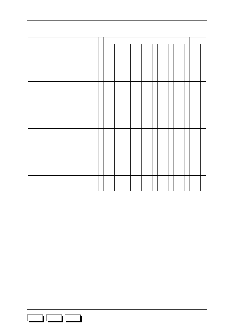
Appendix-48
ML63187/189B/193 User's Manual
Appendix F
M187
M189B
M193
Mask Operation Instructions (continued)
15
INSTRUCTION CODE
FLAG
MNEMONIC
OPERATION
W C
14 13 12 11 10 9 8 7 6 5 4 3 2 1 0 Z C G
0
MSET •cur,#m
Setting of all bits in cur
not masked by #m,
A
®cur
1 1
1 1 0 m
3
m
2
m
1
m
0
r
7
r
6
r
5
r
4
r
3
r
2
r
1
r
0
˜ -- --
0
MSET [HL],#m
Setting of all bits in [HL]
not masked by #m,
A
®[HL]
1 1
0 0 0 0 0
1 0 0 1 1 0 m
3
m
2
m
1
m
0
˜ -- --
0
MSET [XY],#m
Setting of all bits in [XY]
not masked by #m,
A
®[XY]
1 1
0 0 0 0 0
1 0 0 1 1 1 m
3
m
2
m
1
m
0
˜ -- --
0
MSET E:[HL],#m
Setting of all bits in E:
[HL] not masked by #m,
A
®E:[HL]
1 1
0 0 0 0 0
1 0 0 1 0 0 m
3
m
2
m
1
m
0
˜ -- --
0
MSET E:[XY],#m
Setting of all bits in E:
[XY] not masked by #m,
A
®E:[XY]
1 1
0 0 0 0 0
1 0 0 1 0 1 m
3
m
2
m
1
m
0
˜ -- --
0
MSET [HL+],#m
Setting of all bits in [HL]
not masked by #m,
A
®[HL],HL®HL+1
1 1
0 0 0 0 0
1 1 0 1 1 0 m
3
m
2
m
1
m
0
˜ -- ˜
0
MSET [XY+],#m
Setting of all bits in [XY]
not masked by #m,
A
®[XY],XY®XY+1
1 1
0 0 0 0 0
1 1 0 1 1 1 m
3
m
2
m
1
m
0
˜ -- ˜
0
MSET E:[HL+],
#m
Setting of all bits in E:
[HL] not masked by #m,
A
®E:[HL],HL®HL+1
1 1
0 0 0 0 0
1 1 0 1 0 0 m
3
m
2
m
1
m
0
˜ -- ˜
0
MSET E:[XY+],
#m
Setting of all bits in E:
[XY] not masked by #m,
A
®E:[XY],XY®XY+1
1 1
0 0 0 0 0
1 1 0 1 0 1 m
3
m
2
m
1
m
0
˜ -- ˜
Appendix-49
ML63187/189B/193 User's Manual
Appendix F
M187
M189B
M193
Mask Operation Instructions (continued)
15
INSTRUCTION CODE
FLAG
MNEMONIC
OPERATION
W C
14 13 12 11 10 9 8 7 6 5 4 3 2 1 0 Z C G
0
MNOT •cur,#m
Inverting of all bits in
cur not masked by #m,
A
®cur
1 1
1 1 1 m
3
m
2
m
1
m
0
r
7
r
6
r
5
r
4
r
3
r
2
r
1
r
0
˜ -- --
0
MNOT [HL],#m
Inverting of all bits in
[HL] not masked by #m,
A
®[HL]
1 1
0 0 0 0 0
0 0 0 1 1 0 m
3
m
2
m
1
m
0
˜ -- --
0
MNOT [XY],#m
Inverting of all bits in
[XY] not masked by #m,
A
®[XY]
1 1
0 0 0 0 0
0 0 0 1 1 1 m
3
m
2
m
1
m
0
˜ -- --
0
MNOT E:[HL],#m
Inverting of all bits in E:
[HL] not masked by #m,
A
®E:[HL]
1 1
0 0 0 0 0
0 0 0 1 0 0 m
3
m
2
m
1
m
0
˜ -- --
0
MNOT E:[XY],#m
Inverting of all bits in E:
[XY] not masked by #m,
A
®E:[XY]
1 1
0 0 0 0 0
0 0 0 1 0 1 m
3
m
2
m
1
m
0
˜ -- --
0
MNOT [HL+],#m
Inverting of all bits in
[HL] not masked by #m,
A
®[HL],HL®HL+1
1 1
0 0 0 0 0
0 1 0 1 1 0 m
3
m
2
m
1
m
0
˜ -- ˜
0
MNOT [XY+],#m
Inverting of all bits in
[XY] not masked by #m,
A
®[XY],XY®XY+1
1 1
0 0 0 0 0
0 1 0 1 1 1 m
3
m
2
m
1
m
0
˜ -- ˜
0
MNOT E:[HL+],
#m
Inverting of all bits in E:
[HL] not masked by #m,
A
®E:[HL],HL®HL+1
1 1
0 0 0 0 0
0 1 0 1 0 0 m
3
m
2
m
1
m
0
˜ -- ˜
0
MNOT E:[XY+],
#m
Inverting of all bits in E:
[XY] not masked by #m,
A
®E:[XY],XY®XY+1
1 1
0 0 0 0 0
0 1 0 1 0 1 m
3
m
2
m
1
m
0
˜ -- ˜

Appendix-50
ML63187/189B/193 User's Manual
Appendix F
M187
M189B
M193
Bit Operation Instructions
15
INSTRUCTION CODE
FLAG
MNEMONIC
OPERATION
W C
14 13 12 11 10 9 8 7 6 5 4 3 2 1 0 Z C G
1
BTST •cur.n
Bit testing of cur.n
1 1
0 1 1 n
3
n
2
n
1
n
0
r
7
r
6
r
5
r
4
r
3
r
2
r
1
r
0
˜ -- --
0
BTST [HL].n
Bit testing of [HL].n
1 1
0 0 0 0 1
0 0 1 0 1 0 n
3
n
2
n
1
n
0
˜ -- --
0
BTST [XY].n
Bit testing of [XY].n
1 1
0 0 0 0 1
0 0 1 0 1 1 n
3
n
2
n
1
n
0
˜ -- --
0
BTST E:[HL].n
Bit testing of E:[HL].n
1 1
0 0 0 0 1
0 0 1 0 0 0 n
3
n
2
n
1
n
0
˜ -- --
0
BTST E:[XY].n
Bit testing of E:[XY].n
1 1
0 0 0 0 1
0 0 1 0 0 1 n
3
n
2
n
1
n
0
˜ -- --
0
BTST [HL+].n
Bit testing of [HL].n,
HL
®HL+1
1 1
0 0 0 0 1
0 1 1 0 1 0 n
3
n
2
n
1
n
0
˜ -- ˜
0
BTST [XY+].n
Bit testing of [XY].n,
XY
®XY+1
1 1
0 0 0 0 1
0 1 1 0 1 1 n
3
n
2
n
1
n
0
˜ -- ˜
0
BTST E:[HL+].n
Bit testing of E:[HL].n,
HL
®HL+1
1 1
0 0 0 0 1
0 1 1 0 0 0 n
3
n
2
n
1
n
0
˜ -- ˜
0
BTST E:[XY+].n
Bit testing of E:[XY].n,
XY
®XY+1
1 1
0 0 0 0 1
0 1 1 0 0 1 n
3
n
2
n
1
n
0
˜ -- ˜
0
BCLR •cur.n
cur.n
®0,A®cur
1 1
1 0 1 n
3
n
2
n
1
n
0
r
7
r
6
r
5
r
4
r
3
r
2
r
1
r
0
˜ -- --
0
BCLR [HL].n
[HL].n
®0,A®[HL]
1 1
0 0 0 0 1
0 0 0 1 1 0 n
3
n
2
n
1
n
0
˜ -- --
0
BCLR [XY].n
[XY].n
®0,A®[XY]
1 1
0 0 0 0 1
0 0 0 1 1 1 n
3
n
2
n
1
n
0
˜ -- --
0
BCLR E:[HL].n
E:[HL].n
®0,A®E:[HL]
1 1
0 0 0 0 1
0 0 0 1 0 0 n
3
n
2
n
1
n
0
˜ -- --
0
BCLR E:[XY].n
E:[XY].n
®0,A®E:[XY]
1 1
0 0 0 0 1
0 0 0 1 0 1 n
3
n
2
n
1
n
0
˜ -- --
0
BCLR [HL+].n
[HL].n
®0,A®[HL],
HL
®HL+1
1 1
0 0 0 0 1
0 1 0 1 1 0 n
3
n
2
n
1
n
0
˜ -- ˜
0
BCLR [XY+].n
[XY].n
®0,A®[XY],
XY
®XY+1
1 1
0 0 0 0 1
0 1 0 1 1 1 n
3
n
2
n
1
n
0
˜ -- ˜
0
BCLR E:[HL+].n
E:[HL].n
®0,A®E:[HL],
HL
®HL+1
1 1
0 0 0 0 1
0 1 0 1 0 0 n
3
n
2
n
1
n
0
˜ -- ˜
0
BCLR E:[XY+].n
E:[XY].n
®0,A®E:[XY],
XY
®XY+1
1 1
0 0 0 0 1
0 1 0 1 0 1 n
3
n
2
n
1
n
0
˜ -- ˜
0
BSET •cur.n
cur.n
®1,A®cur
1 1
1 1 0 n
3
n
2
n
1
n
0
r
7
r
6
r
5
r
4
r
3
r
2
r
1
r
0
˜ -- --
0
BSET [HL].n
[HL].n
®1,A®[HL]
1 1
0 0 0 0 0
1 0 0 1 1 0 n
3
n
2
n
1
n
0
˜ -- --
0
BSET [XY].n
[XY].n
®1,A®[XY]
1 1
0 0 0 0 0
1 0 0 1 1 1 n
3
n
2
n
1
n
0
˜ -- --
0
BSET E:[HL].n
E:[HL].n
®1,A®E:[HL]
1 1
0 0 0 0 0
1 0 0 1 0 0 n
3
n
2
n
1
n
0
˜ -- --
0
BSET E:[XY].n
E:[XY].n
®1,A®E:[XY]
1 1
0 0 0 0 0
1 0 0 1 0 1 n
3
n
2
n
1
n
0
˜ -- --
0
BSET [HL+].n
[HL].n
®1,A®[HL],
HL
®HL+1
1 1
0 0 0 0 0
1 1 0 1 1 0 n
3
n
2
n
1
n
0
˜ -- ˜
0
BSET [XY+].n
[XY].n
®1,A®[XY],
XY
®XY+1
1 1
0 0 0 0 0
1 1 0 1 1 1 n
3
n
2
n
1
n
0
˜ -- ˜
0
BSET E:[HL+].n
E:[HL].n
®1,A®E:[HL],
HL
®HL+1
1 1
0 0 0 0 0
1 1 0 1 0 0 n
3
n
2
n
1
n
0
˜ -- ˜
0
BSET E:[XY+].n
E:[XY].n
®1,A®E:[XY],
XY
®XY+1
1 1
0 0 0 0 0
1 1 0 1 0 1 n
3
n
2
n
1
n
0
˜ -- ˜

Appendix-51
ML63187/189B/193 User's Manual
Appendix F
M187
M189B
M193
Bit Operation Instructions (continued)
15
INSTRUCTION CODE
FLAG
MNEMONIC
OPERATION
W C
14 13 12 11 10 9 8 7 6 5 4 3 2 1 0 Z C G
0
BNOT •cur.n
cur.n
®cur.n,A®cur
1 1
1 1 1 n
3
n
2
n
1
n
0
r
7
r
6
r
5
r
4
r
3
r
2
r
1
r
0
˜ -- --
0
BNOT [HL].n
[HL].n
®[HL].n,A®[HL] 1 1
0 0 0 0 0
0 0 0 1 1 0 n
3
n
2
n
1
n
0
˜ -- --
0
BNOT [XY].n
[XY].n
®[XY].n,A®[XY] 1 1
0 0 0 0 0
0 0 0 1 1 1 n
3
n
2
n
1
n
0
˜ -- --
0
BNOT E:[HL].n
E:[HL].n
®E:[HL].n,A®
E:[HL]
1 1
0 0 0 0 0
0 0 0 1 0 0 n
3
n
2
n
1
n
0
˜ -- --
0
BNOT E:[XY].n
E:[XY].n
®E:[XY].n,A®
E:[XY]
1 1
0 0 0 0 0
0 0 0 1 0 1 n
3
n
2
n
1
n
0
˜ -- --
0
BNOT [HL+].n
[HL].n
®[HL].n,A®[HL],
HL
®HL+1
1 1
0 0 0 0 0
0 1 0 1 1 0 n
3
n
2
n
1
n
0
˜ -- ˜
0
BNOT [XY+].n
[XY].n
®[XY].n,A®[XY],
XY
®XY+1
1 1
0 0 0 0 0
0 1 0 1 1 1 n
3
n
2
n
1
n
0
˜ -- ˜
0
BNOT E:[HL+].n
E:[HL].n
®E:[HL].n,A®
E:[HL],HL
®HL+1
1 1
0 0 0 0 0
0 1 0 1 0 0 n
3
n
2
n
1
n
0
˜ -- ˜
0
BNOT E:[XY+].n
E:[XY].n
®E:[XY].n,A®
E:[XY],XY
®XY+1
1 1
0 0 0 0 0
0 1 0 1 0 1 n
3
n
2
n
1
n
0
˜ -- ˜
Appendix-52
ML63187/189B/193 User's Manual
Appendix F
M187
M189B
M193
ROM Table Reference Instructions
15
INSTRUCTION CODE
FLAG
MNEMONIC
OPERATION
W C
14 13 12 11 10 9 8 7 6 5 4 3 2 1 0 Z C G
0
MOVHB [HL],
[RA]
[HL],[HL+1]
®(RA)
15-8
1 2
0 0 0 0 0
1 1 0 0 1 0 0 0 1 0 -- -- --
0
MOVHB [XY],
[RA]
[XY],[XY+1]
®(RA)
15-8
1 2
0 0 0 0 0
1 1 0 0 1 1 0 0 1 0 -- -- --
0
MOVHB E:[HL],
[RA]
E:[HL],E:[HL+1]
®
(RA)
15-8
1 2
0 0 0 0 0
1 1 0 0 0 0 0 0 1 0 -- -- --
0
MOVHB E:[XY],
[RA]
E:[XY],E:[XY+1]
®
(RA)
15-8
1 2
0 0 0 0 0
1 1 0 0 0 1 0 0 1 0 -- -- --
0
MOVHB [HL+],
[RA]
[HL],[HL+1]
®(RA)
15-8
,
HL
®HL+2
1 2
0 0 0 0 0
1 1 0 0 1 0 1 0 1 0 -- --
˜
0
MOVHB [XY+],
[RA]
[XY],[XY+1]
®(RA)
15-8
,
XY
®XY+2
1 2
0 0 0 0 0
1 1 0 0 1 1 1 0 1 0 -- --
˜
0
MOVHB E:[HL+],
[RA]
E:[HL],E:[HL+1]
®
(RA)
15-8
,HL
®HL+2
1 2
0 0 0 0 0
1 1 0 0 0 0 1 0 1 0 -- --
˜
0
MOVHB E:[XY+],
[RA]
E:[XY],E:[XY+1]
®
(RA)
15-8
,XY
®XY+2
1 2
0 0 0 0 0
1 1 0 0 0 1 1 0 1 0 -- --
˜
0
MOVHB [HL],
cadr16
[HL],[HL+1]
®
(cadr16)
15-8
2 3
0 0 0 0 0
1 1 0 0 1 0 0 1 0 0
-- -- --
a
15
a
14
a
13
a
12
a
11
a
10
a
9
a
8
a
7
a
6
a
5
a
4
a
3
a
2
a
1
a
0
0
MOVHB [XY],
cadr16
[XY],[XY+1]
®
(cadr16)
15-8
2 3
0 0 0 0 0
1 1 0 0 1 1 0 1 0 0
-- -- --
a
15
a
14
a
13
a
12
a
11
a
10
a
9
a
8
a
7
a
6
a
5
a
4
a
3
a
2
a
1
a
0
0
MOVHB E:[HL],
cadr16
E:[HL],E:[HL+1]
®
(cadr16)
15-8
2 3
0 0 0 0 0
1 1 0 0 0 0 0 1 0 0
-- -- --
a
15
a
14
a
13
a
12
a
11
a
10
a
9
a
8
a
7
a
6
a
5
a
4
a
3
a
2
a
1
a
0
0
MOVHB E:[XY],
cadr16
E:[XY],E:[XY+1]
®
(cadr16)
15-8
2 3
0 0 0 0 0
1 1 0 0 0 1 0 1 0 0
-- -- --
a
15
a
14
a
13
a
12
a
11
a
10
a
9
a
8
a
7
a
6
a
5
a
4
a
3
a
2
a
1
a
0
0
MOVHB [HL+],
cadr16
[HL],[HL+1]
®
(cadr16)
15-8
,HL
®HL+2
2 3
0 0 0 0 0
1 1 0 0 1 0 1 1 0 0
-- --
˜
a
15
a
14
a
13
a
12
a
11
a
10
a
9
a
8
a
7
a
6
a
5
a
4
a
3
a
2
a
1
a
0
0
MOVHB [XY+],
cadr16
[XY],[XY+1]
®
(cadr16)
15-8
,XY
®XY+2
2 3
0 0 0 0 0
1 1 0 0 1 1 1 1 0 0
-- --
˜
a
15
a
14
a
13
a
12
a
11
a
10
a
9
a
8
a
7
a
6
a
5
a
4
a
3
a
2
a
1
a
0
0
MOVHB E:[HL+],
cadr16
E:[HL],E:[HL+1]
®
(cadr16)
15-8
,HL
®HL+2
2 3
0 0 0 0 0
1 1 0 0 0 0 1 1 0 0
-- --
˜
a
15
a
14
a
13
a
12
a
11
a
10
a
9
a
8
a
7
a
6
a
5
a
4
a
3
a
2
a
1
a
0
0
MOVHB E:[XY+],
cadr16
E:[XY],E:[XY+1]
®
(cadr16)
15-8
,XY
®XY+2
2 3
0 0 0 0 0
1 1 0 0 0 1 1 1 0 0
-- --
˜
a
15
a
14
a
13
a
12
a
11
a
10
a
9
a
8
a
7
a
6
a
5
a
4
a
3
a
2
a
1
a
0

Appendix-53
ML63187/189B/193 User's Manual
Appendix F
M187
M189B
M193
ROM Table Reference Instructions (continued)
15
INSTRUCTION CODE
FLAG
MNEMONIC
OPERATION
W C
14 13 12 11 10 9 8 7 6 5 4 3 2 1 0 Z C G
0
MOVLB [HL],
[RA]
[HL],[HL+1]
®(RA)
7-0
1 2
0 0 0 0 0
1 1 0 0 1 0 0 0 1 1 -- -- --
0
MOVLB [XY],
[RA]
[XY],[XY+1]
®(RA)
7-0
1 2
0 0 0 0 0
1 1 0 0 1 1 0 0 1 1 -- -- --
0
MOVLB E:[HL],
[RA]
E:[HL],E:[HL+1]
®
(RA)
7-0
1 2
0 0 0 0 0
1 1 0 0 0 0 0 0 1 1 -- -- --
0
MOVLB E:[XY],
[RA]
E:[XY],E:[XY+1]
®
(RA)
7-0
1 2
0 0 0 0 0
1 1 0 0 0 1 0 0 1 1 -- -- --
0
MOVLB [HL+],
[RA]
[HL],[HL+1]
®(RA)
7-0
,
HL
®HL+2
1 2
0 0 0 0 0
1 1 0 0 1 0 1 0 1 1 -- --
˜
0
MOVLB [XY+],
[RA]
[XY],[XY+1]
®(RA)
7-0
,
XY
®XY+2
1 2
0 0 0 0 0
1 1 0 0 1 1 1 0 1 1 -- --
˜
0
MOVLB E:[HL+],
[RA]
E:[HL],E:[HL+1]
®
(RA)
7-0
,HL
®HL+2
1 2
0 0 0 0 0
1 1 0 0 0 0 1 0 1 1 -- --
˜
0
MOVLB E:[XY+],
[RA]
E:[XY],E:[XY+1]
®
(RA)
7-0
,XY
®XY+2
1 2
0 0 0 0 0
1 1 0 0 0 1 1 0 1 1 -- --
˜
0
MOVLB [HL],
cadr16
[HL],[HL+1]
®
(cadr16)
7-0
2 3
0 0 0 0 0
1 1 0 0 1 0 0 1 0 1
-- -- --
a
15
a
14
a
13
a
12
a
11
a
10
a
9
a
8
a
7
a
6
a
5
a
4
a
3
a
2
a
1
a
0
0
MOVLB [XY],
cadr16
[XY],[XY+1]
®
(cadr16)
7-0
2 3
0 0 0 0 0
1 1 0 0 1 1 0 1 0 1
-- -- --
a
15
a
14
a
13
a
12
a
11
a
10
a
9
a
8
a
7
a
6
a
5
a
4
a
3
a
2
a
1
a
0
0
MOVLB E:[HL],
cadr16
E:[HL],E:[HL+1]
®
(cadr16)
7-0
2 3
0 0 0 0 0
1 1 0 0 0 0 0 1 0 1
-- -- --
a
15
a
14
a
13
a
12
a
11
a
10
a
9
a
8
a
7
a
6
a
5
a
4
a
3
a
2
a
1
a
0
0
MOVLB E:[XY],
cadr16
E:[XY],E:[XY+1]
®
(cadr16)
7-0
2 3
0 0 0 0 0
1 1 0 0 0 1 0 1 0 1
-- -- --
a
15
a
14
a
13
a
12
a
11
a
10
a
9
a
8
a
7
a
6
a
5
a
4
a
3
a
2
a
1
a
0
0
MOVLB [HL+],
cadr16
[HL],[HL+1]
®
(cadr16)
7-0
,HL
®HL+2
2 3
0 0 0 0 0
1 1 0 0 1 0 1 1 0 1
-- --
˜
a
15
a
14
a
13
a
12
a
11
a
10
a
9
a
8
a
7
a
6
a
5
a
4
a
3
a
2
a
1
a
0
0
MOVLB [XY+],
cadr16
[XY],[XY+1]
®
(cadr16)
7-0
,XY
®XY+2
2 3
0 0 0 0 0
1 1 0 0 1 1 1 1 0 1
-- --
˜
a
15
a
14
a
13
a
12
a
11
a
10
a
9
a
8
a
7
a
6
a
5
a
4
a
3
a
2
a
1
a
0
0
MOVLB E:[HL+],
cadr16
E:[HL],E:[HL+1]
®
(cadr16)
7-0
,HL
®HL+2
2 3
0 0 0 0 0
1 1 0 0 0 0 1 1 0 1
-- --
˜
a
15
a
14
a
13
a
12
a
11
a
10
a
9
a
8
a
7
a
6
a
5
a
4
a
3
a
2
a
1
a
0
0
MOVLB E:[XY+],
cadr16
E:[XY],E:[XY+1]
®
(cadr16)
7-0
,XY
®XY+2
2 3
0 0 0 0 0
1 1 0 0 0 1 1 1 0 1
-- --
˜
a
15
a
14
a
13
a
12
a
11
a
10
a
9
a
8
a
7
a
6
a
5
a
4
a
3
a
2
a
1
a
0

Appendix-54
ML63187/189B/193 User's Manual
Appendix F
M187
M189B
M193
Stack Operation Instructions
15
INSTRUCTION CODE
FLAG
MNEMONIC
OPERATION
W C
14 13 12 11 10 9 8 7 6 5 4 3 2 1 0 Z C G
0
PUSH HL
(RSP)
®{FLAG,A,HL},
RSP
®RSP+1
1 2
0 0 0 0 0
0 0 0 0 0 1 0 0 0 0 -- -- --
0
PUSH XY
(RSP)
®{CBR,EBR,XY},
RSP
®RSP+1
1 2
0 0 0 0 0
0 0 0 0 0 1 0 0 0 1 -- -- --
0
POP HL
RSP
®RSP≠1,
{FLAG,A,HL}
®(RSP)
1 2
0 0 0 0 0
0 0 0 0 0 1 0 0 1 0
˜ ˜ ˜
0
POP XY
RSP
®RSP≠1,
{CBR,EBR,XY}
®(RSP)
1 2
0 0 0 0 0
0 0 0 0 0 1 0 0 1 1 -- -- --
Flag Operation Instructions
15
INSTRUCTION CODE
FLAG
MNEMONIC
OPERATION
W C
14 13 12 11 10 9 8 7 6 5 4 3 2 1 0 Z C G
0
FCLR G
G
®0
1 1
0 0 0 0 0
0 0 0 0 0 0 0 0 1 0 -- --
˜
0
FCLR C
C
®0
1 1
0 0 0 0 0
0 0 0 0 0 0 0 0 1 1 --
˜ --
0
FCLR Z
Z
®0
1 1
0 0 0 0 0
0 0 0 0 0 0 0 1 0 0
˜ -- --
0
FSET G
G
®1
1 1
0 0 0 0 0
0 0 0 0 0 0 0 1 1 0 -- --
˜
0
FSET C
C
®1
1 1
0 0 0 0 0
0 0 0 0 0 0 0 1 1 1 --
˜ --
0
FSET Z
Z
®1
1 1
0 0 0 0 0
0 0 0 0 0 0 1 0 0 0
˜ -- --
Jump Instructions
15
INSTRUCTION CODE
FLAG
MNEMONIC
OPERATION
W C
14 13 12 11 10 9 8 7 6 5 4 3 2 1 0 Z C G
0
LJMP cadr15
PC
®cadr15
2 2
0 0 0 0 0
0 0 0 0 0 1 0 1 0 0
-- -- --
0 a
14
a
13
a
12
a
11
a
10
a
9
a
8
a
7
a
6
a
5
a
4
a
3
a
2
a
1
a
0
1
JMP cadr12
PC
11~0
®cadr12
1 1
1 1 0 a
11
a
10
a
9
a
8
a
7
a
6
a
5
a
4
a
3
a
2
a
1
a
0
-- -- --
0
SJMP radr8
PC
®Next PC+radr8
1 1
0 0 0 1 0
0 a
7
1 a
6
a
5
a
4
a
3
a
2
a
1
a
0
-- -- --
0
JMP PC+A
PC
®PC+A+1
1 1
0 0 0 0 0
0 0 0 0 0 1 0 1 1 1 -- -- --

Appendix-55
ML63187/189B/193 User's Manual
Appendix F
M187
M189B
M193
Conditional Branch Instructions
Call/Return Instructions
15
INSTRUCTION CODE
FLAG
MNEMONIC
OPERATION
W C
14 13 12 11 10 9 8 7 6 5 4 3 2 1 0 Z C G
BC radr8
if C=1 then
PC
®Next PC+radr8(<)
1 1
-- -- --
0 0 0 0 1 0
1 a
7
0 a
6
a
5
a
4
a
3
a
2
a
1
a
0
BLT radr8
BNC radr8
if C=0 then
PC
®Next PC+radr8( )
1 1
-- -- --
0 0 0 0 1 0
1 a
7
1 a
6
a
5
a
4
a
3
a
2
a
1
a
0
BGE radr8
=
>
BZ radr8
if Z=1 then
PC
®Next PC+radr8(=)
1 1
-- -- --
0 0 0 0 1 1
0 a
7
0 a
6
a
5
a
4
a
3
a
2
a
1
a
0
BEQ radr8
BNZ radr8
if Z=0 then
PC
®Next PC+radr8()
1 1
-- -- --
0 0 0 0 1 1
0 a
7
1 a
6
a
5
a
4
a
3
a
2
a
1
a
0
BNE radr8
if (C=1) (Z=1) then
PC
®Next PC+radr8( )=>
BLE radr8
1 1
-- -- --
0 0 0 0 1 1
1 a
7
0 a
6
a
5
a
4
a
3
a
2
a
1
a
0
if (C=0) (Z=0) then
PC
®Next PC+radr8(>)
BGT radr8
1 1
-- -- --
0 0 0 0 1 1
1 a
7
1 a
6
a
5
a
4
a
3
a
2
a
1
a
0
if G=0 then
PC
®Next PC+radr8
BNG radr8
1 1
-- -- --
0 0 0 0 1 0
0 a
7
0 a
6
a
5
a
4
a
3
a
2
a
1
a
0
15
INSTRUCTION CODE
FLAG
MNEMONIC
OPERATION
W C
14 13 12 11 10 9 8 7 6 5 4 3 2 1 0 Z C G
LCAL cadr15
2 2
-- -- --
0 a
14
a
13
a
12
a
11
a
10
a
9
a
8
a
7
a
6
a
5
a
4
a
3
a
2
a
1
a
0
0 0 0 0 0 0
0 0 0 0 0 1 0 1 0 1
(SP)
®PC,PC®cadr15,
SP
®SP+1
(SP)
®PC,PC
11-0
®
cadr12,SP
®SP+1
CAL cadr12
1 1 1 1 1 1 a
11
a
10
a
9
a
8
a
7
a
6
a
5
a
4
a
3
a
2
a
1
a
0
-- -- --
PC
®(SP)+1,SP®SP≠1
RT
1 1 0 0 0 0 0 0
0 0 0 0 0 0 1 0 1 1 -- -- --
PC
®(SP)+1,SP®SP≠1,
MIE
®1
RTI
1 1 0 0 0 0 0 0
0 0 0 0 0 0 1 1 0 0 -- -- --
PC
®(SP)+1,SP®SP≠1
MIE
®status of MIE
before an interrupt
occurs
RTNMI
1 1 0 0 0 0 0 0
0 0 0 0 0 0 1 1 0 1 -- -- --

Appendix-56
ML63187/189B/193 User's Manual
Appendix F
M187
M189B
M193
Control Instructions
15
INSTRUCTION CODE
FLAG
MNEMONIC
OPERATION
W C
14 13 12 11 10 9 8 7 6 5 4 3 2 1 0 Z C G
NOP
1 1
-- -- --
0 0 0 0 0 0
0 0 0 0 0 0 0 0 0 0
NO OPERATION
HALT
1 1
-- -- --
0 0 0 0 0 0
0 0 0 0 0 0 0 0 0 1
HALT CPU
EI
1 1
-- -- --
0 0 0 0 0 0
0 0 0 0 0 0 1 1 1 0
MIE
®1
DI
1 1
-- -- --
0 0 0 0 0 0
0 0 0 0 0 0 1 1 1 1
MIE
®0
INCB HL
1 1
-- --
˜
0 0 0 0 0 0
0 0 0 0 0 1 1 0 0 0
HL
®HL+1
INCB XY
1 1
-- --
˜
0 0 0 0 0 0
0 0 0 0 0 1 1 0 0 1
XY
®XY+1
INCW RA
1 1
-- --
˜
0 0 0 0 0 0
0 0 0 0 0 1 1 0 1 0
RA
®RA+1
MOV CBR,#i4
1 1
-- -- --
0 0 0 0 0 0
0 0 0 0 1 1 i
3
i
2
i
1
i
0
CBR
®i4
MOV EBR,#i4
1 1
-- -- --
0 0 0 0 0 0
0 0 0 0 1 0 i
3
i
2
i
1
i
0
EBR
®i4
MOV RA0,#i4
1 1
-- -- --
0 0 0 0 0 0
1 0 0 0 0 0 i
3
i
2
i
1
i
0
RA0
®i4
MOV RA1,#i4
1 1
-- -- --
0 0 0 0 0 0
1 0 0 0 0 1 i
3
i
2
i
1
i
0
RA1
®i4
MOV RA2,#i4
1 1
-- -- --
0 0 0 0 0 0
1 0 0 0 1 0 i
3
i
2
i
1
i
0
RA2
®i4
MOV RA3,#i4
1 1
-- -- --
0 0 0 0 0 0
1 0 0 0 1 1 i
3
i
2
i
1
i
0
RA3
®i4
MOV H,#i4
1 1
-- -- --
0 0 0 0 0 0
0 1 0 0 1 1 i
3
i
2
i
1
i
0
H
®i4
MOV L,#i4
1 1
-- -- --
0 0 0 0 0 0
0 1 0 0 1 0 i
3
i
2
i
1
i
0
L
®i4
MOV X,#i4
1 1
-- -- --
0 0 0 0 0 0
0 1 0 0 0 1 i
3
i
2
i
1
i
0
X
®i4
MOV Y,#i4
1 1
-- -- --
0 0 0 0 0 0
0 1 0 0 0 0 i
3
i
2
i
1
i
0
Y
®i4
MSA cadr15
2 3
-- -- --
0 0 0 0 0 0
0 0 0 0 0 1 0 1 1 0
Melody output starts
0 a
14
a
13
a
12
a
11
a
10
a
9
a
8
a
7
a
6
a
5
a
4
a
3
a
2
a
1
a
0

Appendix-57
ML63187/189B/193 User's Manual
Appendix G
M187
M189B
M193
Appendix G Mask Option
In the ML63187, ML63189B, and ML63193, use the mask option to specify the following
functions:
∑ Low-speed clock oscillation circuit
Specify the crystal oscillation circuit or the RC oscillation circuit for the low-speed clock
oscillation circuit.
∑ Reset signal sampling
Specify whether or not the reset signal will be sampled at 2 kHz.
When specifying "will carry out 2 kHz sampling," hold the RESET pin at a "H" level for
1 ms or more.
To use the mask option, assign mask option data in the application program in accordance
with the formats below. The mask option area for each device is an application program
execution disabled area.
∑ Mask option area for ML63187:
3FE0H
∑ Mask option area for ML63189B: 7FE0H
∑ Mask option area for ML63193:
0FFE0H
Mask option data assignment format
The mask option is set with the two bits (bits 0 and 1) addressed in the mask option area that
is assigned to each model.
Table G-1 shows the mask option data assignment format.
Table G-1 Mask Option Data Assignment Format
Example of mask option data generation
∑ When the crystal oscillation circuit is specified for the low-speed clock oscillation circuit and
not carrying out reset signal sampling is specified in the ML63187
ORG
3FE0H
®
Use an assembler pseudo-instruction to set the address of option data
to 3FE0H.
DW
0002H
:
Crystal oscillation circuit, 2 kHz sampling will not be carried out
∑ When the RC oscillation circuit is specified for the low-speed clock oscillation circuit and
carrying out reset signal sampling is specified in the ML63189B
ORG
7FE0H
®
Use an assembler pseudo-instruction to set the address of option data
to 7FE0H.
DW
0001H
:
RC oscillation circuit, 2 kHz sampling will be carried out
Function
Low-speed clock oscillation circuit
(crystal oscillation circuit/RC oscillation circuit)
data
Crystal oscillation circuit
Mask option area
ML63187: 3FE0H
ML63189B: 7FE0H
ML63193: 0FFE0H
0
Will carry out 2 kHz sampling
0
RC oscillation circuit
1
Will not carry out 2 kHz sampling
1
Option to be selected
bit
bit 0
bit 1
Reset signal sampling
(will/will not carry out 2 kHz sampling)

Appendix-58
ML63187/189B/193 User's Manual
Appendix G
M187
M189B
M193
∑ When the crystal oscillation circuit is specified for the low-speed clock oscillation circuit and
carrying out reset signal sampling is specified in the ML63193
ORG
0FFE0H
®
Use an assembler pseudo-instruction to set the address of option data
to 0FFE0H.
DW
0000H
:
Crystal oscillation circuit, 2 kHz sampling will be carried out
[Additional note: Handling of mask option area when the Development Support System
(EASE63180) is used]
The Development Support System (EASE63180) allows the user to execute application
programs in the mask option area as well as reading and writing data there. What this means
is that there is no equivalent to the test data N area break for detecting when execution strays
into this area. The developer must, therefore, define breakpoints for the mask option area
when using the EASE63180. These breakpoints then prevent program execution in this area
in a manner similar to the test data N area break.

ML63187/189B/193
User's Manual
First Edition:
March 2000
©
©
©
©
© 2000 Oki Electric Industry Co., Ltd.
FEUL63193-01


