 | –≠–ª–µ–∫—Ç—Ä–æ–Ω–Ω—ã–π –∫–æ–º–ø–æ–Ω–µ–Ω—Ç: ML63295A | –°–∫–∞—á–∞—Ç—å:  PDF PDF  ZIP ZIP |

FEDL63295A-02
1Semiconductor
This version: Jul. 2001
Previous version: Nov. 2000
ML63295A
4-Bit Microcontroller with Built-in 3072-Dot Matrix LCD Driver and Melody Circuit
1/38
GENERAL DESCRIPTION
The ML63295A is a CMOS 4-bit microcontroller that employs Oki's original CPU core nX-4/250.
The ML63295A operates on a power supply voltage of 6 V.
With built-in 3072-dot matrix LCD drivers (96 SEG.
◊
32 COM.), the ML63295A is suited for applications such as
electronic dictionaries with an LCD.
FEATURES
∑ Extensive instruction set
439 instructions:
Transfer, rotate, increment/decrement, arithmetic operations, compare, logic operations, mask operations,
bit operations, ROM table reference, external memory transfer, stack operations, flag operations, jump,
conditional branch, call/return, control
∑ Wide variety of addressing modes
Indirect addressing mode for 4 types of data memory with current bank register, extra bank register,
HL register and XY register
Data memory bank internal direct addressing mode
∑ Processing speed
2 clocks per machine cycle, with most instructions executed in 1 machine cycle
Minimum instruction execution time : 61
µ
s (@ 32.768 kHz system clock)
: 1
µ
s (@ 2 MHz system clock)
∑ Clock generation circuit
Low-speed clock : Crystal oscillation or RC oscillation selected with mask option
(30 kHz to 80 kHz)
High-speed clock: Ceramic oscillation or RC oscillation selected with software
(2 MHz max)
∑ Program memory space
32 K words
Basic instruction length is 16 bits/1word.
∑ Data memory space
2048 nibbles
∑ External data memory space
64 Kbytes (expandable furthermore by using the I/O ports)
∑ Stack level
Call stack level
: 16 levels
Register stack level
: 16 levels

FEDL63295A-02
1Semiconductor
ML63295A
2/38
∑ Ports
Input ports:
Selectable as input pull-up resistor/input pull-down resistor/high impedance input.
Output ports:
Selectable as P-channel open drain output/N-channel open drain output/high-impedance output/CMOS
output.
I/O ports:
Selectable as input pull-up resistor/input pull-down resistor/high impedance input.
Selectable as P-channel open drain output/N-channel open drain output/high-impedance output/
CMOS output.
Can be interfaced with external peripherals that use a different power supply than this device uses.
Number of ports:
Input port
: 2 ports ◊ 4 bits
Output port
: 6 ports ◊ 4 bits
Input-output port
: 6 ports ◊ 4 bits
∑ Melody output
Melody frequency
: 529 Hz to 2979 Hz
Tone length
: 63 varieties
Tempo
: 15 varieties
Melody data
: Stored in program memory
Buzzer driver signal output
: 4 kHz
∑ LCD driver
Number of segments
: 3072 Max. (96 SEG. ◊ 32 COM.)
Duty
: Selectable as 1/2, 1/4, 1/6, 1/8, 1/10, 1/12, 1/14, 1/16, 1/18, 1/20,
1/22, 1/24, 1/26, 1/28, 1/30, or 1/32 duty
Bias
: Selectable as 1/5 or 1/6 bias (regulator built-in)
Frame frequency
: ex. 64 Hz (at 1/32 duty), 128 Hz (at 1/16 duty), 256 Hz (at 1/8
duty), 512 Hz (at 1/4 duty), 1024 Hz (at 1/2 duty)
Contrast
: 16 levels adjustable
Display
modes
: Selectable as all-ON mode/all-OFF mode/power down
mode/normal display mode
∑ Multiplier/divider circuit
Multiplier
: (8 bits)
◊
(8 bits)
Product (16 bits)
Divider
: (16 bits)
/
(8 bits)
Quotient (16 bits), Remainder (8 bits)
∑ System reset function
System reset through RESET pin
System reset by power-on detection
System reset by low-speed oscillation halt
∑ Battery check
Low-voltage supply check
The value of the judgment voltage is selected by the software (by setting the LD1 and LD0 bits of
BLDCON).
LD1
LD0
Judgment voltage (V)
Remarks
1
0
4.5
±
0.1
Ta = 25
∞
C
1
1
5.1
±
0.1
Ta = 25
∞
C

FEDL63295A-02
1Semiconductor
ML63295A
3/38
∑ Timers and Counter
8-bit timer
: 2
Selectable as auto-reload mode/clock frequency measurement
mode
Watchdog timer
: 1
100 Hz timer
: 1
Measurable in steps of 1/100 sec.
15-bit time-base counter
: 1
1, 2, 4, 8, 16, 32, 64, and 128 Hz signals can be read
∑ Serial port
Mode
: Selectable as UART mode, synchronous mode
UART communication speed
: 1200 bps, 2400 bps, 4800 bps, 9600 bps
Clock frequency in synchronous mode : Internal clock mode (32.768 kHz), External clock frequency
Data length
: 5 to 8 bits
∑ Shift register
Shift clock
: 1
◊
or 1/2
◊
system clock, external clock
Data length
: 8 bits
∑ Interrupt factors
External interrupt
: 5
Internal interrupt
: 12
∑ Operating temperature
: ≠20 to +70
∞
C
∑ Power supply voltage
: 3.5 to 7.2 V
∑ Package:
Chip (212 pads)
: (Product name: ML63295A-xxxWA)
240-pin plastic QFP (QFP240-P-3232-0.50-BK4) : (Product name: ML63295A-xxxGA)
....under consideration
xxx indicates a code number.
FEDL63295A-02
1Semiconductor
ML63295A
4/38
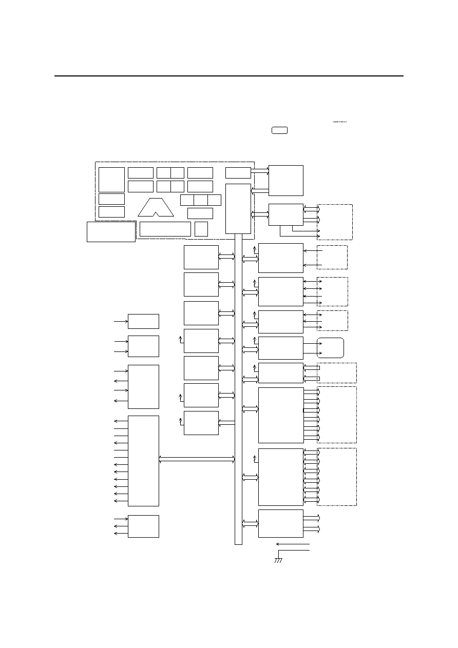
BLOCK DIAGRAM
Asterisks (*) indicate the port secondary functions. Signal names enclosed by chain lines ( ) indicate interface
signals of the V
DDI
power supply system. Signal names enclosed by indicates signals of the V
DDE
power
supply system.
nX-4/250
TIMING
CONT.
CBR
EBR
H
L
X
Y
RA
MIE
A
INSTRUCTION
DECODER
IR
BUS
CONT.
ROM
32 KW
SP
RSP
C
G
Z
STACK
CAL.S:16-level
REG.S:16-level
PC
ALU
TBC
RST
TST
XT0
XT1
OSC0
OSC1
OSC
RESET
MELODY
I/O
PORT
OUTPUT
INT
4
INT
4
TST2
DA
TA
B
U
S
BLD
W DT
INT
1
TST1
100HzTC
INT
1
V
DDX1
BIAS
EXTMEM
64 KB
D0-7*
A0-15*
R D *
W R *
MD
MDB
P8.0-P8.3
P9.0-P9.3
PA.0-PA.3
P2.0-P2.3
P3.0-P3.3
P4.0-P4.3
P5.0-P5.3
LCD
&
DSPR
COM1-COM32
SEG0-SEG95
V
DDI
V
SS
PB.0-PB.3
PC.0-PC.3
TIMER
8 bit (2ch)
INT
2
T2CK*
T3CK*
SIO
RXC*
TXC*
INT
2
RXD*
TXD*
PE.0-PE.3
P6.0-P6.3
P7.0-P7.3
MULDIV
SFT
SCLK*
SOUT*
SIN*
INPUT
PORT
INT
1
P0.0-P0.3
P1.0-P1.3
INT
1
INT
1
RAM
2048N
INT
VR
V
DDL
V
DD
V
DDX2
V
DDX3
V
DDX4
C1
C2
V
DD1
V
DD2
V
DD3
V
DD4
V
DD5
V
DD6
V
DDE
CPU core

FEDL63295A-02
1Semiconductor
ML63295A
5/38
PIN CONFIGURATION (TOP VIEW)
1 2 3 4 5 6 7 8 9 10 11 12 13 14 15 16 17 18 19 20 21 22 23 24 25 26
P9.1
27 28 29
P9.0
P8.3
P8.2
30
P8.0
31
P7.3
32
P7.2
33 34 35
P7.1
P7.0
P6.3
36 37 38
P6.2
P6.1
(NC)
COM32
V
SS
V
DD1
V
DD2
COM27
COM28
COM29
COM31
COM23
COM24
COM25
COM26
170 169 168
147
173 172 171
240
239
238
237
236
235
234
233
232
231
230
229
228
227
226
225
224
223
222
221
220
219
218
217
216
215
61
62
63
64
65
66
67
68
69
70
71
72
73
74
75
76
77
78
79
80
81
82
83
84
85
86
39 40 41 42 43 44
PA.3
PA.2
87
88
89
90
91
92
93
94
95
96
97
98
99
100
101
102
103
104
156 155 154 153 152 151 150 149 148
167 166 165 164 163 162 161 160 159 158 157
178 177 176
179
175 174
214
213
212
211
210
209
208
206
205
204
203
202
201
200
199
198
197
196
SEG70
SEG71
SEG65
SEG66
SEG67
SEG60
SEG61
SEG62
SEG63
SEG45
SEG46
SEG47
(NC)
SEG64
SEG68
SEG69
COM18
SEG43
SEG42
SEG40
SEG39
SEG38
SEG37
SEG36
(NC)
(NC)
SEG41
V
DD5
V
DD6
V
DDX1
V
DDX2
V
DDX3
V
DDX4
C1
C2
V
DD
V
DDL
V
DD
V
DDE
OSC1
OSC0
P6.0
P5.3
P5.2
P5.1
P5.0
P4.3
P4.2
P4.1
P4.0
P3.3
P3.2
P3.1
P3.0
P2.3
SEG58
SEG59
SEG53
SEG54
SEG55
SEG48
SEG49
SEG51
SEG44
SEG52
SEG56
SEG57
SEG50
TST1
TST2
V
DD3
XT1
XT0
RESET
MD
MDB
V
DDI
P2.0
P1.3
P1.2
P1.1
P1.0
P0.3
(NC)
(NC)
P2.1
P2.2
COM19
COM20
COM21
COM22
PA.1
PA.0
P9.3
P9.2
V
DD4
45 46 47 48 49 50 51 52 53 54 55 56 57 58 59 60
COM1 COM2 COM3 COM4 COM5 COM6 COM7
COM9 COM10 COM11 COM12 COM13 COM14
COM8
SEG14 SEG15 SEG16 SEG17
SEG19 SEG20
SEG22 SEG23
SEG18
COM15 COM16
SEG0 SEG1 SEG2 SEG3 SEG4 SEG5 SEG6 SEG7 SEG8 SEG9 SEG10 SEG11 SEG12 SEG13
P0.2 P0.1 P0.0 V
SS
SEG21
SEG24 SEG25 SEG26 SEG27 SEG28 SEG29 SEG30 SEG31 SEG32
(NC) (NC)
(NC) (NC)
105
106
107
108
109
110
111
112
113
114
115
116
117
118
119
120
(NC)
(NC)
SEG81
SEG82
SEG83
SEG76
SEG77
SEG78
SEG79
SEG80
SEG84
SEG85
SEG74
SEG75
SEG72
SEG73
(NC)
SEG93
SEG94
SEG95
COM17
SEG90
SEG91
SEG92
134
135
(NC)
127 126 125 124 123 122 121
133 132 131 130 129 128
142 141 140 139 138 137 136
146 145 144 143
1
8
0
(NC)
PB.3
PB.2
PB.1
PB.0
PE.1
PE.0
194
193
192
191
190
189
188
187
186
PC.3
PC.2
PC.1
PC.0
195
185
184
183
182
181
(NC)
(NC)
(NC)
PE.3
PE.2
207
P8.1
COM30
(NC)
(NC)
(NC)
(NC)
(NC)
(NC) (NC) (NC) (NC)
(NC)
SEG33 SEG34 SEG35
SEG86
SEG87
SEG88
SEG89
240-Pin Plastic QFP
(GA:QFP240-P-3232-0.50-BK4)
Note: Pins marked as (NC) are no-connection pins which are left open.