OKI Semiconductor
FEDL675001-01
Issue Date: Dec. 15, 2003
ML675001/Q5002/Q5003
32-bit ARM-Based General-Purpose Microcontroller
ARM, ARM7TDMI, Multi-ICE and AMBA are registered trademarks of ARM Ltd., UK.
µPLAT is Oki's trademark.
The contents of this data sheet are subject to change for modification without notice.
1/24
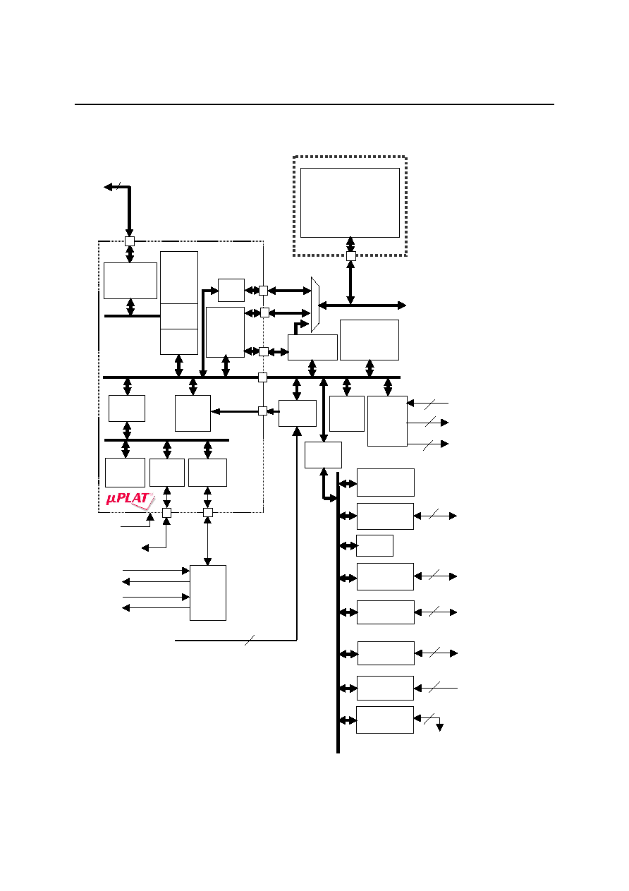
GENERAL DESCRIPTION
The ML675001, ML67Q5002, and ML67Q5003 microcontrollers (MCUs) are the members of an extensive and
growing family of 32-bit ARM
Æ
-based standard products for general-purpose applications that require 32-bit
CPU performance and low cost afforded by MCU integrated features.
ML675001/67Q5002/67Q5003 provide 8KB unified cache memory, built-in 32Kbyte SRAM, built-in 4Kbyte
boot ROM, and a host of other useful peripherals such as auto-reload timers, watchdog timer (WDT),
pulse-width modulators (PWM), A-to-D converter, expanded UARTs, synchronous serial port, I2C serial
interface, GPIOs, DMA controller, external memory controller, and boundary scan capability. In addition, the
ML67Q5002 and ML67Q5003 offer 256 Kbytes and 512 Kbytes of built-in Flash memory respectively. The
ML675001, ML67Q5002 and ML67Q5003 are pin-to-pin compatible with each other, and are pin-to-pin
compatible with ML674001 Series for easy performance updates.
Oki's ML675K Family MCUs are capable of executing both the 32-bit ARM instruction set for
high-performance applications as well as the 16-bit Thumb
Æ
instruction set for high code-density,
power-efficient applications. With an ARM7TDMI
Æ
core operating at 60 MHz maximum frequency, ARM
ThumbTM capabilities, and robust feature sets, the ML675001 Series MCUs are suitable for an array of
applications including high performance industrial controllers and instrumentation, telecom, PC peripherals,
security/surveillance, test equipment, and a variety of consumer electronics devices.
The ARM7TDMI
Æ
Advantage
Oki's ML675K Family of low-cost ARM-based MCUs offers system designers a bridge from 8- and 16-bit
proprietary MCU architectures to ARM's higher-performance, affordable, widely-accepted industry standard
architecture and its industry-wide support infrastructure. The ARM industry infrastructure offers the system
developers many advantages including software compatibility, many ready-to-use software applications, large
choices among hardware and software development tools. These ARM-based advantages allow Oki's
customers to better leverage engineering resources, lower development costs, minimize project risks, and reduce
their product time to market. In addition, migration of a design with an Oki standard MCU to an Oki custom
solution is easily facilitated with its award-winning uPLATTM product development architecture.
FEATURES
∑ CPU
32-bit RISC CPU (ARM7TDMI)
32-bit instructions (ARM Instructions) and 16-bit instructions (Thumb Instructions) mixed
General purpose registers : 31 x 32 bits
Built-in Barrel shifter and multiplier (32 bit x 8 bit, Modified Booth's Algorithm)
Little endian
Built-in debug function
Cache
memory
8KB
unified
memory
4
way
set-associative
∑ Internal memory
RAM
32KB (32-bit access)
FLASH
(16-bit
access)
ML675001 :
ROM-less
version
ML67Q5002
:
256Kbytes
ML67Q5003
:
512Kbytes

FEDL675001-01
OKI Semiconductor
ML675001/67Q5002/67Q5003
2/24
∑ External memory controller
ROM (FLASH): 16 Mbytes
SRAM: 16 Mbytes
DRAM: 64 Mbytes (SDRAM and EDO-DRAM support)
External IO devices: 16 Mbytes x 2 banks, 4 Chip select pins
Wait control input signal for each bank
Independent programmable wait settings for each bank
∑ Interrupt controller
28 sources: 23 internals and 5 externals (IRQ: 4, FIQ: 1)
∑ DMA controller
2 channels: Dual address mode, cycle steal and burst tranfer mode
∑ Timer
1 channel: 16-bit auto reload for operating system
6 channels: 16-bit auto reload for application
1 channel: 16 bit watchdog timer
∑ Serial interface
1 channel: UART
1 channel: UART with 16-byte FIFO
1 channel: synchronous
1 channel: I2C (single master)
∑ Parallel I/O Port
4 ports x 8 bits (bitwise input/output settings)
1 port x 10 bit (bitwise input/output settings)
∑ PWM
2 channels x 16 bits
∑ Analog-to-Digital Converter
4 channels x 10 bits
∑ Power down mechanism
Standby (all clock stop) and Halt (clock stop by each function block)
Clock gear (selectable 1/1, 1/2, 1/4, 1/8, 1/16, 1/32 base clock frequency)
∑ JTAG interface
Connectable to JTAG ICE
∑ Power supply voltage
Core section: 2.25 V to 2.75 V
IO section: 3.0 V to 3.6 V
PLL section: 2.25 V to 2.75 V
Analog section: 3.0 V to 3.6 V
∑ Operating frequency
1-60
MHz
∑ Operating temperature (ambient temperature)
≠40
∞C to +85∞C
∑ Package
144-pin plastic LQFP (LQFP144-P-2020-0.50)
144-pin plastic LFBGA (P-LFBGA144-1111-0.80)

FEDL675001-01
OKI Semiconductor
ML675001/67Q5002/67Q5003
5/24
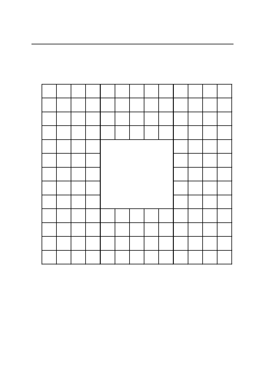
144-Pin Plastic LQFP
(Secondary fun(Primary function)
99
98
97
96
95
94
93
92
91
90
89
88
87
86
85
84
83
82
81
80
79
78
77
76
75
74
73
(Primary functi (Secondary f
PLLVDD
72
XIOCS_N[3]
PLLGND
71
XIOCS_N[2]
CKO
70
XIOCS_N[1]
JSEL
69
GND
TMS
68
XIOCS_N[0]
TCK
67
XRAMCS_N
DRAME_N
66
XROMCS_N
CKOE_N
65
XBWE_N[1]
GND
64
XBWE_N[0]
OSC0
63
XWE_N
OSC1_N
62
VDD_IO
VDD_IO
61
XOE_N
TEST
60
PIOC[7]
XWR
SIN
PIOA[0]
59
PIOC[6]
XA[23]
SOUT
PIOA[1]
58
VDD_CORE
AVDD
57
PIOC[5]
XA[22]
VREFP
56
PIOC[4]
XA[21]
AIN[0]
55
PIOC[3]
XA[20]
AIN[1]
54
VDD_IO
AIN[2]
53
PIOC[2]
XA[19]
AIN[3]
52
XA[18]
VREFN
51
GND
AGND
50
XA[17]
GND
49
XA[16]
CTS
PIOA[2]
48
XA[15]
VDD_IO
47
GND
DSR
PIOA[3]
46
XA[14]
DCD
PIOA[4]
45
XA[13]
VDD_CORE
44
XA[12]
DTR
PIOA[5]
43
XA[11]
RTS
PIOA[6]
42
XA[10]
RI
PIOA[7]
41
VDD_IO
GND
40
XA[9]
SDA
PIOE[3]
39
XA[8]
SCL
PIOE[4]
38
XA[7]
STXD
PIOB[6]
37
XA[6]
1 2 3 4 5 6 7 8 9 10 11 12 13 14 15 16 17 18 19 20 21 22 23 24 25 26 27 28 29 30 31 32 33 34 35 36
XDQM[0]/XCAS_N[0]
XDQM[1]/XCAS_N[1]
DREQ[0]
DREQCLR[0]
DREQCLR[1] DREQ[1]
TDO
nTRST
TCOUT[1]
PWMOUT[0]
PWMOUT[1]
XBS
_
N[0]
XBS
_
N[1]
PIOE[0]
BSEL[0]
BSEL[1]
PIOE[5]
PIOE[1]
PIOE[6]
PIOE[7]
PIOE[8]
PIOE[9]
GND
VDD
_
IO
PIOD[2]
PIOD[5]
PIOB[5]
PIOC[0]
PIOD[0]
PIOD[1]
(
Pri
m
ar
y
f
(
Second
a
PIOB[0] PIOD[7]
TCOUT[0]
XWAIT
PIOC[1]
GND
PIOB[3]
PIOB[4]
PIOD[6]
PIOB[1]
VDD
_
IO
PIOB[2]
XA[5]
VDD
_
IO
SRXD
XCAS
_
N
XRAS
_
N
XSDCLK
XSDCS
_
N
XSDCKE
EXINT[0]
XA[2] XA[3] GND XA[4]
XD[14] XD[15] XA[0] XA[1]
XD[11] XD[12] VDD
_
IO
XD[13]
XD[9] XD[10]
NC
VDD
_
CORE
XD[7] CLKMD1
XD[8]
EXINT[1]
CLKMD0 XD[5] XD[6] GND
PIOD[3]
PIOD[4]
XD[2] XD[3] XD[4] GND
VDD
_
IO
XD[0] XD[1]
EXINT[2]
EXINT[3]
EFIQ
_
N
SCLK
SDI
102
101
TEST1 PIOB[7] FWR RESET
_
N
SDO
100
108
107
106
105
104
103
PIOE[2]
TDI
109
110
111
112
113
114
115
116
117
118
119
120
121
122
123
124
125
126
127
128
129
130
131
132
140
133
134
135
136
(Secondary
function
)
(Primary
function
)
VDD
_
CORE
141
142
143
144
137
138
139
144pin LQFP
(TOP VIEW)
Notes: NC pins are electrically unconnected in the package.
NC pins can be connected to Vdd or GND.