
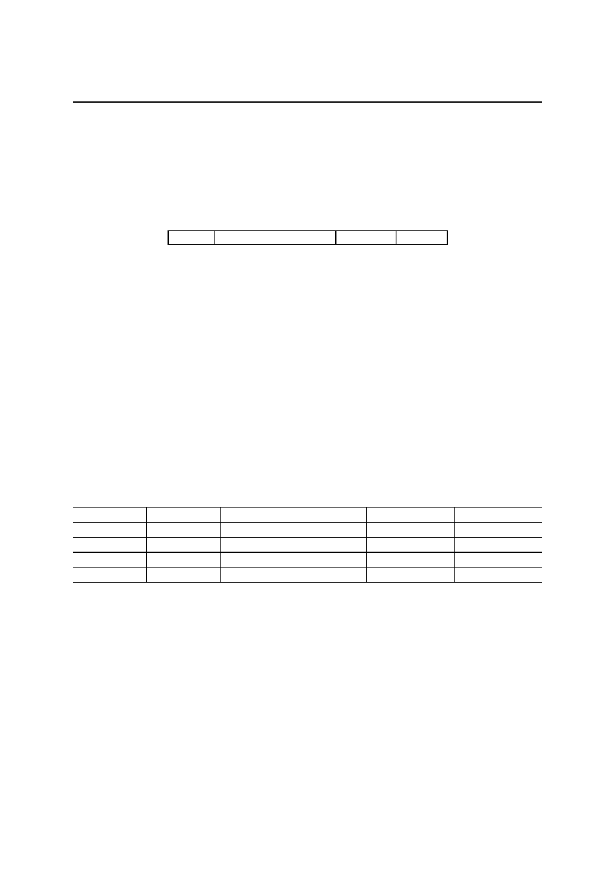
FEDL7012-04-01
1Semiconductor
This version: Sep. 2000
ML7012-04
2400 bps Single Chip Full Duplex Data Modem with Protocol
1/22
GENERAL DESCRIPTION
The ML7012-04 is a single chip modem LSI device that enables data communication conforming to ITU-T
recommendations V.22bis, V.22, and V.21. This device is equipped with the error correction protocol function
conforming to MNP Class 4. (The MNP Class 4 can be used for V.22bis or V.22.)
The ML7012-04 consists of high speed DSP, analog front end, and digital logic circuit. In addition, this device
provides local analog loop testing, synchronous/asynchronous switching, dialing, and auto answering functions.
The ML7012-04 has a serial interface as an external interface. When integrated into the system, it is controlled
from a control CPU through a serial interface (e.g. UART). By connecting a level converter, the ML7012-04 can
easily implement a modem that can be controlled through the RS-232C interface.
FEATURES
�
Conforming to ITU-T Recommendations V.22 bis, V.22, and V.21: Asynchronous
�
Error correction function conforming to MNP Class 4
�
Serial interface: V.24 interface
�
AT commands (excluding automatic command speed detection)
�
Terminal data speed between DTE and DCE: 9600 bps, 2400 bps, 1200 bps, 300 bps
�
Character format: 10 bit/character
�
DTMF sending function
�
Pulse-dial control signal output
�
Call progress tone
�
Auto answering function
�
Built-in electronic HYB circuit (a line transformer can be directly coupled)
�
Single +3 V power supply
�
Power consumption: Typ. = 35 mA (V
DD
= 3.3 V)
�
Package: 64-pin plastic QFP (QFP64-P-1414-0.80-BK) (Product name: ML7012-04GA)
* MNP is a registered trademark of Microcom Inc.

FEDL 7012-04-01
1Semiconductor
ML7012-04
2/22
BLOCK DIAGRAM
RLY2
RLY1
AOUT
RCI
RCAO
TXAI
TXAN
TXAP
AIN
GSR
SG
SPK
RII
V
DDA
GNDA
�
+
�
+
�
+
�
+
AFE
RTS
CTS
DCD
DSR
DTR
CI
STD
SRD
SPEED1, 0
PDN
/
RST
OSC0
OSC1
TST2 to 0
TI8 to 0
TO10 to 0
VDD2, 1
GND2, 1
Modulation/
demodulation
UART
To each
section
C
ontr
o
l se
cti
o
n
SG Gen.
Clock
generation
Tone
detection
Tone
generation

FEDL 7012-04-01
1Semiconductor
ML7012-04
3/22
PIN CONFIGURATION (TOP VIEW)
64-Pin Plastic QFP
Note: Pins marked (NC) are no-connection pins which are left open.
NC
DSR
DCD
TO9
TO10
DTR
CI
TI8
TO0
TO1
TO2
SPEED1
SPEED0
TI0
TI1
NC
TXAP
TXAN
TXAI
RCAO
RCI
AOUT
V
DDA
OSC1
OSC0
TI7
TI6
TI5
NC
PDN
/
RST
TST0
NC
NC
TI
2
TI
3
V
DD1
TI
4
SPK
TO
3
TO
4
NC
TO
5
TO
6
TO
7
TS
T2
TS
T1
GND1
NC
1
2
3
4
5
6
7
8
9
10
11
12
13
14
15
16
48
47
46
45
44
43
42
41
40
39
38
34
36
35
34
33
TO
8
CT
S
GND2
RT
S
SRD
ST
D
RL
Y
2
NC
RL
Y
1
RII
V
DD2
GSR
AIN
SG
GNDA
NC
17
18
19
20
21
22
23
24
25
26
27
28
29
30
31
32
64
63
62
61
60
59
58
57
56
55
54
53
52
51
50
4
9

FEDL 7012-04-01
1Semiconductor
ML7012-04
4/22
PIN DESCRIPTIONS
System & Clock
Symbol
I/O
Description
OSCO
I
OSC1
O
Pins to connect crystal, resistors and capacitors for the master clock oscillation. When
supplying the master clock from an external source, use OSC0 and leave OSC1 open.
Master clock frequency = 11.0592 MHz. When
PDN
/
RST
=
"
0
"
, OSC1 =
"
1
"
.
PDN
/
RST
I
Power-down and reset control input pin. When
PDN
/
RST
=
"
0
"
, this device is in the
power-down state and internal circuits are reset.
"0": Power-down state,
"
1
"
: Normal operation
After power-on, use this pin after setting it to "0" for 1 �s or more to reset internal
circuits. Waiting for 230 ms or more is required until restarting a normal operation after
reset release.
If this pin remains at "0" after power-on, the internal circuits become undefined and
the power-down current may increase. To avoid this, input
"
1
"
to this pin and start
oscillation or input the master clock to operate the internal circuits, and then set it to
"
0
"
V.24 Serial Interface
Symbol
I/O
Description
STD
I
Send data input pin
0: Space, 1: Mark
SRD
O
Receive data output pin
When
PDN
/
RST
=
"
0
"
, SRD outputs
"
1
"
.
0: Space, 1: Mark
RTS
I
RTS (Request to Send) signal input pin
0: On, 1: Off
CTS
O
CTS (Clear to Send) signal output pin
When
PDN
/
RST
=
"
0
"
, CTS outputs
"
1
"
.
0: On, 1: Off
DCD
O
DCD (Data Carrier Detect) signal output pin
When
PDN
/
RST
=
"
0
"
, DCD outputs
"
1
"
.
0: On, 1: Off
DSR
O
DSR (Data Set Ready) signal output pin
When
PDN
/
RST
=
"
0
"
, DSR outputs
"
1
"
.
0: On, 1: Off
DTR
I
DTR (Data Terminal Ready) signal input pin
0: On, 1: Off
CI
O
CI (Calling Indicator) signal output pin (*2)
When
PDN
/
RST
=
"
0
"
, CI outputs
"
1
"
.
0: On, 1: Off

FEDL 7012-04-01
1Semiconductor
ML7012-04
5/22
Analog Interface
Symbol
I/O
Description
AOUT
O
Transmit analog output pin
When
PDN
/
RST
=
"
0
"
, AOUT is in a high impedance state.
RCI
I
Operational amplifier input pin constituting transmit RC active
RCAO
O
Operational amplifier output pin constituting transmit RC active
When
PDN
/
RST
=
"
0
"
, RCAO is in a high impedance state.
TXAI
I
Input pin of the line transformer drive amplifier
TXAN
O
Output pin of the line transformer drive amplifier (1)
When
PDN
/
RS
T =
"
0
"
, TXAN is in a high impedance state.
TXAP
O
Output pin of the line transformer drive amplifier (2)
When
PDN
/
RST
=
"
0
"
, TXAP is in a high impedance state.
AIN
I
Input pin of the receive input amplifier
GSR
O
Output pin of the receive input amplifier
When
PDN
/
RST
=
"
0
"
, GSR is in a high impedance state.
SG
O
Pin to connect capacitors for the SG circuit
When
PDN
/
RST
=
"
0
"
, SG is in a high impedance state.
PSTN Line Control Interface
Symbol
I/O
Description
RLY1
O
Off-hook and pulse dial control signal output pin (*1)
0: On-hook or break state of pulse dial
1: Off-hook or make state of pulse dial
When
PDN
/
RST
=
"
0
"
, RLY1 outputs "0".
RLY2
O
The control signal output pin to disconnect interlinked telephones (*1)
0: PSTN is connected with interlinked telephones
1: PSTN is disconnected with interlinked telephones but connected with modem
When
PDN
/
RST
=
"
0
"
, RLY2 outputs "0".
RII
I
Incoming signal input pin (*2)
Input
"
0
"
while detecting an incoming signal
Input
"
1
"
while not detecting an incoming signal
Fix this pin to "1" when a ring detector is not used.
SPK
O
Speaker control signal output pin
0: speaker On
1: speaker Off
When
PDN
/
RST
=
"
0
"
, SPK outputs
"
1
"
.

FEDL 7012-04-01
1Semiconductor
ML7012-04
6/22
Other Interface
Symbol
I/O
Description
Data Transmission Speed between DTE and DCE
Speed 1
Speed 0
Speed
0
0
300 bps
Speed 1
I
0
1
1200 bps
1
0
2400 bps
Speed 0
I
1
1
9600 bps
Test Interface
Symbol
I/O
Description
TST2 to 0
I
Input
"
0
"
.
TI8 to 0
I
Input
"
0
"
.
TO10 to 0
O
Leave open.
Power Supply
Symbol
I/O
Description
V
DDA
I
Analog V
DD
pin
GNDA
I
Analog GND pin
V
DD2
to 1
I
Digital V
DD
pin
GND2 to 1
I
Digital GND pin
(*1)
Pre-pause
Dialing
Communicating
Command
RLY1
RLY2
Line Connection
(*2)
RII
150 ms
400 ms
CI
One incoming signal

FEDL 7012-04-01
1Semiconductor
ML7012-04
7/22
Absolute Maximum Ratings
Parameter
Symbol
Rating
Unit
Power Supply Voltage
V
DD
�0.3 to +5.0
V
Analog Input Voltage
V
AIN
�0.3 to V
DD
+0.3
V
Digital Input Voltage
V
DIN
�0.3 to V
DD
+0.3
V
Power dissipation
P
D
to 500
mW
Output short-circuit current
V
OUT
to 90
mA
Storage Temperature
T
STG
�55 to +150
�
C
Recommended Operating Conditions
Parameter
Symbol
Condition
Min.
Typ.
Max.
Unit
Power Supply Voltage
V
DD
--
2.7
--
3.6
V
Operating Temperature
T
OP
--
�20
+25
+70
�
C
High Level Input Voltage
V
IH
0.7
�
V
DD
--
V
DD
V
Low Level Input Voltage
V
IL
All digital input pins
excluding OSC0
0
--
0.16
�
V
DD
V
Digital Input Rise time
t
ir
--
--
20
ns
Digital Input Fall Time
t
if
All digital input pins
--
--
20
ns
Input Clock Frequency
Deviation
FMCK
11.0592 MHz
�100
--
+100
ppm
Master CLK Duty
DMCK
Input to OSC0
40
50
60
%
Digital Output Load
C
DL
Digital output pin
--
--
50
pF
R1 to R3 Resistance Ratio
(R3/R1)
Rrat1
--
--
1
1.05
--
Rrat2
V
DD
3 V
--
--
2
--
R4 to R5 Resistance Ratio
(R5/R4)
Rrat3
V
DD
2.7 V
--
--
1.6
--
SG Bypass Capacitor
C
SG
SG pin
1
--
--
�
F
Oscillator Feedback
Resistance
R
OSC
Between OSC0 and
OSC1
800
1000
1200
k
OSC0 and OSC1 Load
Capacitance
C
01
, C
02
OSC0 and OSC1 pins
--
15
--
pF
Oscillation
Frequency
--
--
--
11.0592
--
MHz
Frequency
Deviation
--
Including temperature
characteristics
�80
--
+80
ppm
Equivalent
Series
Resistance *1
--
--
--
--
90
Crystal
Load
Capacitance *1
--
--
--
12
--
pF
*1: If the crystal manufacturer's evaluation is sufficiently verified, the values of equivalent series resistance and
load capacitance may be changeable so long as the frequency deviation is within the range specified above.

FEDL 7012-04-01
1Semiconductor
ML7012-04
8/22
ELECTRICAL CHARACTERISTICS
DC Characteristics
(V
DD
= 2.7 to 3.6 V, Ta = �20 to +70
�
C)
Parameter
Symbol
Condition
Min.
Typ.
Max.
Unit
I
DO
--
--
35
65
mA
Power Supply Current
I
DDS
Power-down mode *1
--
1
1000
�A
I
IH
V
I
= V
DD
--
0
20
�A
Input Leakage Current
I
IL
V
I
= 0 V
--
0
20
�A
High Level Digital Output Voltage
V
0H
I
0H
= �0.4 mA
0.8
�
V
DD
0.99
�
V
DD
--
V
Low Level Digital Output Voltage
V
0L
I
0L
= 3.2 mA
--
0.1
0.4
V
Input Capacitance
C
IN
--
--
5
--
pF
*1: In the case where the device is powered down after once activated.

FEDL 7012-04-01
1Semiconductor
ML7012-04
9/22
Analog Interface
(V
DD
= 2.7 to 3.6 V, Ta = �20 to +70
�
C)
Parameter
Symbol
Condition
Min.
Typ.
Max.
Unit
Input Resistance
R
IN
RCI, TXAI, AIN
--
10
--
M
R
L1
AOUT, RCAO, GSR
20
--
--
k
Output Load Resistance
R
L2
Between TXAN and TXAP
1080
--
--
Output Load Capacitance
C
L
Analog output
--
--
100
pF
SG Output Voltage
V
SG
SG
1.3
1.4
1.65
V
SG Output Impedance
R
SG
SG
--
30
--
k
Carrier Output Level
VAOM
AOUT, S34 = 0 dm
�19.5
�18.0
�16.0
dBm
DTMF Low Group Output Level
VDTL
AOUT, S35 = 0 dm
�17.0
�15.5
�13.5
dBm
DTMF High Group Output Level
VDTH
AOUT, S35 = 0 dm
�16.0
�14.5
�12.5
dBm
DTMF Output Frequency
Precision
TSDF
Against a nominal
frequency
�1.5
--
+1.5
%
Answer Tone Output Level
VAOAT
AOUT, S34 = 0 dB
�20
�18.0
�15.5
dBm
Answer Tone Output Frequency
Precision
TSAF
Against 2100 Hz
�10
--
+10
Hz
VS1
4 to 8 kHz
--
--
�20
dBm
VS2
8 to 12 kHz
--
--
�40
dBm
Undesired Sending Level
VS3
TXAN,
TXAP
12 kHz or more
(each 4 kHz
band)
--
--
�60
dBm
Carrier Receive Input Level
VGSR
GSR level
�46
--
�15
dBm
VON
OFF
ON
�46
--
--
dBm
Carrier Detection Level
VOFF
GSR level *2
ON
OFF
--
--
�54
dBm
Carrier Detection Delay Time
t
CDD
--
OFF
ON
25
--
ms
Carrier Detection Hold Time
t
CDH
--
ON
OFF
15
--
ms
--
dBm
Answer Tone Detection/Non-
detection Level
ATDL
GSR level
--
�50
--
dBm
--
dBm
Call Progress Tone
Detection/Non-detection Level
CPDL
GSR level
--
�50
--
dBm
*1: The unit of the signal level (dBm) is 0 dBm = 0.775 Vrms
.
*2: The values of the carrier detection level are those for QAM, PSK and FSK modulation signals.
FEDL 7012-04-01
1Semiconductor
ML7012-04
10/22
COMMAND DESCRIPTIONS
AT Commands
(1) Command format
AT commands begin with <AT> or <at>. Character strings to a carriage return code are interpreted as commands
to be executed successively. A result code is returned to DTE after the completion of interpretations.
AT
Characters
CR
LF
However, the commands of A, D, Dc, On, Zn, Ax, &Tn and &Zn must be set at the end of the sequence of
commands.
Any commands set after those commands are ignored.
The maximum command character string is 40 characters (space <20h> is ignored).
Input characters can be deleted by a backspace function (a cord is changeable).
<CR> is a Carriage Return code (changeable).
<LF> is a Line Feed code (not mandatory and changeable).
Both capital and small letters can be recognized with the exception of At and aT. The communication with the
terminal when inputting commands is handled as an asynchronous mode, and the character format is checked
automatically as soon as <AT> or <at> is input.
This device cannot be guaranteed for normal operation when character strings or parameters not listed below are
input.
(2) Terminal data speed and character format
The communication mode to DTE with the V.24 interface is as follows:
Terminal data speed: 9600/2400/1200/300 bps
Character format: Listed below
Start Bit
Data Bit
Parity
Stop Bit
Character Length
1
7
None
2
10
1
7
Odd number
1
10
1
7
Even number
1
10
1
8
None
1
10

FEDL 7012-04-01
1Semiconductor
ML7012-04
11/22
(3) AT command list
It is regarded that n = 0 when the parameter is not specified to the command with parameter (n).
CMD
Style
Function
Initial Value
Note
+++AT
<CR>
--
Goes to on-line command mode from data mode.
Inputs +++AT <CR> in data mode.
Does not move to on-line command mode until <CR>is
input.
--
A
ATA
Starts line connection in answer mode
--
ATD
Starts line connection in originate mode
--
D
ATDc
Connects lines in originate mode after dialing.
c: Dial control character
Pulse: 0, 1, 2, 3 ,4, 5, 6, 7, 8, 9
Tone: 0, 1, 2, 3, 4, 5, 6, 7, 8, 9, A, B, C, D, *, #
@ Silence Detection
Next dialing is executed when continuous silence of 5 sec is
detected after ring back tone within the period specified in S7
register.
Sends back `BUSY' when busy tone is detected and sends
back `NO ANSWER' when no silence is detected after ring
back tone.
! Flash
Dialing is put on hold for the period specified in the S8
register for pause settings.
,Comma
The line is put on-hook for 0.5 sec.
Dialing is put on hold for the period specified in the S8
register for pause settings.
; Moves to command mode without disconnecting lines after
dialing is completed.
P: Dials the number in pulse mode thereafter.
T: Dials the number in tone mode thereafter.
W: Detects a dial tone.
Detects the next dial string process when dial tone is
detected during the period specified in S7 register
regardless of ATXn command settings.
When it is not detected, `NO DIALTONE' is returned.
--
E
ATEn
Selects the answer-back function for the commands.
N = 0: No answer back for command input characters.
N = 1: Answer back for command input characters.
1
H
ATH
Controls the line connection.
N = 0: On-hook
N = 1: Off-hook
--
I
ATI
Displays the modem manufacturer's code
'24A' as a result code is returned to DTE after ATI0<CR> is
executed.
--
M
ATMn
Selects the monitor speaker operation.
N = 0: Always OFF
N = 1: ON from dialing to line connection
N = 2: Always ON
N = 3: ON when connected with a remote modem
1
O
ATO
Goes to data mode from on-line command mode.
--

FEDL 7012-04-01
1Semiconductor
ML7012-04
12/22
CMD
Style
Function
Initial Value
Note
P
ATP
Sets dialing mode to pulse.
--
Q
ATQn
Selects the result code transmission.
n = 0: Result code is transmitted.
n = 1: Result code is not transmitted.
0
ATSr
Sets the pointer value for S resistor to "r".
--
ATSr?
Echoes back the content of S resistor specified by "r".
--
S
ATSr = d
Sets the content of S resistor specified by "r" to "d'.
--
T
ATT
Sets dialing mode to DTMF.
--
V
ATVn
Selects the type of result code.
n = 0: Number
n = 1: Characters
1
Selects the extended result code and call progress tone
detection.
n
0
1
2
3
4
Function
Result Code
o
o
o
o
o
Line connection
300 bps
CONNECT
--
o
o
o
o
Line connection
1200 bps
CONNECT 1200
--
o
o
o
o
Line connection
2400 bps
CONNECT 2400
--
--
o
--
o
Dial tone detection NO DIAL TONE
X
ATXn
--
--
--
o
o
Busy tone
detection
BUSY
4
Z
ATZ
Reset in the same way the
PDN
/
RST
pin is set to "0".
--
&C
AT&Cn
Controls data carrier detection signals (DCD).
n = 0: Always sets DCD to ON.
n = 1: Controls DCD by detecting reception carriers.
0
&D
AT&Dn
Controls the modem in DTR signal state.
n = 0: Ignores DTR signals.
n = 1: Ignores DTR signals. In data mode, however, moves
to on-line command mode when DTR signals change from
ON to OFF
n = 2, 3: Goes to command mode after disconnecting lines
when the change of DTR from ON to OFF is detected during
communication.
2
&G
AT&Gn
Sets the guard tone transmission.
n = 0: No guard tone
n = 1: With guard tone of 550 Hz
n = 2: With guard tone of 1800 Hz
0
&P
AT&Pn
Selects the make rates of pulse dialing.
n = 0: 39% (10 pps)
n = 1: 33% (10 pps)
n = 2: 33% (20 pps)
1

FEDL 7012-04-01
1Semiconductor
ML7012-04
13/22
CMD
Style
Function
Initial Value
Note
&T
AT&Tn
Controls the loop back test mode.
n = 0: None
n = 1: Starts local analog loop back test (ALB)
n = 2, 3: None
n = 4: Responds to the RDL test requirement
n = 5: Does not respond to the RDL test requirement
n = 6: Starts remote digital loop back test (RDL)
n = 7: Starts RDL self-diagnostic test.
n = 8: Starts ALB self-diagnostic test.
--
%E
AT%En
Selects automatic re-training function due to poor incoming
conditions of the receive section.
n = 0: Automatic re-training is invalid.
n = 1: Automatic re-training is valid.
1
\L
AT\Ln
Checks the line type and displays the result.
n = 0: Checks PBX or direct line.
n = 1: Checks pulse or tone line.
--
\N
AT\Nn
Selects data control mode.
n = 0,1: Selects normal mode (without error correction).
n = 2-5: None
n = 6: Selects reliable mode. Disconnects the line when
MNP connection is not available.
n = 7: Selects auto-reliable mode. Connects in normal mode
when MNP connection is not available.
7
\Q
AT\Qn
Selects the flow control between DTE and modem.
n = 0: No flow control
n = 1: None
n = 2: None
n = 3: Bi-directional control by CTS/RTS
3
\V
AT\Vn
Selects extended result code.
n = 0: Displays the normal result code.
n = 1: Displays the result code with the mode of the MNP
connection.
n = 2, 3: None
0

FEDL 7012-04-01
1Semiconductor
ML7012-04
14/22
Result Code
The result code is returned to DTE after AT command is executed.
Two types of result codes are available and can be selected by the Vn command. It is possible to select whether the
result code is returned or not by using the Qn command.
The format of 2 types of result codes is as follows:
In the case of number
number
CR
In the case of characters
CR
LF
Characters
CR
LF
Result Code List
Number
Character String
Meaning
0
OK
Command is correctly executed.
1
CONNECT
Connected
2
RING
Incoming signal is detected.
3
NO CARRIER
Aborted the connection or on-hook
4
ERROR
Found the error in the command
5
CONNECT 1200
Connected at 1200 bps
6
NO DIAL TONE
Dial tone cannot be detected.
7
BUSY
Busy tone is detected.
8
NO ANSWER
Silence state cannot be detected.
10
CONNECT 2400
Connected at 2400 bps
12
CONNECT 9600
Connected at 9600 bps in normal mode
22
CONNECT 1200/REL
Connected at 1200 bps in MNP mode
23
CONNECT 2400/REL
Connected at 2400 bps in MNP mode
90
EXT
Judged as PBX line
91
DIRECT
Judged as a direct line
92
DTMF
Judged as a tone line
93
PULSE
Judged as a pulse line

FEDL 7012-04-01
1Semiconductor
ML7012-04
15/22
REGISTERS
S Register Setting
In this modem, memory used as S Registers is provided in RAM to set variables used for modem environment
settings or to read modem status.
Normal operation is not guaranteed when register numbers not specified in this data sheet or parameters outside the
specification are input.
(1) S register setting
The format to set S registers is as follows:
AT<Sn> = <d>
<n> specifies the register No. from decimal 0 to 27, 34, and 35. <d> specifies the number to be set from decimal
0 to 255. If no number is specified at <n> and <d>, it is regarded as "0".
(2) S register reading
The format to read S registers is as follows:
ATS<n>?
<n> specifies the register No. from decimal 0 to 27, 34, and 35. If no number is specified at <n>, it is regarded as
"0".

FEDL 7012-04-01
1Semiconductor
ML7012-04
16/22
S Register List
Refer to the "Bit map S register list" if the function is specified as "Bit map register".
Register No.
Set Range
Unit
Initial Value
Function
0
0-255
time
0
Setting of the number to receive the ring signal at
automatic receive mode. When set to "0", automatic
receive function is disabled.
1
0-255
time
0
The number of receiving rings
2
--
--
--
Not used
3
0-127
ASCII code
13
Carriage return code
4
0-127
ASCII code
10
Line feed code
5
0-127
ASCII code
8
Back space code
6
4-255
sec
4
Pause time from off-hook to start dialing (Only when
setting ATX0, X1, and X3)
7
1-115
sec
60
Waiting time for carrier from the far end modem. It is
set to on-hook when no carrier is detected after the
time specified.
8
0-255
sec
2
Pause time for dialing. It is referred when dial
character < , > is used.
9
--
--
--
Not used
10
1-255
1/10 sec
14
Carrier lost detection time
It is set to on-hook automatically when the lost of
carrier signal is longer than the specified time.
Carrier lost detection is invalid when 255 is set.
11
1-255
1/100 sec
9
DTMF tone transmit time
Sets DTMF transmit time. DTMF tone is continuously
transmitted when set at 255.
12
--
--
--
Not used
13
--
--
--
Not used
14
--
--
170
Bit map register
15
--
--
--
Not used
16
--
--
0
Bit map register
17
--
--
--
Not used
18
0-255
sec
0
Timer for loop back test
19
--
--
--
Not used
20
--
--
--
Not used
21
--
--
18
Bit map register
22
--
--
244
Bit map register
23
--
--
23
Bit map register
24 to 27
--
--
--
Not used
34*
0-255
dB
2
Sets the level attenuator of transmit carrier.
When 15 to 255 is input, value is fixed to 15.
35*
0-255
dB
0
Sets the sending level attenuator of DTMF signal.
When 15 to 255 is input, value is fixed to 15.
*Refer to the "Analog Interface Characteristics" for the analog transmit level for S34 and S35.

FEDL 7012-04-01
1Semiconductor
ML7012-04
17/22
Bit Map Register List
S14
Bit
Initial value
Function in 0 setting
Function in 1 setting
Command
7
1
Answer mode
Originate mode
A, D
6
0
Not used
Not used
5
1
Tone dial
Pulse dial
T, P
4
0
Pulse speed 10 pps
Pulse speed 20 pps
&P
3
1
Makes the result code the number.
Makes the result code the character
string.
V
2
0
With the result code
No result code
Q
1
1
No echo back
With echo back
E
0
0
Not used
Not used
S16
Bit
Initial value
Function in 0 setting
Function in 1 setting
Command
7
0
Not used
Not used
6
0
Stops analog loop back self-
diagnostic.
Analog loop back self-diagnostic test
&T8
5
0
Stops remote digital loop back self-
diagnostic.
Remote digital loop back self-
diagnostic test
&T7
4
0
Stops remote digital loop back test. Remote digital loop back test
&T6
3
0
Not used
Not used
2
0
Not used
Not used
1
0
Not used
Not used
0
0
Stops analog loop back test.
Analog loop back test
&T1
S21
Bit
First value
Function in 0 setting
Function in 1 setting
command
7
0
Does not break
Breaks
Y
6
0
DSR signal is always ON.
DSR signal operates by ITU-T.
&S
5
0
CD signal is always ON.
CD signal is ON by carrier detection.
&C
4
1
3
0
0
0
&D0
0
1
&D1
1
0
&D2
1
1
&D3
&D
DTR Control
2
0
Not used
Not used
1
1
Auto re-train disabled
Auto re-train enabled
%E
0
0
Not used
Not used

FEDL 7012-04-01
1Semiconductor
ML7012-04
18/22
S22
Bit
Initial value
Function in 0 setting
Function in 1 setting
Command
7
1
Pulse dial make rate 39%
Pulse dial make rate 33%
&P
6
1
5
1
4
1
0
0
0
X0
1
0
0
X1
1
0
1
X2
1
1
0
X3
1
1
1
X4
X
Extended
command
3
0
2
1
0
0
M0
0
1
M1
1
0
M2
1
1
M3
M
1
0
Not used
Not used
0
0
Not used
Not used
S23
Bit
Initial value
Function in 0 setting
Function in 1 setting
Command
7
0
6
0
0
0
&G0
0
1
&G1
1
0
&G2
1
1
&G3
&G
5
0
4
1
0
0
Parity
Even No.
0
1
Parity
Mark
1
0
Parity
Odd No.
1
1
Parity
None
3
0
Not used
Not used
2
1
Not used
Not used
1
1
Not used
Not used
0
1
Ignores the remote digital loop back
request.
Responds to the remote digital loop
back request.
&T4, &T5

FEDL 7012-04-01
1Semiconductor
ML7012-04
19/22
APPLICATION CIRCUITS
Analog Interface
�
+
SG Gen.
�
+
AOUT
R1
R3
C2
C1
R2
RCAO
TXAI
RCI
TXAN
�
+
R4
R5
C3
0.022
�
F
600
: 600
R6
600
�
+
LINE
TXAP
RA
RB ( = RA)
AIN
R7
R8
GSR
SG
�
The 2nd order LPF should be
built to make fc approximately 5
kHz using the built-in amplifier,
R1 to R3, and C1 and C2.
Numeric examples:
R1 = R2 = R3 = 68 k
C1 = 1000 pF, C2 = 220 pF
�
When V
DD
3 V, R5/R4
2.
�
When V
DD
< 3 V, R5/R4
1.6.
C4
1
�
F
�
+
ML7012

FEDL 7012-04-01
1Semiconductor
ML7012-04
20/22
Examples of Level Diagram
(1) Modem transmit: V
DD
3 V
AOUT = �20 dBm, RCAO = �20 dBm, TXAN = �14 dBm, TXAP = �14 dBm, LINE = �16 dBm
(S34 = 2 dB (initial value), R5/R4 = 2, transformer loss = 2 dB)
(2) DTMF transmit: V
DD
3 V: high group level
The low group levels are approximately 1 dB smaller than the values below.
AOUT = �14.5 dBm, RCAO = �14.5dBm, TXAN = �8.5 dBm, TXAP = �8.5 dBm, LINE = �10.5 dBm
(S35 = 0 dB (initial value), R5/R4 = 2, transformer loss = 2 dB)
(3) Modem transmit: V
DD
2.7 V
AOUT = �20 dBm, RCAO = �20 dBm, TXAN = �15.9 dBm, TXAP = �15.9 dBm, LINE = �17.9 dBm
(S34 = 2 dB (initial value), R5/R4 = 1.6, transformer loss = 2 dB)
(4) DTMF transmit: V
DD
2.7 V: high group level
The low group levels are approximately 1 dB smaller than the values below.
AOUT = �14.5 dBm, RCAO = �14.5 dBm, TXAN = �10.4 dBm, TXAP = �10.4 dBm, LINE = �12.4 dBm
(S35 = 0 dB (initial value), R5/R4 = �1.6, transformer loss 2 dB)
(5) Maximum modem receive:
LINE = �9 dBm, connecting point of R6, and R7 = �11 dBm, GSR = �15 dBm
(R8/R7 = 0.63 = �4 dB, transformer loss = 2 dB)
(6) Minimum modem receive
LINE = �40 dBm, connecting point of R6 and R7 = �42 dBm, GSR = �46 dBm
(R8/R7 = 0.63 = �4 dB, transformer loss = 2 dB)
Connection of Crystal Oscillator
Connect a 11.0592 MHz crystal unit and a 1 M
feedback resistor between OSC0 and OSC1.
The values of capacitors C
01
and C
02
connected between OSC0 and GND, and OSC1 and GND vary with the load
capacitance of the crystal unit and the wiring capacitance of the board. Set the values by the crystal manufacture's
matching evaluation.
If an external clock is used, input it to OSC0.
C
01
15 pF
OSC0
OSC1
1 M
R
OSC
11.0592 MHz
C
02
15 pF

FEDL 7012-04-01
1Semiconductor
ML7012-04
21/22
PACKAGE DIMENSIONS
Notes for Mounting the Surface Mount Type Package
The surface mount type packages are very susceptible to heat in reflow mounting and humidity
absorbed in storage.
Therefore, before you perform reflow mounting, contact Oki's responsible sales person for the product
name, package name, pin number, package code and desired mounting conditions (reflow method,
temperature and times).
QFP64-P1414-0.80-BK
5
Package material
Lead frame material
Pin treatment
Package weight (g)
Rev. No./Last Revised
Epoxy resin
42 alloy
Solder plating (
5�m)
0.87 TYP.
5/Sept.21,1999
(Unit: mm)

FEDL 7012-04-01
1Semiconductor
ML7012-04
22/22
NOTICE
1.
The information contained herein can change without notice owing to product and/or technical improvements.
Before using the product, please make sure that the information being referred to is up-to-date.
2.
The outline of action and examples for application circuits described herein have been chosen as an
explanation for the standard action and performance of the product. When planning to use the product, please
ensure that the external conditions are reflected in the actual circuit, assembly, and program designs.
3.
When designing your product, please use our product below the specified maximum ratings and within the
specified operating ranges including, but not limited to, operating voltage, power dissipation, and operating
temperature.
4.
Oki assumes no responsibility or liability whatsoever for any failure or unusual or unexpected operation
resulting from misuse, neglect, improper installation, repair, alteration or accident, improper handling, or
unusual physical or electrical stress including, but not limited to, exposure to parameters beyond the specified
maximum ratings or operation outside the specified operating range.
5.
Neither indemnity against nor license of a third party's industrial and intellectual property right, etc. is
granted by us in connection with the use of the product and/or the information and drawings contained herein.
No responsibility is assumed by us for any infringement of a third party's right which may result from the use
thereof.
6.
The products listed in this document are intended for use in general electronics equipment for commercial
applications (e.g., office automation, communication equipment, measurement equipment, consumer
electronics, etc.). These products are not authorized for use in any system or application that requires special
or enhanced quality and reliability characteristics nor in any system or application where the failure of such
system or application may result in the loss or damage of property, or death or injury to humans.
Such applications include, but are not limited to, traffic and automotive equipment, safety devices, aerospace
equipment, nuclear power control, medical equipment, and life-support systems.
7.
Certain products in this document may need government approval before they can be exported to particular
countries. The purchaser assumes the responsibility of determining the legality of export of these products
and will take appropriate and necessary steps at their own expense for these.
8.
No part of the contents contained herein may be reprinted or reproduced without our prior permission.
Copyright 2000 Oki Electric Industry Co., Ltd.