 | Рлектронный компонент: ML9044 | Скачать:  PDF PDF  ZIP ZIP |

Ў Semiconductor
ML9044
1/54
Ў Semiconductor
ML9044
DOT MATRIX LCD CONTROLLER DRIVER
E2B0055-19-61
This version: Jun. 1999
Preliminary
GENERAL DESCRIPTION
The ML9044 used in combination with an 8bit or 4bit microcontroller controls the operation
of a character type dot matrix LCD.
FEATURES
· Easy interfacing with 8bit or 4bit microcontroller
· Switchable between serial and parallel interfaces
· Dotmatrix LCD controller/driver for a small (5 Ґ 7 dots) or large (5 Ґ 10 dots) font
· Builtin circuit allowing automatic resetting at poweron
· Builtin 17 common signal drivers and 120 segment signal drivers
· Builtin character generation ROM capable of generating 160 small characters (5 Ґ 7 dots) or
32 large characters (5 Ґ 10 dots)
· Creation of character patterns by programming: up to 8 small character patterns (5 Ґ 8 dots) or
up to 4 large character patterns (5 Ґ 11 dots)
· Builtin RC oscillation circuit using external or internal resistors
· Programselectable duties: 1/9 duty (1 line: 5 Ґ 7 dots + cursor + arbitrator), 1/12 duty (1 line:
5 Ґ 10 dots + cursor + arbitrator), or 1/17 duty (2 lines: 5 Ґ 7 dots + cursor + arbitrator)
· Builtin bias dividing resistors to drive the LCD
· Bidirectional transfer of segment outputs
· Bidirectional transfer of common outputs
· Equipped with a 120dot arbitrator
· Display shifting on each line
· Builtin contrast control circuit
· Builtin voltage multiplier circuit
· Chip (Gold Bump) Product name : ML9044CVWA

Ў Semiconductor
ML9044
2/54
BLOCK DIAGRAM
V
DD
GND
OSC
1
OSC
R
OSC
2
RS1
RS0
R/W
E
CS
P/S
SHT
SI
SO
DB
0
to DB
3
4
DB
4
to DB
7
4
T
1
T
2
T
3
V
1
V
2
V
3B
V
3A
V
4
V
5
V
5IN
Timing
generator
8
I/O
buffer
8
Instruction
register
(IR)
Instruction
decoder
(ID)
7
8
8
8
Data
register
(DR)
5
COM
1
SEG
1
COM
17
Test
circuit
LCD
bias
voltage
dividing
circuit
5
8
Busy flag
(BF)
Expansion
Instruction
register (ER)
Voltage
multiplier
circuit
Address
counter
(ADC)
Expansion
Instruction
decoder (ED)
Character
generator
ROM
(CGROM)
8
8
Display
data RAM
(DDRAM)
Arbitrator
RAM
(ABRAM)
Character
generator
RAM
(CGRAM)
Cursor
blink
controller
5
5
CSR
17-bit
shift
register
Common
signal
driver
Rarallel-
serial
converter
120-bit shift register
120-bit latch
Segment Signa - driver
SEG
120
SSR
BEB
V
CC
V
C
V
IN
Ў Semiconductor
ML9044
3/54
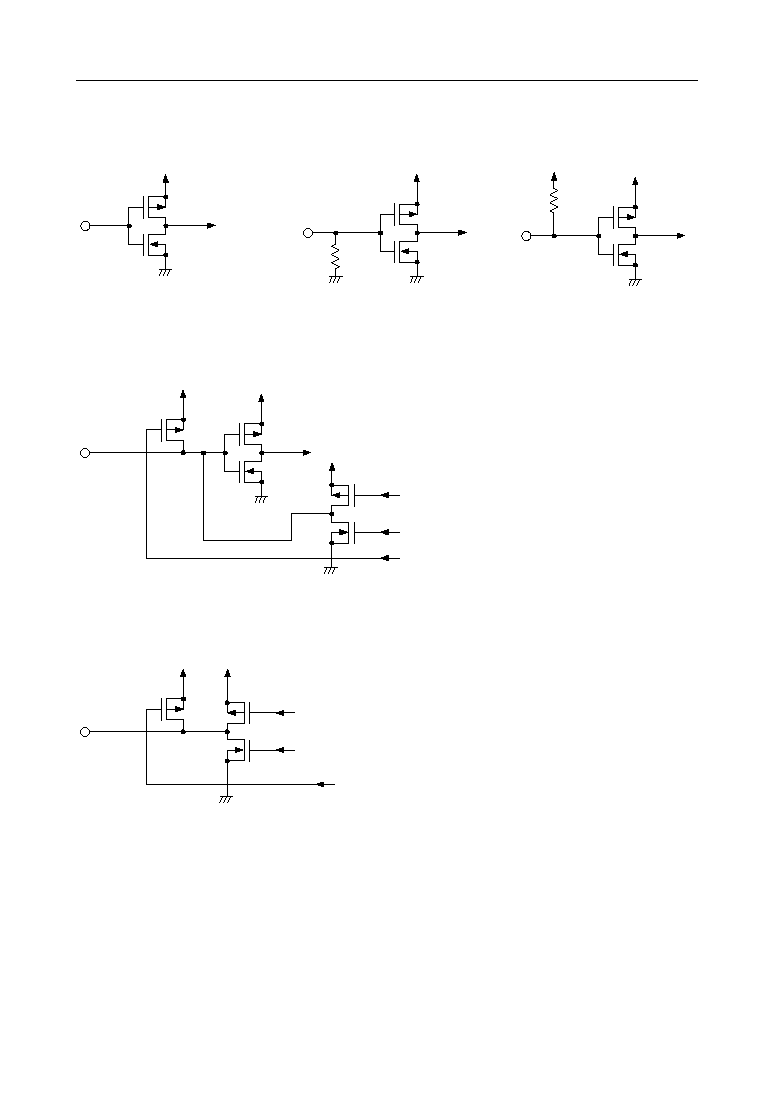
I/O CIRCUITS
V
DD
P
N
Applied to pins E, SSR, CSR, BEB, CS
P/S, SHT, and SI
V
DD
P
N
Applied to pins T
1
, T
2
, and T
3
V
DD
P
N
V
DD
Applied to pins R/W, RS
1
, and RS
0
V
DD
P
V
DD
P
N
V
DD
P
N
Applied to pins DB0 to DB7
Output Enable signal
V
DD
P P
V
DD
N
Applied to pins SO
Output Enable signal
Ў Semiconductor
ML9044
4/54
PIN DESCRIPTIONS
Symbol
Description
R/W
The input pin with a pullup resistor to select Read ("H") or Write ("L") in the Parallel
I/F Mode.
This pin should be open in the Serial I/F Mode.
RS
0
, RS
1
RS
1
RS
0
Name of register
H
H
Data register
H
L
Instruction register
L
L
Expansion Instruction register
The input pins with a pullup resistor to select a register in the Parallel I/F Mode.
This pin should be open in the Serial I/F Mode.
E
The input pin for data input/output between the CPU and the ML9044 and for activating
instructions in the Parallel I/F Mode.
This pin should be open in the Serial I/F Mode.
DB
0
to DB
3
The input/output pins to transfer data of lowerorder 4 bits between the CPU and the
ML9044 in the Parallel I/F Mode. Each pin is equipped with a pullup resistor. These 4
lines are not used for the 4bit interface.
This pin should be open in the Serial I/F Mode.
DB
4
to DB
7
The input/output pins to transfer data of upper 4 bits between the CPU and the ML9044
in the Parallel I/F Mode. Each pin is equipped with a pullup resistor.
This pin should be open in the Serial I/F Mode.
OSC
1
OSC
2
OSC
R
The clock oscillation pins required for LCD drive signals and the operation of the
ML9044 by instructions sent from the CPU.
To input external clock, the OSC
1
pin should be used. The OSC
R
and the OSC
2
pins
should be open.
To start oscillation with an external resistor, the resistor should be connected between
the OSC
1
and OSC
2
pins. The OSC
R
pin should be open.
To start oscillation with an internal resistor, the OSC
2
and OSC
R
pins should be
shortcircuited outside the ML9044. The OSC
1
pin should be open.
COM
1
to COM
17
The LCD common signal output pins.
For 1/9 duty, nonselectable voltage waveforms are output via COM
10
to COM
17
. For
1/12 duty, nonselectable voltage waveforms are output via COM
13
to COM
17
.
SEG
1
to SEG
120
The LCD segment signal output pins.

Ў Semiconductor
ML9044
5/54
SSR
The input pin to select the transfer direction of the segment signal output data.
"L": Data transfer from SEG
1
to SEG
120
"H": Data transfer from SEG
120
to SEG
1
V
1
, V
2
, V
3A
, V
3B
, V
4
The pins to output bias voltages to the LCD.
For 1/4 bias : The V
2
and V
3B
pins are shorted.
For 1/5 bias : The V
3A
and V
3B
pins are shorted.
BEB
The input pin to enable or disable the voltage multiplier circuit.
"L" disables the voltage multiplier circuit. "H" enables the voltage multiplier circuit.
The voltage multiplier circuit doubles the input voltage V
IN
and outputs it to the V
5IN
pin.
The voltage multiplier circuit can be used only when generating a level lower than GND.
V
IN
The pin to input voltage to the voltage multiplier.
V
5
, V
5IN
The pins to supply the LCD drive voltage.
The LCD drive voltage is supplied to the V
5
pin when the voltage multiplier is not used
(BEB = 0) and the internal contrast adjusting circuit is also not used. At this time, the
V
5IN
pin should be open.
The LCD drive voltage is supplied to the V
5IN
pin when the voltage multiplier is not used
(BEB = 0) but the internal contrast adjusting circuit is used. At this time, the V
5
pin
should be open.
When the voltage multiplier is used (BEB = 1), the V
5IN
and V
5
pins should be open (the
multiplied voltage is output to the V
5IN
pin). In this case, the internal contrast adjusting
circuit is used automatically.
V
C
The pin to connect the positive pin of the capacitor for the voltage multiplier.
V
CC
The pin to connect the negative pin of the capacitor used for the voltage multiplier.
CSR
The input pin to select the transfer direction of the common signal output data.
Refer to the Expansion Instruction Codes section about the AS bit.
CSR
duty
AS bit
shift direction
arbitrator's common pin
L
1/9
L
COM1 Ж COM9
COM9
L
1/9
H
COM2 Ж COM9, COM1
COM1
L
1/12
L
COM1 Ж COM12
COM12
L
1/12
H
COM2 Ж COM12, COM1
COM1
L
1/17
L
COM1 Ж COM17
COM17
L
1/17
H
COM2 Ж COM17, COM1
COM1
H
1/9
L
COM9 Ж COM1
COM1
H
1/9
H
COM8 Ж COM1, COM9
COM9
H
1/12
L
COM12 Ж COM1
COM1
H
1/12
H
COM11 Ж COM1, COM12
COM12
H
1/17
L
COM17 Ж COM1
COM1
H
1/17
H
COM16 Ж COM1, COM17
COM17
Symbol
Description

Ў Semiconductor
ML9044
6/54
P/S
The input pin to select the parallel or serial interface.
"L" selects the parallel interface.
"H" selects the serial interface.
CS
The pin to enable this IC in the serial I/F mode.
"L" enables this IC.
"H" disables this IC.
This pin should be open in the parallel I/F mode.
SHT
The pin to input shift clock in the serial I/F mode.
Data inputting to the SI pin is carried out synchronizing with the rising edge of this
clock signal.
Data outputting from the SO pin is carried out synchronizing with the falling edge of this
clock signal.
This pin should be open in the parallel I/F mode.
SI
The pin to input DATA in the serial I/F mode.
Data inputting to this pin is carried out synchronizing with the rising edge of the SHT
signal.
This pin should be open in the parallel I/F mode.
SO
The pin to output DATA in the serial I/F mode.
Data inputting to this pin is carried out synchronizing with the falling edge of the SHT
signal.
This pin should be open in the parallel I/F mode.
Symbol
Description
T
1
, T
2
, T
3
The input pins for test circuits (normally open). Equipped with a pulldown resistor.
V
DD
The power supply pin.
GND
The ground level input pin.
Ў Semiconductor
ML9044
7/54
ABSOLUTE MAXIMUM RATINGS
Note:
This voltage should be applied across V
DD
and V
5
. The following voltages are output
to the V
1
, V
2
, V
3A
(V
3B
) and V
4
pins:
· 1/4 bias
V
1
= {V
DD
(V
DD
V
5
)/4}
±
0.15V
V
2
= V
3B
= {V
DD
(V
DD
V
5
)/2}
±
0.15V
V
4
= {V
DD
3 Ґ (V
DD
V
5
)/4 }
±
0.15V
· 1/5 bias
V
1
= {V
DD
(V
DD
V
5
)/5}
±
0.15V
V
2
= {V
DD
2 Ґ (V
DD
V
5
)/5}
±
0.15V
V
3A
= V
3B
= {V
DD
3 Ґ (V
DD
V
5
)/5}
±
0.15V
V
4
= {V
DD
4 Ґ (V
DD
V
5
)/5}
±
0.15V
The voltages at the V
1
, V
2
, V
3A
(V
3B
), V
4
and V
5
pins should satisfy
V
DD
>V
1
>V
2
>V
3A
(V
3B
)>V
4
>V
5
.
(Higher Ё
Ж Lower)
* Do not apply shortcircuiting across output pins and across an output pin and an
input/output pin or the power supply pin in the output mode.
RECOMMENDED OPERATING CONDITIONS
Parameter
Symbol
Condition
Rating
Unit
Applicable pins
(GND = 0V)
Supply Voltage
V
DD
Ta = 25°C
0.3 to +6.5
V
V
DD
GND
LCD Driving Voltage
V
1
, V
2
, V
3
,
V
4
, V
5
Ta = 25°C
V
DD
7.5 to V
DD
+0.3
V
V
1
, V
4
, V
5
, V
5IN
,
V
2
, V
3A
, V
3B
Input Voltage
V
I
Ta = 25°C
0.3 to V
DD
+0.3
V
R/W, E, SHT, CSR,
P/S, SSR, SI, RS
0,
RS
1
, BEB, CS,
T
1
to T
3
, DB
0
to DB
7
,
V
IN
Storage Temperature
T
STG
--
55 to +125
°C
--
Parameter
Symbol
Condition
Range
Unit Applicable pins
(GND = 0V)
Supply Voltage
V
DD
--
2.5 to 5.5
V
V
DD
GND
Input Voltage
V
IN
BEB = 1
V
DD
1.40 to
V
DD
3.5
V
V
DD
V
IN
LCD Driving Voltage
V
DD
V
5
(See Note)
--
2.8 to 7.0
V
V
DD
V
5
(V
5IN
)
Operating Temperature
T
op
--
40 to +85
°C
--
Ў Semiconductor
ML9044
8/54
ELECTRICAL CHARACTERISTICS
DC Characteristics
(GND = 0V, V
DD
= 2.5V to 5.5V, Ta = 40 to +85°C)
Parameter
Symbol
Condition
Min
Typ
Max
Unit
Applicable pin
"H" Input Voltage 1
V
IH1
--
0.8V
DD
--
V
DD
V
"L" Input Voltage 1
V
IL1
0.3
--
0.2V
DD
"H" Input Voltage 2
V
IH2
--
0.8V
DD
--
V
DD
V
"L" Input Voltage 2
V
IL2
0.3
--
0.2V
DD
"H" Output Voltage 1 V
OH1
I
OH
= 0.1mA
0.75V
DD
--
--
V
"L" Output Voltage 1
V
OL1
I
OL
= +0.1mA
--
--
0.2V
DD
"H" Output Voltage 2 V
OH2
I
OH
= 13mA
0.9V
DD
--
--
V
"L" Output Voltage 2
V
OL2
I
OL
= +13mA
--
--
0.1V
DD
COM Voltage
Drop
V
CH
I
OCH
= 4mA
V
DD
0.3
V
DD
V
V
CMH
I
OCMH
= ±4mA
V
1
0.3
V
1
+ 0.3
V
CML
I
OCML
= ±4mA
V
4
0.3
V
4
+ 0.3
V
CL
I
OCL
= +4mA
V
5
V
5
+ 0.3
SEG Voltage
Drop
V
SH
I
OSH
= 4mA
V
DD
0.3
V
DD
V
V
SMH
I
OSMH
= ±4mA
V
2
0.3
V
2
+ 0.3
V
SML
I
OSML
= ±4mA
V
3
0.3
V
3
+ 0.3
V
SL
I
OSL
= +4mA
V
DD
V
5
= 5V
V
DD
V
5
= 5V
Note 1
Note 1
V
5
V
5
+ 0.3
Input Leakage
Current
| IIL |
V
DD
= 5V, V
IN
= 5V or 0V
--
--
1.0
m
A
Input Current 1
| II1|
V
DD
= 5V, V
IN
= GND
10
25
61
m
A
V
DD
= 5V, V
IN
= V
DD
,
Excluding current flowing
through the pull-up resistor
and the output driving MOS
--
--
2.0
Input Current 2
| II2|
V
DD
= 5V, V
IN
= V
DD
15
45
105
m
A
V
DD
= 5V, V
IN
= V
DD
,
Excluding current flowing
through the pull-down resistor
--
--
2.0
Supply Current
I
DD
V
DD
= 5V
Note 2
Rf = 120kW±2%
Note 3
OSC
1
: Open
OSC
2
and OSC
R
: Short-circuited
Note 4
OSC
2
, OSC
R
: Open
Input from OSC
1
--
--
1.2
mA
LCD Bias Resistor
R
LB
4.0
kW
Oscillation Frequency of
External Resistor Rf
f
osc1
175
270
350
kHz
Oscillation Frequency of
Internal Resistor Rf
f
osc2
140
270
480
kHz
Clock Input
Frequency
Input Clock Rise Time
External Clock
f
in
125
480
kHz
Input Clock Duty
f
duty
Note 5
45
50
55
%
f
rf
Note 6
--
--
0.2
m
S
f
ff
Note 6
--
--
0.2
m
S
E, SSR, CSR, BEB,
SHT, P/S, CS, SI
R/W, RS
0
, RS
1
DB
0
to DB
7
, SO
T
1
, T
2
, T
3
V
DD
GND
V
DD
, V
1
, V
2
V
3A
, V
3B
, V
4
, V
5
OSC
1
, OSC
2
OSC
1
, OSC
2
,
OSC
R
OSC
1
R/W, RS
0
, RS
1
,
E, DB
0
to DB
7
SHT, P/S, SI, CS
OSC
1
,
SSR, CSR, BEB
DB
0
to DB
7
, SO
OSC
2
COM
1
to COM
17
SEG
1
to SEG
120
Input Clock Fall Time
Ў Semiconductor
ML9044
9/54
Control Range of
LCD Driving
Voltage (by internal
variable resistor)
V
LCD
MAX
V
DD
= 5V, 1/5 bias
V
5IN
= 0V
TBD
--
V
LCD
MIN
V
DD
= 5V, 1/5 bias
V
5IN
= 0V
--
TBD
Bias Voltage for Driving
LCD by External Input
V
LCD1
V
DD
V5
2.8
--
7.0
V
V
LCD2
Note 7
1/5 bias
1/4 bias
2.8
--
7.0
Voltage Multiplier
Output Voltage
V5OUT V
DD
= 3V, V
IN
= 0V
BEB = H
V
DD
2V
IN
--
V
DD
2V
IN
+1.2V
V
Voltage Multipler
Input Voltage
V
IN
V
DD
/2
V
V
DD
V
5
V
5
V
5
, V
5IN
V
IN
(GND = 0V, V
DD
= 2.5V to 5.5V, Ta = 40 to +85°C)
Parameter
Symbol
Condition
Min
Typ
Max
Unit
Applicable pin

Ў Semiconductor
ML9044
10/54
Note 1:
Applied to the voltage drop occurring between any of the V
DD
, V
1
, V
4
and V
5
pins and
any of the common pins (COM
1
to COM
17
) when the current of 4mA flows in or flows
out at one common pin.
Also applied to the voltage drop occurring between any of the V
DD
, V
2
, V
3A
(V
3B
) and
V
5
pins and any of the segment pins (SEG
1
to SEG
120
) when the current of 4mA flows
in or flows out at one common pin.
The current of 4mA flows out when the output level is V
DD
or flows in when the output
level is V
5
.
Note 2:
Applied to the current flowing into the V
DD
pin when the external clock (f
osc2
= f
in
=
270 kHz) is fed to the internal R
f
oscillation or OSC
1
under the following conditions:
V
DD
= 5V
GND = V
5
= 0V,
V
1
, V
2
, V
3A
(V
3B
) and V
4
: Open
E, SSR, CSR, and BEB: "L" (fixed)
Other input pins: "L" or "H" (fixed)
Other output pins: No load
OSC
1
OSC
R
OSC
2
The wire between OSC
2
and OSC
R
should be as short
as possible. Keep OSC
1
open.
OSC
1
OSC
R
OSC
2
The wire between OSC
1
and R
f
and the wire between
OSC
2
and R
f
should be as short as possible.
Keep OSC
R
open.
R
f
= 120kW±2%
t
HW
t
LW
V
DD
2
f
IN
waveform
V
DD
2
V
DD
2
Applied to the pulses entering from the OSC
1
pin
f
duty
= t
HW
/ (t
HW
+ t
LW
) Ґ 100 (%)
Note 3:
Note 4:
Note 5:
Ў Semiconductor
ML9044
11/54
Note 7:
For 1/4 bias, V
2
and V
3B
pins are shortcircuited. V
3A
pin is open.
For 1/5 bias, V
3A
and V
3B
pins are shortcircuited. V
2
pin is open.
Note 6:
0.7V
DD
Applied to the pulses entering from the OSC
1
pin
0.7V
DD
0.3V
DD
0.3V
DD
t
rf
t
ff
Ў Semiconductor
ML9044
12/54
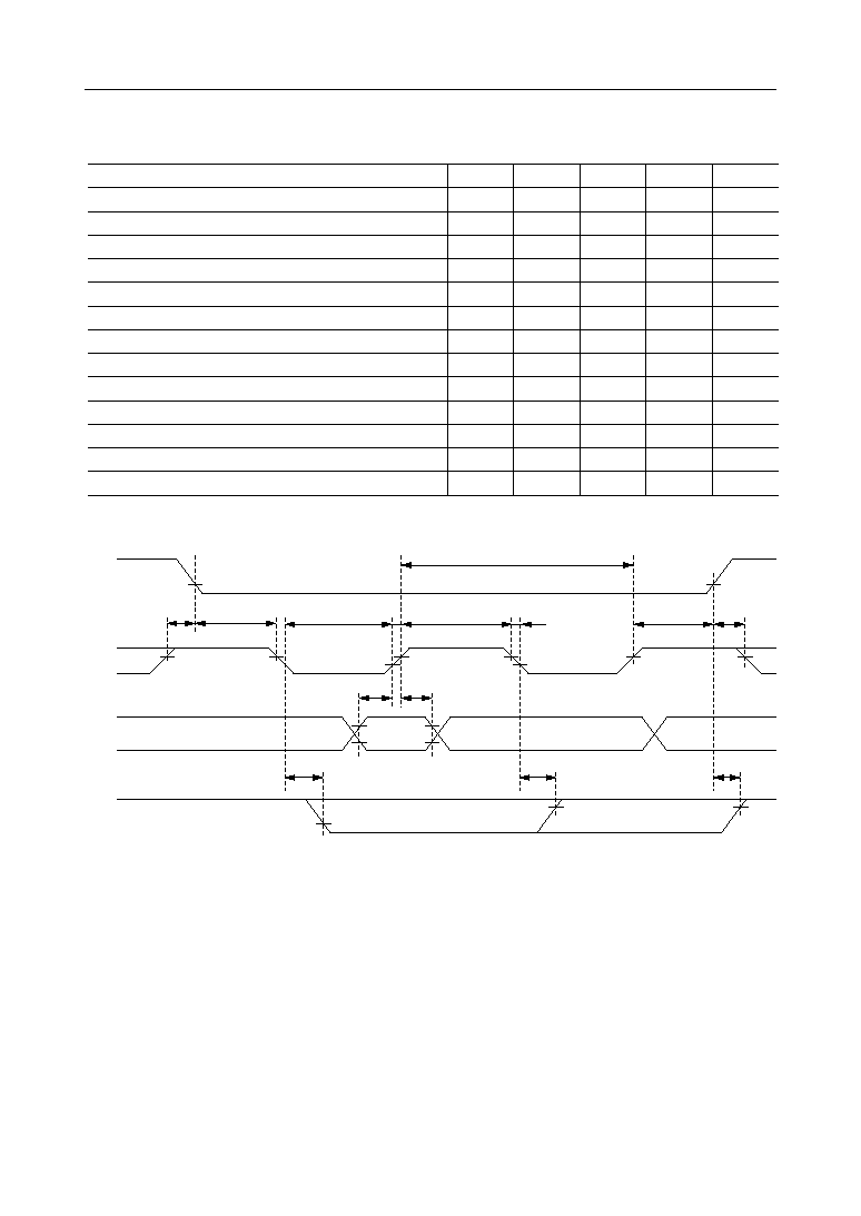
Switching Characteristics (The following ratings are subject to change after ES evaluation.)
· Parallel Interface Mode
The timing for the input from the CPU (see 1) and the timing for the output to the CPU (see 2)
are as shown below:
1) WRITE MODE (Timing for input from the CPU)
(V
DD
= 2.5 to 5.5V, Ta = 40 to +85°C)
Parameter
Symbol
Unit
Min
Typ
Max
R/W, RS
0
, RS
1
Setup time
40
--
--
t
B
ns
E Pulse Width
450
--
--
t
W
ns
R/W, RS
0
, RS
1
Hold time
10
--
--
t
A
ns
E Rise Time
--
--
25
t
r
ns
E Fall Time
--
--
25
t
f
ns
E Pulse Width
430
--
--
t
L
ns
E Cycle Time
1000
--
--
t
C
ns
DB
0
to DB
7
Input Data Hold time
195
--
--
t
I
ns
DB
0
to DB
7
Input Data Setup time
10
--
--
t
H
ns
RS
1
, RS
0
V
IH
V
IL
V
IH
V
IL
V
IL
V
IL
V
IL
V
IL
V
IL
V
IH
V
IH
V
IH
V
IL
V
IH
V
IL
R/W
E
DB
0
to DB
7
t
L
t
B
t
W
t
r
t
f
t
A
t
H
t
I
Input
Data
t
c
Ў Semiconductor
ML9044
13/54
2) READ MODE (Timing for output to the CPU)
(V
DD
= 2.5 to 5.5V, Ta = 40 to +85°C)
Parameter
Symbol
Unit
Min
Typ
Max
R/W, RS
1
, RS
0
Setup Time
40
--
--
t
B
ns
E Pulse Width
450
--
--
t
W
ns
R/W, RS
1
, RS
0
Hold Time
10
--
--
t
A
ns
E Rise Time
--
--
25
t
r
ns
E Fall Time
--
--
25
t
f
ns
E Pulse Width
430
--
--
t
L
ns
E Cycle Time
1000
--
--
t
C
ns
DB
0
to DB
7
Output Data Delay Time
--
--
350
t
D
ns
DB
0
to DB
7
Output Data Hold Time
20
--
--
t
O
ns
RS1, 0
V
IH
V
IL
V
IH
V
IL
V
IH
V
IH
V
IL
V
IL
V
IL
V
IH
V
IH
V
OH
V
OL
V
OH
V
OL
R/W
E
DB
0
to DB
7
t
L
t
B
t
W
t
r
t
f
t
A
t
O
t
D
Output
Data
tc
Ў Semiconductor
ML9044
14/54
· Serial Interface Mode
(V
DD
= 2.5 to 5.5V, Ta = 40 to +85°C)
Parameter
Symbol
Unit
Min
Typ
Max
SHT Cycle Time
500
--
--
t
SCY
ns
CS Setup Time
100
--
--
t
CSU
ns
CS Hold Time
100
--
--
t
CH
ns
SHT Setup Time
60
--
--
t
SSU
ns
SHT Hold Time
200
--
--
t
SH
ns
SHT "H" Pulse Width
200
--
--
t
SWH
ns
SHT "L" Pulse Width
200
--
--
t
SWL
ns
SHT Rise Time
--
--
50
t
SR
ns
SHT Fall Time
--
--
50
t
SF
ns
SI Setup Time
100
--
--
t
DISU
ns
SI Hold Time
100
--
--
t
DIH
ns
Data Output Delay Time
--
--
160
t
DOD
ns
Data Output Hold Time
0
--
--
t
CDH
ns
V
IH
V
IL
V
IH
V
IL
SI
V
IL
t
SCY
t
DOD
t
DOD
V
OL
V
OH
V
OH
t
CDH
CS
SO
SHT
t
CSU
t
SSU
t
SWL
t
SR
t
SWH
t
SF
t
SH
t
CH
V
IH
V
IL
V
IH
V
IH
V
IH
V
IL
t
DISU
t
DIH

Ў Semiconductor
ML9044
15/54
FUNCTIONAL DESCRIPTION
Instruction Register (IR), Data Register (DR), and Expansion Instruction Register (ER)
These registers are selected by setting the level of the Register Selection input pins RS
0
and RS
1
.
The DR is selected when both RS
0
and RS
1
are "H". The IR is selected when RS0 is "L" and RS
1
is "H". The ER is selected when both RS
0
and RS
1
are "L". (When RS
0
is "H" and RS
1
is "L", the
ML9044 is not selected.)
The IR stores an instruction code and the address code of the display data RAM (DDRAM) or the
character generator RAM (CGRAM).
The microcontroller (CPU) can write to the IR but cannot read from the IR.
The ER stores a contrast adjusting code and the address code of the arbitrator RAM (ABRAM).
The CPU can write to or read from the ER.
The DR stores data to be written in the DDRAM, ABRAM and CGRAM and also stores data read
from the DDRAM, AMRAM and CGRAM.
The data written in the DR by the CPU is automatically written in the DDRAM, ABRAM or
CGRAM.
When an address code is written in the IR or ER, the data of the specified address is automatically
transferred from the DDRAM, ABRAM or CGRAM to the DR. The data of the DDRAM, ABRAM
and CGRAM can be checked by allowing the CPU to read the data stored in the DR.
After the CPU writes data in the DR, the data of the next address in the DDRAM, ABRAM or
CGRAM is selected to be ready for the next writing by the CPU. Similarly, after the CPU reads
the data in the DR, the data of the next address in the DDRAM, ABRAM or CGRAM is set in the
DR to be ready for the next reading by the CPU.
Writing in or reading from these 3 registers is controlled by changing the status of the R/
W(Read/Write) pin.
Table 1 R/W pin status and register operation
Busy Flag (BF)
The status "1" of the Busy Flag (BF) indicates that the ML9044 is carrying out internal operation.
When the BF is "1", any new instruction is ignored.
When R/W = "H", RS
0
= "L" and RS
1
= "H", the data in the BF is output to the DB
7
.
New instructions should be input when the BF is "0".
When the BF is "1", the output code of the address counter (ADC) is undefined.
R/W
RS
0
RS
1
Operation
Writing in the IR
L
L
H
Reading the Busy flag (BF) and the address counter (ADC)
H
L
H
Writing in the DR
L
H
H
Reading from the DR
H
H
H
Writing in the ER
L
L
L
Reading the contrast code
H
L
L

Ў Semiconductor
ML9044
16/54
Address Counter (ADC)
The address counter provides a read/write address for the DDRAM, ABRAM or CGRAM and
also provides a cursor display address.
When an instruction code specifying DDRAM, ABRAM or CGRAM address setting is input to
the predefined register, the register selects the specified DDRAM, ABRAM or CGRAM and
transfers the address code to the ADC. The address data in the ADC is automatically incremented
(or decremented) by 1 after the display data is written in or read from the DDRAM, ABRAM or
CGRAM.
The data in the ADC is output to DB
0
to DB
6
when R/W = "H", RS
0
= "L", RS
1
= "H" and BF =
"0".
Timing Generator
The timing generator generates timing signals for the internal operation of the ML9044 activated
by the instruction sent from the CPU or for the operation of the internal circuits of the ML9041
such as DDRAM, ABRAM, CGRAM and CGROM. Timing signals are generated so that the
internal operation carried out for LCD displaying will not be interfered by the internal operation
initiated by accessing from the CPU. For example, when the CPU writes data in the DDRAM,
the display of the LCD not corresponding to the written data is not affected.
Ў Semiconductor
ML9044
17/54
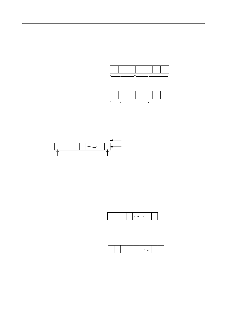
Display Data RAM (DDRAM)
This RAM stores the display data represented in 8bit character coding (see Table 2).
The DDRAM addresses correspond to the display positions (digits) of the LCD as shown below.
The DDRAM addresses (to be set in the ADC) are represented in hexadecimal.
MSB
LSB
DB
6
DB
5
DB
4
DB
3
DB
2
DB
1
DB
0
Hexadecimal
Hexadecimal
2
0
ADC
0
1
0
0
1
0
1
ADC
(Example) Representation of DDRAM address = 12
0 0 0 1 0 2 0 3 0 4
1 6 1 7
Digit
2
3
4
5
23 24
Left
end
Right
end
Display position
DD RAM address (hexadecimal)
1
4 F 0 0 0 1 0 2
1 5 1 6
Digit
2
3
4
23 24
(Display shifted to the right)
1
0 1 0 2 0 3 0 4
1 7 1 8
Digit
2
3
4
0 5
5
23 24
(Display shifted to the left)
1
1) Relationship between DDRAM addresses and display positions (1line display mode)
In the 1line display mode, the ML9044 can display up to 24 characters from digit 1 to digit 24.
While the DDRAM has addresses "00" to "4F" for up to 80 character codes, the area not used for
display can be used as a RAM area for general data. When the display is shifted by instruction,
the relationship between the LCD display and the DDRAM address changes as shown below:

Ў Semiconductor
ML9044
18/54
2) Relationship between DDRAM addresses and display positions (2line display mode)
In the 2line mode, the ML9044 can display up to 48 characters (24 characters per line) from digit
1 to digit 24.
0 0 0 1 0 2 0 3 0 4
Digit
2
3
4
5
1 6 1 7
23 24
4 0 4 1 4 2 4 3 4 4
5 6 5 7
Line 1
Line 2
Display position
DD RAM
address (hexadecimal)
1
2 7 0 0 0 1 0 2
1
2
3
4
1 5 1 6
23 24
6 7 4 0 4 1 4 2
5 5 5 6
Line 1
Line 2
0 1 0 2 0 3 0 4
1
2
3
4
1 7 1 8
23 24
4 1 4 2 4 3 4 4
0 3
5
4 3
0 5
5
4 5
5 7 5 8
Line 1
Line 2
(Display shifted to the right)
(Display shifted to the left)
Digit
Digit
Note:
The DDRAM address at digit 24 in the first line is not consecutive to the DDRAM address at digit
1 in the second line.
When the display is shifted by instruction, the relationship between the LCD display and the
DDRAM address changes as shown below:

Ў Semiconductor
ML9044
19/54
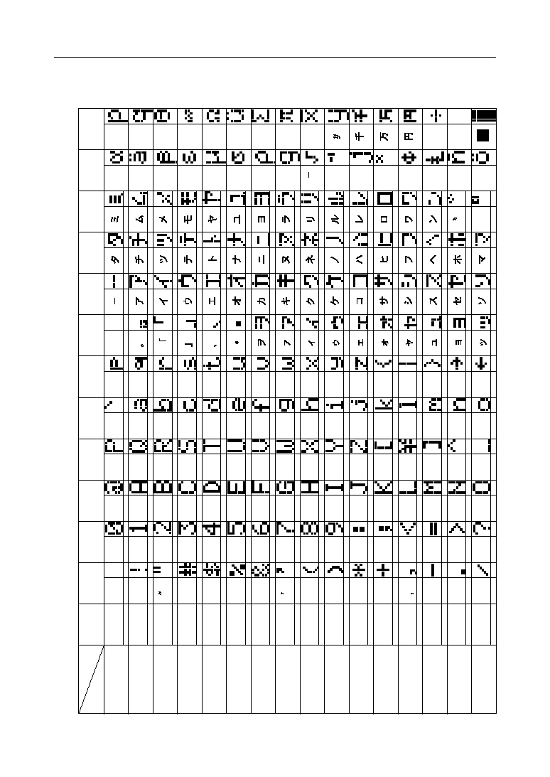
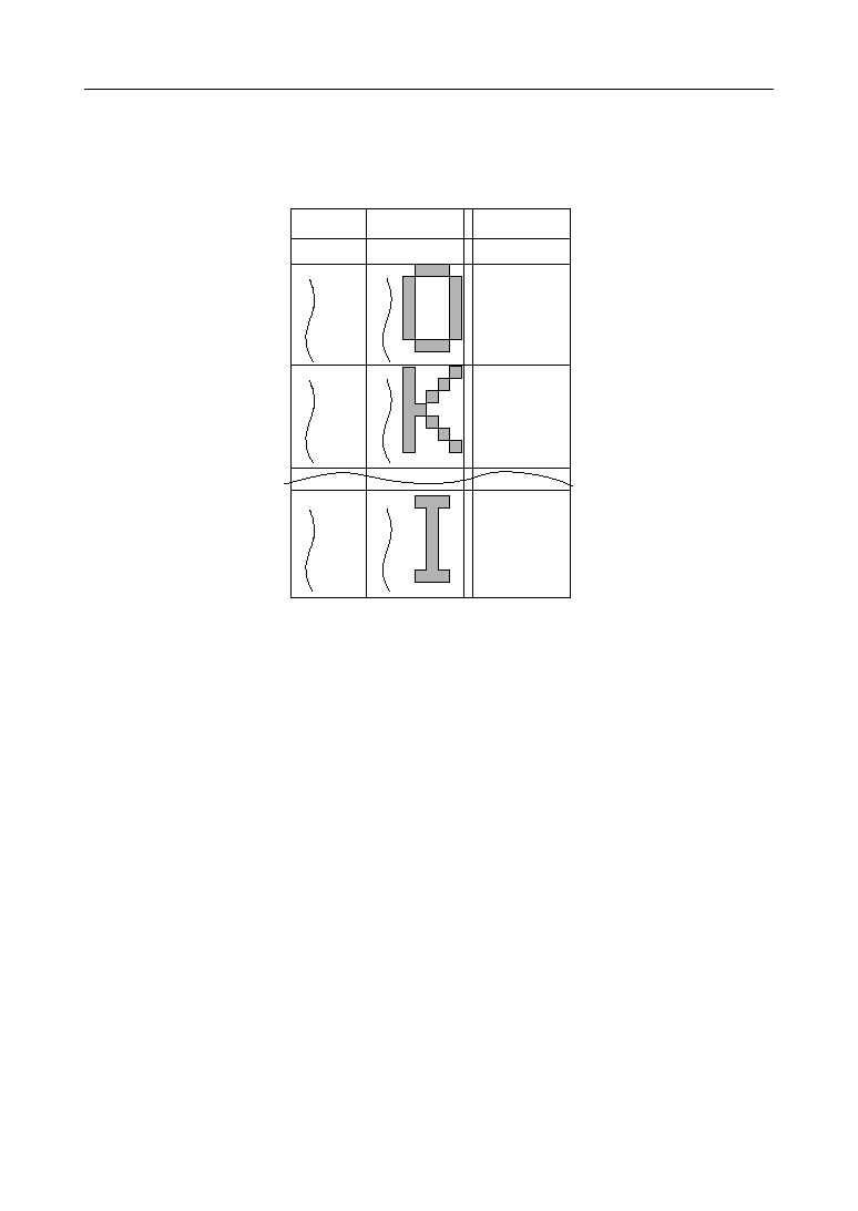
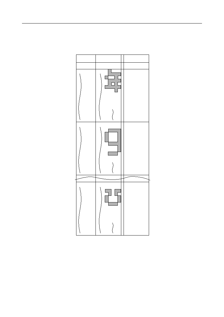
Character Generator ROM (CGROM)
The CGROM generates small character patterns (5 Ґ 7 dots, 160 patterns) or large character
patterns (5 Ґ 10 dots, 32 patterns) from the 8bit character code signals in the DDRAM. See Table
2 for the relationship between the 8bit character codes and the character patterns.
When the 8bit character code corresponding to a character pattern in the CGROM is written
in the DDRAM, the character pattern is displayed in the display position specified by the
DDRAM address.

Ў Semiconductor
ML9044
20/54
Character Generator RAM (CGRAM)
The CGRAM is used to generate userspecific character patterns that are not in the CGROM.
CGRAM (64 bytes = 512 bits) can store up to 8 small character patterns (5 Ґ 8 dots) or up to 4 large
character patterns (5 Ґ 11 dots).
When displaying a character pattern stored in the CGRAM, write an 8bit character code (00 to
07 or 08 to 0F; hex.) assigned in Table 2 to the DDRAM. This enables outputting the character
pattern to the LCD display position corresponding to the DDRAM address.
The cursor or blink is also displayed even when a CGRAM or ABRAM address is set in the ADC.
Therefore, the cursor or blink display should be inhibited while the ADC is holding a CGRAM
or ABRAM address.
The following describes how character patterns are written in and read from the CGRAM.
1) Small character patterns (5 Ґ 8 dots) (See Table 31.)
(1) A method of writing character patterns to the CGRAM from the CPU
The three CGRAM address bits 0 to 2 select one of the lines constituting a character pattern.
First, set the mode to increment or decrement from the CPU, and then input the CGRAM address.
Write each line of the character pattern code in the CGRAM through DB
0
to DB
7
.
The data lines DB0 to DB7 correspond to the CGRAM data bits 0 to 7, respectively (see Table 3.1).
Input data "1" represents the ON status of an LCD dot and "0" represents the OFF status. Since
the ADC is automatically incremented or decremented by 1 after the data is written to the
CGRAM, it is not necessary to set the CGRAM address again.
The bottom line of a character pattern (the CGRAM address bits 0 to 2 are all "1", which means
7 in hexadecimal) is the cursor line. The ON/OFF pattern of this line is ORed with the cursor
pattern for displaying on the LCD. Therefore, the pattern data for the cursor position should be
all zeros to display the cursor.
Whereas the data given by the CGRAM data bits 0 to 4 is output to the LCD as display data, the
data given by the CGRAM data bits 5 to 7 is not. Therefore, the CGRAM data bits 5 to 7 can be
used as a RAM area.
(2) A method of displaying CGRAM character patterns on the LCD
The CGRAM is selected when the higherorder 4 bits of a character code are all zeros. Since bit
3 of a character code is not used, the character pattern "0" in Table 31 can be selected using the
character code "00" or "08" in hexadecimal.
When the 8bit character code corresponding to a character pattern in the CGRAM is written to
the DDRAM, the character pattern is displayed in the display position specified by the DDRAM
address. (The DDRAM data bits 0 to 2 correspond to the CGRAM address bits 3 to 5,
respectively.)

Ў Semiconductor
ML9044
21/54
2) Large character patterns (5 Ґ 11 dots) (See Table 32.)
(1) A method of writing character patterns to the CGRAM from the CPU
The four CGRAM address bits 0 to 3 select one of the lines constituting a character pattern.
First, set the mode to increment or decrement from the CPU, and then input the CGRAM address.
Write each line of the character pattern code in the CGRAM through DB
0
to DB
7
.
The data lines DB
0
to DB
7
correspond to the CGRAM data bits 0 to 7, respectively (see Table 3
2). Input data "1" represents the ON status of an LCD dot and "0" represents the OFF status.
Since the ADC is automatically incremented or decremented by 1 after the data is written to the
CGRAM, it is not necessary to set the CGRAM address again.
The bottom line of a character pattern (the CGRAM address bits 0 to 3 are all "1", which means
A in hexadecimal) is a cursor line. The ON/OFF pattern of this line is ORed with the cursor
pattern for displaying on the LCD. Therefore, the pattern data for the cursor position should be
all zeros to display the cursor.
Whereas the data given by the CGRAM data bits 0 to 4 with the CGRAM addresses 0 to A in
hexadecimal (set by the CGRAM address bits 0 to 3) is output as display data to the LCD, the data
given by the CGRAM data bits 5 to 7 or the CGRAM addresses B to F in hexadecimal is not. These
bits can be written and read as a RAM area.
(2) A method of displaying CGRAM character patterns on the LCD
The CGRAM is selected when the higherorder 4 bits of a character code are all zeros. Since bits
0 and 3 of a character code are not used, the character pattern "b" in Table 32 can be selected with
a character code "00", "01", "08" or "09" in hexadecimal.
When the 8bit character code corresponding to a character pattern in the CGRAM is written to
the DDRAM, the character pattern is displayed in the display position specified by the DDRAM
address. (The DDRAM data bits 1 and 2 correspond to the CGRAM address bits 4 and 5,
respectively.)
Ў Semiconductor
ML9044
22/54
Arbitrator RAM (ABRAM)
The arbitrator RAM(ABRAM) stores arbitrator display data.
The ABRAM address is set at the ADC with the relationship illustrated below. Its valid address
area is 00 to 23 (00H to 17H).
Although an address exceeding 23 (17H) can be set or the address already set may exceed it due
to automatic increment or decrement processing, any address out of the valid address area is
ignored.
The cursor or blink is also displayed even when a CGRAM or ABRAM address is set in the ADC.
Therefore, the cursor or blink display should be inhibited while the ADC is hoding a CGRAM
or ABRAM address.
MSB
LSB
DB
6
DB
5
DB
4
DB
3
DB
2
DB
1
DB
0
Hexadecimal
Hexadecimal
ADC
*
*
E4
E3
E2
E1
E0
DB
6
*
DB
7
DB
5
DB
4
DB
3
DB
2
DB
1
DB
0
*
Don't Care
Display - ON data
E4
E4
5XSn+1
5XSn+5
Configuration of input display data
Input data
Relationship between display-ON
data and segment pins
Sn = ABRAM address (0 to 23)
The arbitrator RAM can store a maximum of 120 dots of the arbitrator DisplayON data in units
of 5 dots.
The arbitrator display is not shifted by any instructions and has the following relationship with
the LCD display positions:.
Ў Semiconductor
ML9044
23/54
Table 2 Relationship between character codes and character patterns of the ML9044
Lower
4 bits
Upper
4 bits
0000
LSB
0010
0011
0100
0101
0110
0111
1000
1001
1010
1011
1100
1101
1110
1111
MSB
0000
0010
0011
0100
0101
0110
0111
1010
1011
1100
1101
1110
1111
0001
CG
RAM (1)
(3)
(4)
(5)
(6)
(7)
(8)
(1)
(2)
(3)
(4)
(5)
(9)
(7)
(8)
(2)
#
$
%
&
(
)
*
+
.
/
!
2
3
4
5
6
7
8
9
:
;
<
=
>
?
1
0
B
C
D
E
F
G
H
I
J
K
L
M
N
O
A
@
R
S
T
U
V
W
X
Y
Z
[
Ґ
]
^
_
Q
P
b
c
d
e
f
n
h
i
j
k
l
m
n
o
a
/
r
s
t
u
v
w
x
y
z
{
Щ
}
Ж
Ё
q
p
°
b
e
m
s
r
g
1
j
x
ў
Ј
n
ц
д
a
Q
·
W
ь
S
p
X
ч
q
R
Ў Semiconductor
ML9044
24/54
Table 31
Relationship between CGRAM address bits, CGRAM data bits (character pattern)
and DDRAM data bits (character code) in 5 Ґ 7 dot character mode. (Examples)
CG RAM
CG RAM
address
(Character pattern)
(Character code)
data
DD RAM
data
5 4 3 2 1 0
0 0 0 0 0 0
0 0 1
0 1 0
0 1 1
1 0 0
1 0 1
1 1 0
1 1 1
0 1 1 1 0
1 0 0 0 1
1 0 0 0 1
1 0 0 0 1
1 0 0 0 1
1 0 0 0 1
0 1 1 1 0
0 0 0 0 0
7 6 5 4 3 2 1 0
7 6 5 4 3 2 1 0
MSB
LSB
MSB
LSB
MSB
LSB
0 0 0 0 Ґ 0 0 0
Ґ Ґ Ґ
0 0 1 0 0 0
0 0 1
0 1 0
0 1 1
1 0 0
1 0 1
1 1 0
1 1 1
1 0 0 0 1
1 0 0 1 0
1 0 1 0 0
1 1 0 0 0
1 0 1 0 0
1 0 0 1 0
1 0 0 0 1
0 0 0 0 0
0 0 0 0 Ґ 0 0 1
Ґ Ґ Ґ
1 1 1 0 0 0
0 0 1
0 1 0
0 1 1
1 0 0
1 0 1
1 1 0
1 1 1
0 1 1 1 0
0 0 1 0 0
0 0 1 0 0
0 0 1 0 0
0 0 1 0 0
0 0 1 0 0
0 1 1 1 0
0 0 0 0 0
0 0 0 0 Ґ 1 1 1
Ґ Ґ Ґ
Ґ
: Don't Care
Ў Semiconductor
ML9044
25/54
Table 32
Relationship between CGRAM address bits, CGRAM data bits (character pattern)
and DDRAM data bits (character code) in 5 Ґ 10 dot character mode (Examples)
CG RAM
CG RAM
address
(Character pattern)
(Character code)
data
DD RAM
data
5 4 3 2 1 0
7 6 5 4 3 2 1 0
7 6 5 4 3 2 1 0
LSB
MSB
MSB
LSB
MSB
LSB
0 0 0 0 Ґ 0 0 Ґ
Ґ Ґ Ґ
0 0 0 0 0 0
0 0 0 1
0 0 1 0
0 0 1 1
0 1 0 0
0 1 0 1
0 1 1 0
0 1 1 1
1 0 0 0
1 0 0 1
1 0 1 0
1 0 1 1
1 1 0 0
1 1 0 1
1 1 1 0
1 1 1 1
0 0 0 0 Ґ 0 0 Ґ
Ґ Ґ Ґ
0 0 0 0 0 0
0 0 0 1
0 0 1 0
0 0 1 1
0 1 0 0
0 1 0 1
0 1 1 0
0 1 1 1
1 0 0 0
1 0 0 1
1 0 1 0
1 0 1 1
1 1 0 0
1 1 0 1
1 1 1 0
1 1 1 1
0 0 0 0 0
0 0 0 0 0
0 1 1 1 1
1 0 0 0 1
1 0 0 0 1
1 0 0 0 1
0 1 1 1 1
0 0 0 0 1
0 0 0 0 1
0 1 1 1 0
0 0 0 0 0
Ґ Ґ Ґ Ґ Ґ
0 0 0 0 Ґ 1 1 Ґ
Ґ Ґ Ґ
0 0 0 0 0 0
0 0 0 1
0 0 1 0
0 0 1 1
0 1 0 0
0 1 0 1
0 1 1 0
0 1 1 1
1 0 0 0
1 0 0 1
1 0 1 0
1 0 1 1
1 1 0 0
1 1 0 1
1 1 1 0
1 1 1 1
0 0 0 0 0
0 0 0 0 0
1 1 0 1 1
0 1 0 1 0
1 0 0 0 1
1 0 0 0 1
0 1 1 1 0
0 0 0 0 0
0 0 0 0 0
0 0 0 0 0
0 0 0 0 0
Ґ Ґ Ґ Ґ Ґ
Ґ
: Don't Care
0
0 1 0 0 0
0 1 1 1 1
1 0 0 1 0
0 1 1 1 1
0 1
1 1 1 1 1
0 0 0 1 0
0 0 0 0 0
0 0 0 0 0
0 0 0 0 0
0 0 0 0 0
Ґ Ґ Ґ Ґ Ґ
0
1

Ў Semiconductor
ML9044
26/54
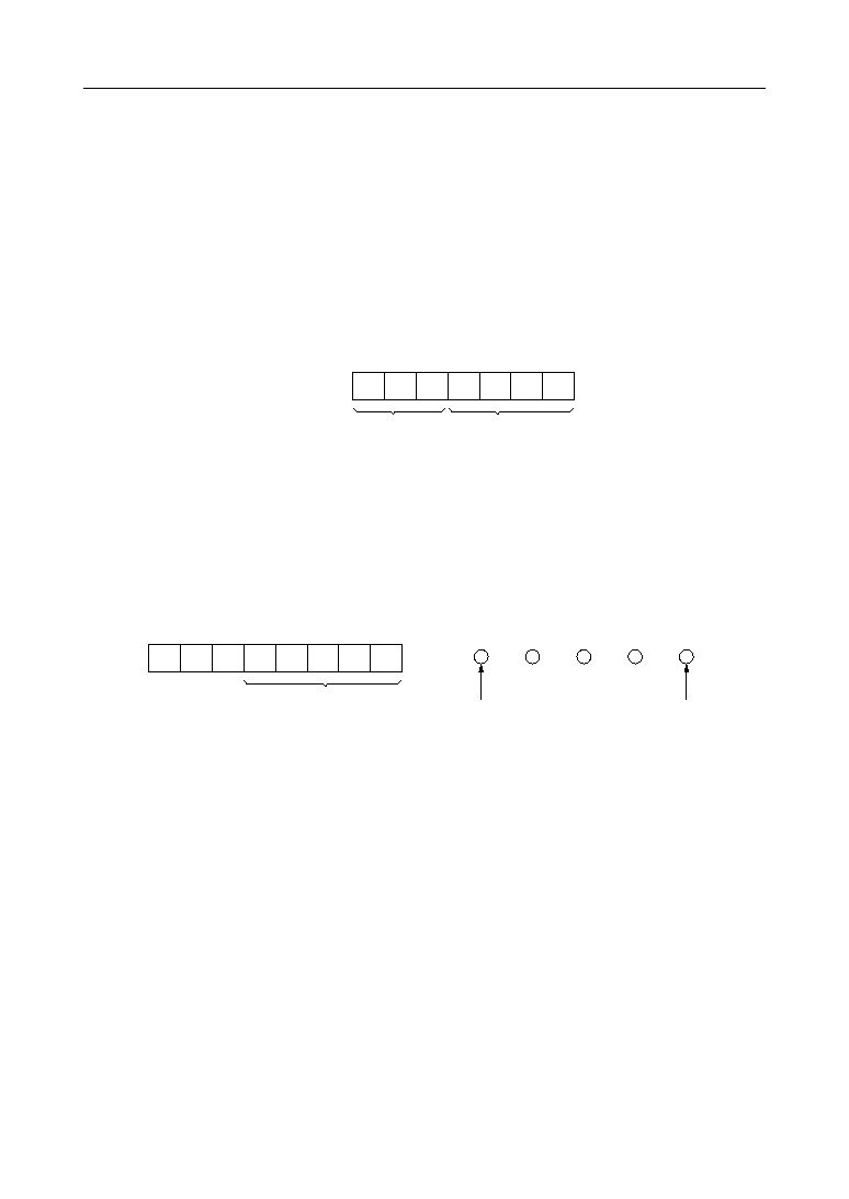
Cursor/Blink Control Circuit
This circuit generates the cursor and blink of the LCD.
The operation of this circuit is controlled by the program of the CPU.
The cursor/blink display is carried out in the position corresponding to the DDRAM address set
in the ADC (Address Counter).
For example, when the ADC stores a value of "07" (hexadecimal), the cursor or blink is displayed
as follows:
Note:
The cursor or blink is also displayed even when a CGRAM or ABRAM address is set
in the ADC. Therefore, the cursor or blink display should be inhibited while the ADC
is holding a CGRAM or ABRAM address.
0
DB6
DB0
0 0
0
1
1
1
7
0
0 0 0 1 0 2 0 3 0 4
0 7 0 8
1
2
3
4
5
8
9
Cursor/blink position
1 6 1 7
23 24
6
7
0 5 0 6
0 0 0 1 0 2 0 3 0 4
0 7 0 8
1
2
3
4
5
8
9
Cursor/blink position
1 6 1 7
23 24
6
7
0 5 0 6
4 0 4 1 4 2 4 3 4 4
4 7 4 8
5 6 5 7
4 5 4 6
First line
ADC
In 1-line display mode
In 2-line display mode
Second line
Digit
Digit

Ў Semiconductor
ML9044
27/54
LCD Display Circuit (COM1 to COM17, SEG1 to SEG120, SSR and CSR)
The ML9044 has 17 common signal outputs and 120 segment signal outputs to display 24
characters (in the 1line display mode) or 48 characters (in the 2line display mode).
The character pattern is converted into serial data and transferred in series through the shift
register.
The transfer direction of serial data is determined by the SSR pin. The shift direction of common
signals is determined by the CSR pin. The following tables show the transfer and shift directions:
* Refer to the Expansion Instruction Codes section about the AS bit.
Signals to be input to the SSR and CSR pins should be determined at poweron and be kept
unchanged.
CSR
duty
AS bit
Shift direction
arbitrator's common pin
L
1/9
L
COM1 Ж COM9
COM9
L
1/9
H
COM2 Ж COM9, COM1
COM1
L
1/12
L
COM1 Ж COM12
COM12
L
1/12
H
COM2 Ж COM12, COM1
COM1
L
1/17
L
COM1 Ж COM17
COM17
L
1/17
H
COM2 Ж COM17, COM1
COM1
H
1/9
L
COM9 Ж COM1
COM1
H
1/9
H
COM8 Ж COM1, COM9
COM9
H
1/12
L
COM12 Ж COM1
COM1
H
1/12
H
COM11 Ж COM1, COM12
COM12
H
1/17
L
COM17 Ж COM1
COM1
H
1/17
H
COM16 Ж COM1, COM17
COM17
SSR
Transfer direction
L
SEG
1
Ж
SEG
120
H
SEG
120
Ж
SEG
1
Ў Semiconductor
ML9044
28/54
Builtin Reset Circuit
The ML9044 is automatically initialized when the power is turned on.
During initialization, the Busy Flag (BF) is "1" and the ML9041 does not accept any instruction
from the CPU (other than the Read BF instruction).
The Busy Flag is "1" for about 15 ms after the V
DD
becomes 2.5 V or higher.
During this initialization, the ML9044 performs the following instructions:
1)
Display clearing
2)
CPU interface data length = 8 bits
(DL = "1")
3)
1line LCD display
(N = "0")
4)
Font size = 5 Ґ 7 dots
(F = "0")
5)
ADC counting = Increment
(I/D = "1")
6)
Display shifting = None
(S = "0")
7)
Display = Off
(D = "0")
8)
Cursor = Off
(C = "0")
9)
Blinking = Off
(B = "0")
10) Arbitrator = Displayed in the lower line
(AS = "0")
11) Setting 1FH (hexadecimal) to the Contrast Data
To use the builtin reset circuit, the power supply conditions shown below should be satisfied.
Otherwise, the builtin reset circuit may not work properly. In such a case, initialize the ML9044
with the instructions from the CPU. The use of a battery always requires such initialization from
the CPU. (See "Initial Setting of Instructions")
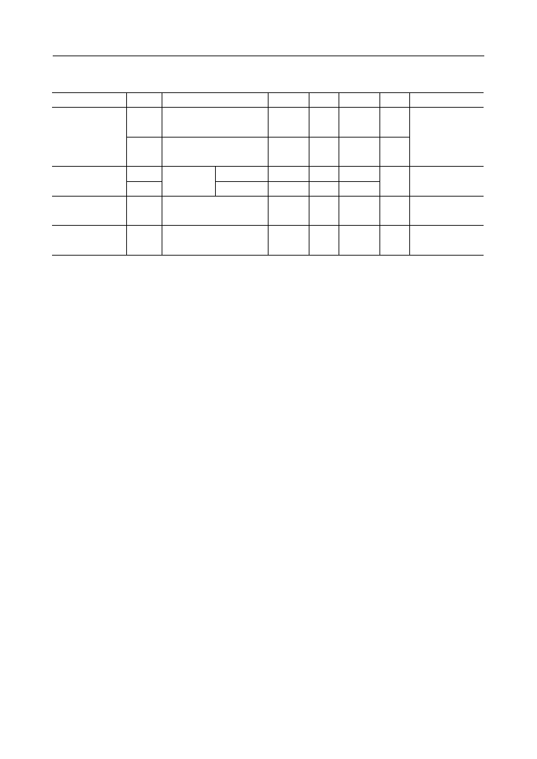
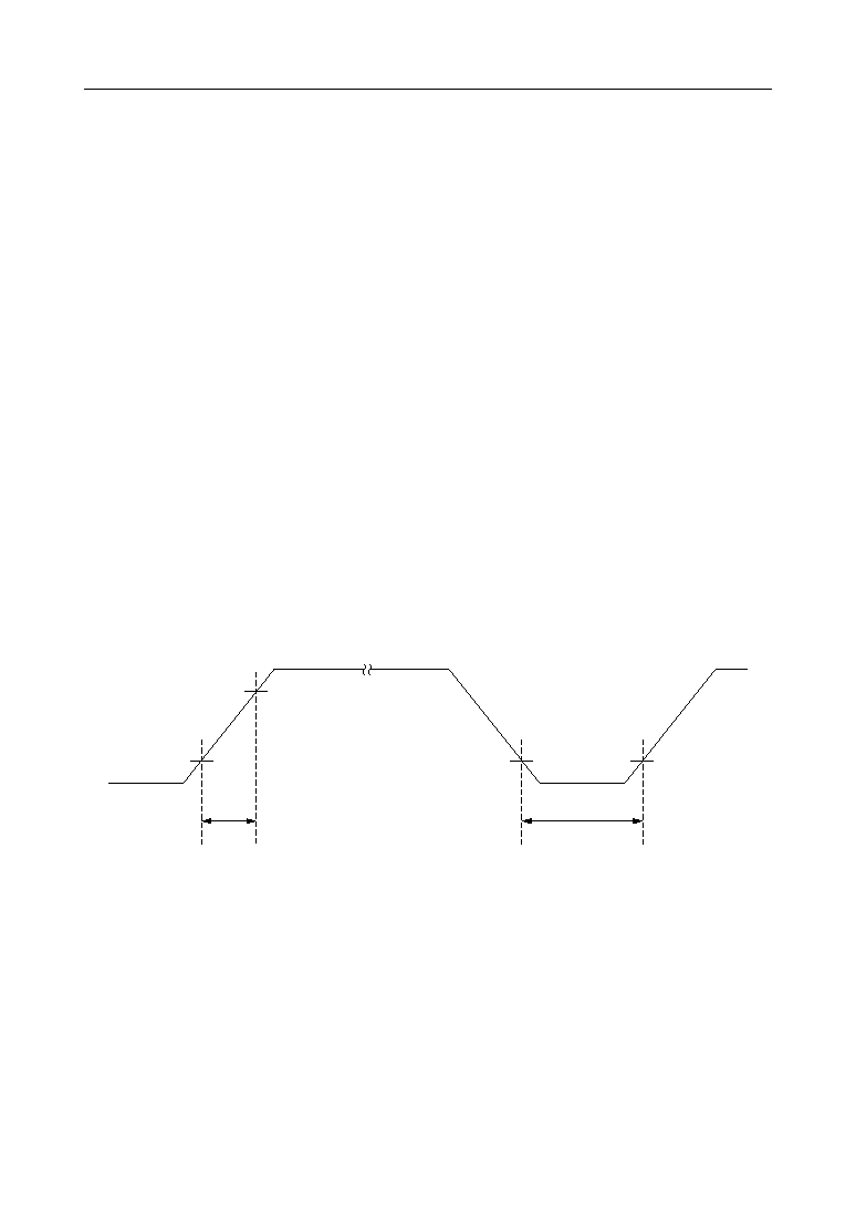
Figure 1 Poweron and Poweroff Waveform
t
ON
2.5V
0.2V
0.2V
0.2V
t
OFF
0.1msЈ t
ON
Ј
100ms
1msЈ t
OFF

Ў Semiconductor
ML9044
29/54
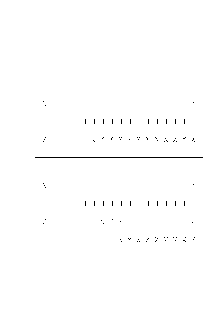
I/F with CPU
Parallel interface mode
The ML9044 can transfer either 8 bits once or 4 bits twice on the data bus for interfacing with any
8bit or 4bit microcontroller (CPU).
1) 8bit interface data length
The ML9044 uses all of the 8 data bus lines DB0 to DB7 at a time to transfer data to and from the
CPU.
2) 4bit interface data length
The ML9044 uses only the higherorder 4 data bus lines DB
4
to DB
7
twice to transfer 8bit data
to and from the CPU.
The ML9044 first transfers the higherorder 4 bits of 8bit data (DB
4
to DB
7
in the case of 8bit
interface data length) and then the lowerorder 4 bits of the data (DB
0
to DB
3
in the case of 8bit
interface data length).
The lowerorder 4 bits of data should always be transferred even when only the transfer of the
higherorder 4 bits of data is required. (Example: Reading the Busy Flag)
Two transfers of 4 bits of data complete the transfer of a set of 8bit data. Therefore, when only
one access is made, the following data transfer cannot be completed properly.
Ў Semiconductor
ML9044
30/54
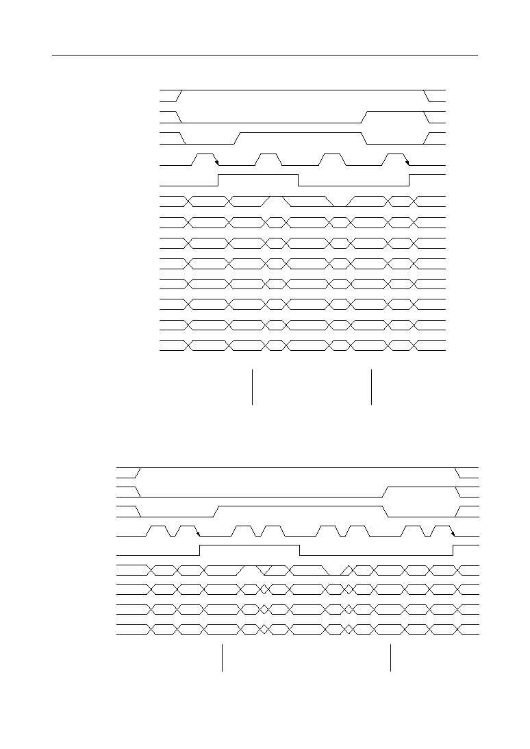
Figure 2 8-Bit Data Transfer
Figure 3 4-Bit Data Transfer
RS
0
R/W
E
Busy
(Internal operation)
IR
7
DB
6
DB
5
DB
4
DB
3
DB
2
DB
1
DB
0
DB
7
Busy
No
Busy
DR
7
IR
6
DR
6
ADC
6
IR
5
DR
5
ADC
5
IR
4
DR
4
ADC
4
IR
3
DR
3
ADC
3
IR
2
DR
2
ADC
2
IR
1
DR
1
ADC
1
IR
0
DR
0
ADC
0
RS
1
Writing In IR
(Instruction
Register)
Reading BF (Busy Flag)
and ADC (Address Counter)
Writing In DR
(Data Register)
RS
0
R/W
E
Busy
(Internal operation)
DB
7
DB
6
DB
5
DB
4
IR
7
Busy
No
Busy
DR
7
DR
3
ADC
3
ADC
5
DR
6
DR
2
ADC
2
DR
5
DR
1
ADC
1
ADC
4
DR
4
DR
0
ADC
0
ADC
6
IR
3
IR
6
IR
2
IR
5
IR
1
IR
4
IR
0
RS
1
Writing In IR
(Instruction
Register)
Reading BF (Busy Flag)
and ADC (Address Counter)
Writing In DR
(Data Register)
Ў Semiconductor
ML9044
31/54
Serial Interface Mode
In the Serial I/F Mode, the ML9044 interfaces with the CPU via the CS, SHT, SI and SO pins.
Writing and reading operations are executed in units of 16 bits after the CS signal falls down. If
the CS signal rises up before the completion of 16bit unit access, this access is ignored.
When the BF bit is "1", the ML9044 cannot accept any other instructions. Before inputting a new
instruction, check that the BF bit is "0". Any access when the BF bit is "1" is ignored.
Data format is LSBfirst.
Examples of Access in the Serial I/F Mode
1) WRITE MODE
CS
SO
SHT
SI
1
2
3
4
5
1
1
1
1
1
6
7
8
9
10
11
12
13
14
15
16
D
7
D
6
D
5
D
4
D
3
D
2
D
1
D
0
RS
1
RS
0
R/W
CS
SO
SHT
SI
1
2
3
4
5
1
1
1
1
1
6
7
8
9
10
11
12
13
14
15
16
RS
1
RS
0
R/W
D
7
D
6
D
5
D
4
D
3
D
2
D
1
D
0
2) READ MODE
Ў Semiconductor
ML9044
32/54
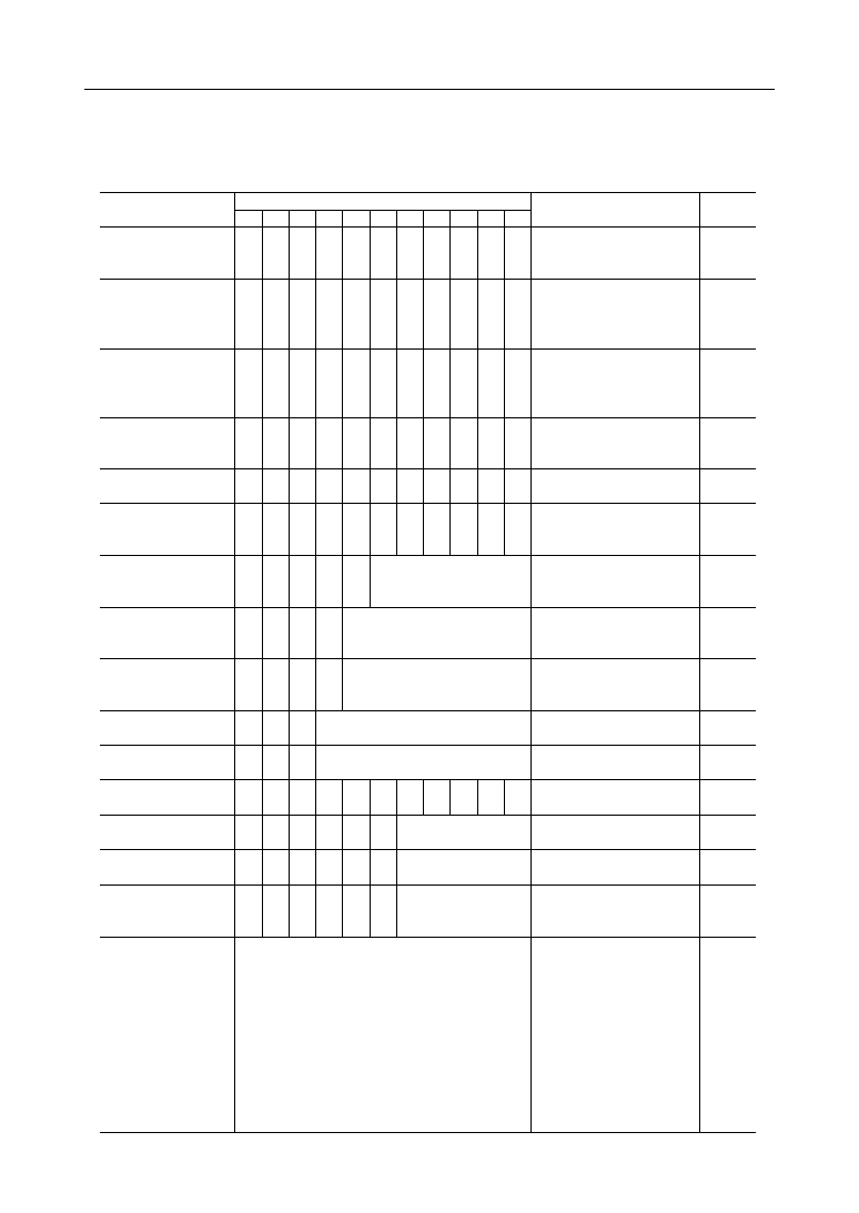
Instruction Codes
Table of Instruction Codes
Display Clear
Cursor Home
Entry Mode Setting
Displya ON/OFF Control
Cursor/Display Shift
Function Setting
CGRAM Address Setting
DDRAM Address Setting
Busy Flag/Address Read
RAM Data Write
RAM Data Read
Contrast Control Data Write
Contrast Control Data Read
Instruction
Function
Execution
Time
f = 270kHz
Code
DB0
DB1
DB2
DB3
DB4
DB5
DB6
DB7
R/W
RS0
RS1
Clears all the displayed digits of the LCD and
sets the DDRAM address 0 in the address
counter. The arbitrator data is cleared.
Sets the DDRAM address 0 in the address
counter and shifts the display back to the
original. The content of the DDRAM
remains unchanged.
Determines the direction of movement of
the cursor and whether or not to shift the
display. This instruction is executed when
data is written or read.
Sets LCD display ON/OFF (D), cursor
ON/OFF or cursor-position character
blinking ON/OFF.
Moves the cursor or shifts the display
without changing the content of the DDRAM.
Sets the interface data length (DL), the
number of display lines (N) or the type of
character font (F).
Sets on CGRAM address. After that,
CGRAM data is transferred to and from
the CPU.
Sets a DDRAM address. After that DDRAM
data is transferred to and from the CPU.
Reads the Busy Flag (indicating that the
ML9044 is operating) and the content of
the address counter.
Writes data in DDRAM, ABRAM or CGRAM.
Reads data from DDRAM, ABRAM or CGRAM.
Writes data to control the contrast of the LCD.
Reads data to control the contrast of the LCD.
The
execution
time is
dependent
upon
frequencies
DD RAM
CG RAM
ABRAM
ACG
ADD
AAB
ADC
: Display data RAM
: Character generator RAM
: Arbitrator data RAM
: CGRAM address
: DDRAM address (Corresponds to
the cursor address)
: ABRAM address
: Address counter (Used by DDRAM,
ABRAM and CGRAM)
I/D = "0"
S/C = "0"
R/L = "0"
DL = "0"
N = "0"
F = "0"
BF = "0"
AS = "0"
I/D = "1"
S = "1"
S/C = "1"
R/L = "1"
D/L = "1"
N = "1"
F = "1"
BF = "1"
B = "1"
C = "1"
D = "1"
AS = "1"
(Decrement)
(Moves the cursor.)
(Left shift)
(4-bit data)
(1 line)
(5 Ґ 7 dots)
(Ready to accept
an instruction)
(Arbitrator Displays
arbitrator on the lower line)
(Increment)
(Shifts the display.)
(Shifts display.)
(Right shift)
(8-bit data)
(2 lines)
(5 Ґ 10 dots)
(Busy)
(Enables blinking.)
(Displyas the corsor.)
(Displays a character pattern.)
(Arbitrator Displays arbitrator
on the upper line)
1.52 ms
1.52 ms
37 ms
37 ms
37 ms
37 ms
37 ms
37 ms
0 ms
37 ms
37 ms
37 ms
37 ms
1
0
0
0
0
0
0
0
0
0
1
*
1
0
0
0
0
0
0
0
0
1
S
I/D
1
0
0
0
0
0
0
0
1
B
C
D
1
0
0
0
0
0
0
1
*
*
R/L
S/C
1
0
0
0
0
0
1
*
*
F
N
DL
1
0
0
0
0
1
1
0
0
0
1
1
0
0
1
BF
1
0
1
0
1
1
1
1
1
0
0
0
1
0
0
1
0
0
0
0
0
ACG
ADD
ADC
WRITE DATA
READ DATA
Arbitrator Display Line Set
Sets the arbitrator display line.
37 ms
0
0
0
0
0
0
0
1
AS
0
0
WRITE (Contrast Data) DATA
READ (Contrast Data) DATA
ABRAM address setting
Sets an ABRAM address. After that
ABRAM data is transferred to and from
the CPU.
37 ms
0
0
0
1
1
0
AAB
--
Ґ: Don't Care
Ў Semiconductor
ML9044
33/54
Instruction Codes
An instruction code is a signal sent from the CPU to access the ML9044. The ML9044 starts
operation as instructed by the code received. The busy status of the ML9044 is rather longer than
the cycle time of the CPU, since the internal processing of the ML9044 starts at a timing which
does not affect the display on the LCD. In the busy status (Busy Flag is "1"), the ML9044 executes
the Busy Flag Read instruction only. Therefore, the CPU should ensure that the Busy Flag is "0"
before sending an instruction code to the ML9044.
1) Display Clear
When this instruction is executed, the LCD display including arbitrator display is cleared and the
I/D entry mode is set to "Increment". The value of "S" (Display shifting) remains unchanged.
The position of the cursor or blink being displayed moves to the left end of the LCD (or the left
end of the line 1 in the 2line display mode).
Note:
All DDRAM and ABRAM data turn to "20" and "00" in hexadecimal, respectively. The
value of the address counter (ADC) turns to the one corresponding to the address "00"
(hexadecimal) of the DDRAM.
The execution time of this instruction is 1.52 ms (maximum) at an oscillation frequency
of 270 kHz.
2) Cursor Home
When this instruction is executed, the cursor or blink position moves to the left end of the LCD
(or the left end of line 1 in the 2line display mode). If the display has been shifted, the display
returns to the original display position before shifting.
Note:
The value of the address counter (ADC) goes to the one corresponding to the address
"00" (hexadecimal) of the DDRAM).
The execution time of this instruction is 1.52 ms (maximum) at an oscillation frequency
of 270 kHz.
RS
1
1
RS
0
0
R/W
0
DB
7
0
DB
6
0
DB
5
0
DB
4
0
DB
3
0
DB
2
0
DB
1
0
DB
0
1
Instruction Code :
RS
1
1
RS
0
0
R/W
0
DB
7
0
DB
6
0
DB
5
0
DB
4
0
DB
3
0
DB
2
0
DB
1
1
DB
0
Ґ
Instruction code:
Ґ
: Don't Care
Ў Semiconductor
ML9044
34/54
3) Entry Mode Setting
(1) When the I/D is set, the cursor or blink shifts to the right by 1 character position (ID= "1";
increment) or to the left by 1 character position (I/D= "0"; decrement) after an 8bit character
code is written to or read from the DDRAM. At the same time, the address counter (ADC) is also
incremented by 1 (when I/D = "1"; increment) or decremented by 1 (when I/D = "0"; decrement).
After a character pattern code is written to or read from the CGRAM, the address counter (ADC)
is incremented by 1 (when I/D = "1"; increment) or decremented by 1 (when I/D = "0";
decrement).
Also after data is written to or read from the ABRAM, the address counter (ADC) is incremented
by 1 (when I/D = "1"; increment) or decremented by 1 (when I/D = "0"; decrement).
(2) When S = "1", the cursor or blink stops and the entire display shifts to the left (I/D = "1") or
to the right (I/D = "0") by 1 character position after a character code is written to the DDRAM.
In the case of S = "1",when a character code is read from the DDRAM, when a character pattern
data is written to or read from the CGRAM or when data is written to or read from the ABRAM,
normal read/write is carried out without shifting of the entire display. (The entire display does
not shift, but the cursor or blink shifts to the right (I/D = "1") or to the left (I/D = "0") by 1
character position.)
When S = "0", the display does not shift, but normal write/read is performed.
Note:
The execution time of this instruction is 37 ms (maximum) at an oscillation frequency
of 270 kHz.
4) Display Mode Setting
(1) The "D" bit (DB2) of this instruction determines whether or not to display character patterns
on the LCD.
When the "D" bit is "1", character patterns are displayed on the LCD.
When the "D" bit is "0", character patterns are not displayed on the LCD and the cursor/blink
setting is also canceled.
Note:
Unlike the Display Clear instruction, this instruction does not change the character
code in the DDRAM and ABRAM.
(2 ) When the "C" bit (DB1) is "0", the cursor turns off. When both the "C" and "D" bits are "1",
the cursor turns on.
(3) When the "B" bit (DB0) is "0", blinking is canceled. When both the "B" and "D" bits are "1",
blinking is performed.
In the Blinking mode, all dots including those of the cursor, the character pattern and the cursor
are alternately displayed.
Note:
The execution time of this instruction is 37 ms (maximum) at an oscillation frequency
of 270kHz.
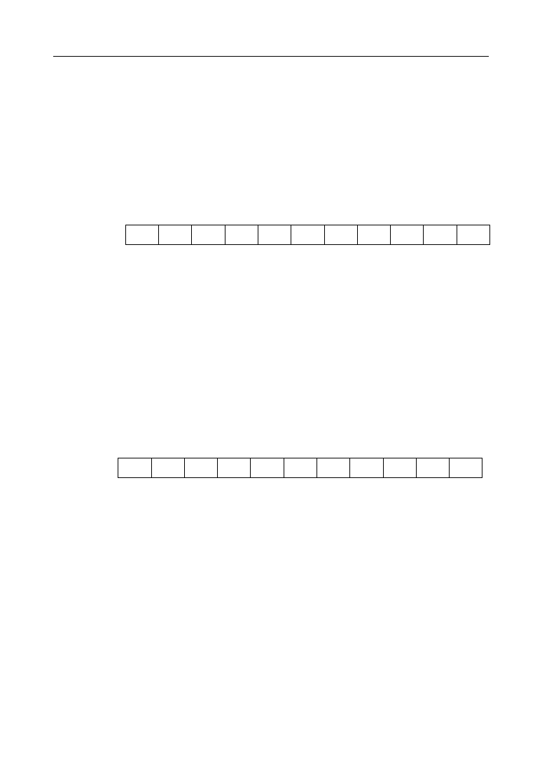
RS
1
1
RS
0
0
R/W
0
DB
7
0
DB
6
0
DB
5
0
DB
4
0
DB
3
0
DB
2
1
DB
1
I/D
DB
0
S
Instruction code:
RS
1
1
RS
0
0
R/W
0
DB
7
0
DB
6
0
DB
5
0
DB
4
0
DB
3
1
DB
2
D
DB
1
C
DB
0
B
Instruction code:

Ў Semiconductor
ML9044
35/54
5) Cursor/Display Shift
S/C = "0", R/L = "0" This instruction shifts left the cursor and blink positions by 1 (decrements
the content of the ADC by 1).
S/C = "0", R/L = "1" This instruction shifts right the cursor and blink positions by 1 (increments
the content of the ADC by 1).
S/C = "1", R/L = "0" This instruction shifts left the entire display by 1 character position. The
cursor and blink positions move to the left together with the entire display.
The Arbitrator display is not shifted.
(The content of the ADC remains unchanged.)
S/C = "1", R/L = "1" This instruction shifts right the entire display by 1 character position. The
cursor and blink positions move to the right together with the entire display.
The Arbitrator display is not shifted.
(The content of the ADC remains unchanged.)
In the 2line mode, the cursor or blink moves from the first line to the second line when the cursor
at digit 40 (27; hex) of the first line is shifted right.
When the entire display is shifted, the character pattern, cursor or blink will not move between
the lines (from line 1 to line 2 or vice versa).
Note:
The execution time of this instruction is 37 ms at an oscillation frequency (OSC) of 270
kHz.
6) Function Setting
(1) When the "DL" bit (DB4) of this instruction is "1", the data transfer to and from the CPU is
performed once by the use of 8 bits DB
7
to DB
0
.
When the "DL" bit (DB4) of this instruction is "0", the data transfer to and from the CPU is
performed twice by the use of 4 bits DB
7
to DB
4
.
(2) The 2line display mode is selected when the "N" bit (DB3) of this instruction is "1". The 1
line display mode is selected when the "N" bit is "0".
(3) The character font represented by 5 Ґ 7 dots is selected when the "F" bit (DB2) of this
instruction is "1". The character font represented by 5 Ґ 10 dots is selected when the "F" bit is "1"
and the "N" bit is "0".
After the ML9044 is powered on, this initial setting should be carried out before execution of any
instruction except the Busy Flag Read. After this initial setting, no instructions other than the DL
Set instruction can be executed. In the Serial I/F Mode, DL setting is ignored.
Note:
The execution time of this instruction is 37 ms at an oscillation frequency (OSC) of 270
kHz.
RS
1
1
RS
0
0
R/W
0
DB
7
0
DB
6
0
DB
5
0
DB
4
1
DB
3
S/C
DB
2
R/L
DB
1
Ґ
DB
0
Ґ
Instruction code:
Ґ
: FDon't Care
RS
1
1
RS
0
0
R/W
0
DB
7
0
DB
6
0
DB
5
1
DB
4
DL
DB
3
N
DB
2
F
DB
1
Ґ
DB
0
Ґ
Ґ
: Don't Care
Instruction code:
N
F
Number of
display lines
Font size
Duty
Number of
biases
Number of
common signals
0
0
1
5Ґ7
1/9
4
9
0
1
1
5Ґ10
1/12
4
12
1
0
2
5Ґ7
1/17
5
17
1
1
2
5Ґ7
1/17
5
17
Ў Semiconductor
ML9044
36/54
7) CGRAM Address Setting
RS
1
1
RS
0
0
R/W
0
DB
7
0
DB
6
1
DB
5
C
5
DB
4
C
4
DB
3
C
3
DB
2
C
2
DB
1
C
1
DB
0
C
0
Instruction code:
RS
1
1
RS
0
0
R/W
0
DB
7
1
DB
6
D
6
DB
5
D
5
DB
4
D
4
DB
3
D
3
DB
2
D
2
DB
1
D
1
DB
0
D
0
Instruction code:
RS
1
1
RS
0
1
R/W
0
DB
7
E
7
DB
6
E
6
DB
5
E
5
DB
4
E
4
DB
3
E
3
DB
2
E
2
DB
1
E
1
DB
0
E
0
Instruction code:
This instruction sets the character data corresponding to the CGRAM address represented by the
bits C5 to C0 (binary).
The CGRAM addresses are valid until DDRAM or ABRAM addresses are set.
The CPU writes or reads character patterns starting from the one represented by the CGRAM
address bits C
5
to C
0
set in the instruction code at that time.
Note:
The execution time of this instruction is 37 ms at an oscillation frequency (OSC) of 270
kHz.
8) DDRAM Address Setting
This instruction sets the character data corresponding to the DDRAM address represented by the
bits D6 to D0 (binary).
The DDRAM addresses are valid until CGRAM or ABRAM addresses are set.
The CPU writes or reads character patterns starting from the one represented by the DDRAM
address bits D6 to D0 set in the instruction code at that time.
In the 1line mode (the "N" bit is "1"), the DDRAM address represented by bits D6 to D0 (binary)
should be in the range "00" to "4F" in hexadecimal.
In the 2line mode (the "N" bit is "2"), the DDRAM address represented by bits D6 to D0 (binary)
should be in the range "00" to "27" or "40" to "67" in hexadecimal.
If an address other than above is input, the ML9044 cannot properly write a character code in or
read it from the DDRAM.
Note:
The execution time of this instruction is 37 ms at an oscillation frequency (OSC) of 270
kHz.
9) DDRAM/ABRAM/CGRAM Data Write
This instruction writes data represented by bits E
7
to E
0
(binary) to DDRAM, ABRAM or
CGRAM.
After data is written, the cursor, blink or display shifts according to the Cursor/Display Shift
instruction (see 5)).
Note:
The execution time of this instruction is 37 ms at an oscillation frequency (OSC) of 270
kHz.

Ў Semiconductor
ML9044
37/54
10) Busy Flag/Address Counter Read (Execution time: 1 ms)
The "BF" bit (DB7) of this instruction tells whether the ML9044 is busy in internal operation (BF
= "1") or not (BF = "0").
When the "BF" bit is "1", the ML9044 cannot accept any other instructions. Before inputting a
new instruction, check that the "BF" bit is "0".
When the "BF" bit is "0", the ML9044 outputs the correct value of the address counter. The value
of the address counter is equal to the DDRAM, ABRAM or CGRAM address. Which of the
DDRAM, ABRAM and CGRAM addresses is set in the counter is determined by the preceding
address setting.
When the "BF" bit is "1", the value of the address counter is not always correct because it may
have been incremented or decremented by 1 during internal operation.
11) DDRAM/ABRAM/CGRAM Data Read
A character code (P
7
to P
0
) is read from the DDRAM, DisplayON data (P
7
to P
0
) from the
ABRAM or a character pattern (P
7
to P
0
) from the CGRAM.
The DDRAM, ABRAM or CGRAM is selected at the preceding address setting.
After data is read, the address counter (ADC) is incremented or decremented as set by the
Transfer Mode Setting instruction (see 3).
Note:
Conditions for reading correct data
(1) The DDRAM, ABRAM or CGRAM Setting instruction is input before this data read
instruction is input.
(2) When reading a character code from the DDRAM, the Cursor/Display Shift instruction (see
5) is input before this Data Read instruction is input.
(3) When two or more consecutive RAM Data Read instructions are executed, the following read
data is correct.
Correct data is not output under conditions other than the cases (1), (2) and (3) above.
Note:
The execution time of this instruction is 37 ms at an oscillation frequency (OSC) of 270
kHz.
RS
1
1
RS
0
0
R/W
1
DB
7
BF
DB
6
O
6
DB
5
O
5
DB
4
O
4
DB
3
O
3
DB
2
O
2
DB
1
O
1
DB
0
O
0
Instruction code:
RS
1
1
RS
0
1
R/W
1
DB
7
P
7
DB
6
P
6
DB
5
P
5
DB
4
P
4
DB
3
P
3
DB
2
P
2
DB
1
P
1
DB
0
P
0
Instruction code:
Ў Semiconductor
ML9044
38/54
Expansion Instruction Codes
The busy status of the ML9044 is rather longer than the cycle time of the CPU, since the internal
processing of the ML9044 starts at a timing which does not affect the display on the LCD. In the
busy status (Busy Flag is "1"), the ML9041 executes the Busy Flag Read instruction only.
Therefore, the CPU should ensure that the Busy Flag is "0" before sending an expansion
instruction code to the ML9044.
1) Arbitrator Display Line Set
This expansion instruction code sets the Arbitrator display line. The relationship between the
status of this bit and the common outputs is as follows:
2) Contrast Adjusting Data Write
RS
1
0
RS
0
0
R/W
0
DB
7
0
DB
6
0
DB
5
0
DB
4
0
DB
3
0
DB
2
0
DB
1
1
DB
0
AS
Exparsion Instruction codes:
RS
1
0
RS
0
0
R/W
0
DB
7
0
DB
6
0
DB
5
1
DB
4
F
4
DB
3
F
3
DB
2
F
2
DB
1
F
1
DB
0
F
0
Exparsion Instraction codes:
CSR
duty
AS bit
Shift direction
Arbitrator's comon pin
L
1/9
L
COM1 Ж COM9
COM9
L
1/9
H
COM2 Ж COM9, COM1
COM1
L
1/12
L
COM1 Ж COM12
COM12
L
1/12
H
COM2 Ж COM12, COM1
COM1
L
1/17
L
COM1 Ж COM17
COM17
L
1/17
H
COM2 Ж COM17, COM1
COM1
H
1/9
L
COM9 Ж COM1
COM1
H
1/9
H
COM8 Ж COM1, COM9
COM9
H
1/12
L
COM12 Ж COM1
COM1
H
1/12
H
COM11 Ж COM1, COM12
COM12
H
1/17
L
COM17 Ж COM1
COM1
H
1/17
H
COM16 Ж COM1, COM17
COM17
This instruction writes contrast adjusting data (F
4
to F
0
) to the contrast register.
After contrast adjusting data is written in the register, the potential (VLCD) output to the V
5
pin
varies according to the data written.
The VLCD becomes maximum when the content of the contrast register is "1F" (hexadecimal)
and becomes minimum when it is "00" (hexadecimal).
Note:
The execution time of this instruction is 37 ms at an oscillation frequency (OSC) of 270
kHz.
Ў Semiconductor
ML9044
39/54
3) Contrast Adjusting Data Read
This instruction reads contrast adjusting data (G
4
to G
0
) from the contrast register.
Note:
The execution time of this instruction is 37 ms at an oscillation frequency (OSC) of 270
kHz.
4) ABRAM Address Setting
This instruction sets the character data corresponding to the ABRAM address represented by the
bits H
4
to H
0
(binary).
The ABRAM addresses are valid until CGRAM or DDRAM addresses are set.
The CPU writes or reads character patterns starting from the one represented by the ABRAM
address bits H
4
to H
0
set in the instruction code at that time.
The ABRAM address represented by bits H4 to H0 (binary) should be in the range "00" to "13"
in hexadecimal.
If an address other than above is input, the ML9044 cannot properly write a character code in or
read it from the DDRAM.
Note:
The execution time of this instruction is 37 ms at an oscillation frequency (OSC) of 270
kHz.
RS
1
0
RS
0
0
R/W
1
DB
7
0
DB
6
0
DB
5
0
DB
4
G
4
DB
3
G
3
DB
2
G
2
DB
1
G
1
DB
0
G
0
Exparsion Instruction code:
RS
1
0
RS
0
0
R/W
1
DB
7
0
DB
6
1
DB
5
1
DB
4
H
4
DB
3
H
3
DB
2
H
2
DB
1
H
1
DB
0
H
0
Exparsion Instruction code:

Ў Semiconductor
ML9044
40/54
LCD Drive Waveforms
The COM and SEG waveforms (AC signal waveforms for display) vary according to the duty (1/
9, 1/12 and 1/17 duties). See 1) to 3) below.
The relationship between the duty ratio and the frame frequency is as follows:
Note:
At an oscillation frequency (OSC) of 270 kHz
(1) Driving the LCD of one 24character line (1/9 duty, CSR = L, AS = 0) under the conditions
of the 1line display mode and the character font of 5 Ґ 7 dots
· COM
10
to COM
17
output DisplayOFF common signals.
Duty ratio
Frame Frequency
1/9
75.0Hz
1/12
56.3Hz
1/17
79.4Hz
COM
1
Character
Cursor
Arbitrator
COM
8
COM
9
SEG
1
SEG
120
ML9044

Ў Semiconductor
ML9044
41/54
(2) Driving the LCD of one 24character line (1/12 duty, CSR = L, AS = 0) under the conditions
of the 1line display mode and the character font of 5 Ґ 10 dots
· COM
13
to COM
17
output DisplayOFF common signals.
(3) Driving the LCD of two 24character line (1/17 duty, CSR = L, AS = 0) under the conditions
of the 2line display mode and the character font of 5 Ґ 7 dots
COM
1
COM
11
COM
12
SEG
1
SEG
120
MSM9044
Character
Cursor
Arbitrator
COM
1
COM
8
SEG
1
SEG
120
MSM9044
COM
9
COM
16
COM
17
Character
Cursor
Character
Cursor
Arbitrator
Ў Semiconductor
ML9044
42/54
EXAMPLES OF VLCD GENERATION CIRCUITS
· With 1/4bias, a builtin contrast adjusting circuit and a voltage multiplier
· With 1/5 bias, a builtin contrast adjusting circuit and the V5 level input from an external
circuit
ML9044
BEB
V
IN
V
CC
V
C
V
5IN
V
5
V
4
V
3B
V
3A
V
2
V
1
V
DD
Reference potential for
voltage multiplien
ML9044
BEB
V
IN
V
CC
V
C
V
5IN
V
5
V
4
V
3B
V
3A
V
2
V
1
V
DD
V
5
level

Ў Semiconductor
ML9044
43/54
1) COM and SEG Waveforms on 1/9 Duty
V
DD
8
1 frame
V
1
V
2
, V
3B
V
4
V
5
V
DD
V
1
V
2
, V
3B
V
4
V
5
V
DD
V
1
V
2
, V
3B
V
4
V
5
V
DD
V
1
V
2
, V
3B
V
4
V
5
COM
1
(CSR = L, AS = L)
COM
2
(CSR = L, AS = H)
COM
9
(CSR = H, AS = L)
COM
8
(CSR = H, AS = H)
(first character line)
COM
2
(CSR = L, AS = L)
COM
3
(CSR = L, AS = H)
COM
8
(CSR = H, AS = L)
COM
7
(CSR = H, AS = H)
(second character line)
COM
8
(CSR = L, AS = L)
COM
9
(CSR = L, AS = H)
COM
2
(CSR = H, AS = L)
COM
1
(CSR = H, AS = H)
(cursor line)
COM
9
(CSR = L, AS = L)
COM
1
(CSR = L, AS = H)
COM
1
(CSR = H, AS = L)
COM
9
(CSR = H, AS = H)
(arbitrator line)
9 1 2 3 4
7 8 9 1 2 3 4
7 8 9 1 2
V
DD
V
1
V
2
, V
3B
V
4
V
5
COM
10
to
COM
17
V
DD
V
1
V
2
, V
3B
V
4
V
5
SEG
Display
turning-off
waveform
Display
turning-on
waveform
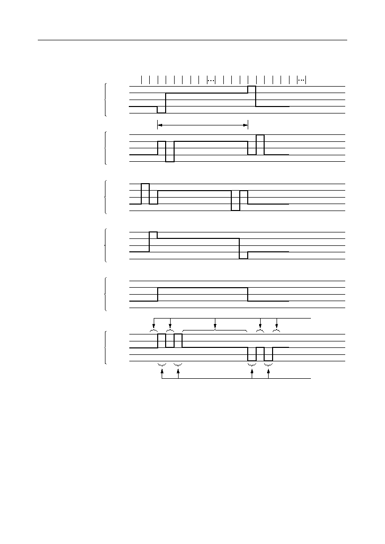
Ў Semiconductor
ML9044
44/54
2) COM and SEG Waveforms on 1/12 Duty
V
DD
1 frame
V
1
V
2
, V
3B
V
4
V
5
V
DD
V
1
V
2
, V
3B
V
4
V
5
V
DD
V
1
V
2
, V
3B
V
4
V
5
V
DD
V
1
V
2
, V
3B
V
4
V
5
V
DD
V
1
V
2
, V
3B
V
4
V
5
V
DD
V
1
V
2
, V
3B
V
4
V
5
Display
turning-off
waveform
Display
turning-on
waveform
11
COM
1
(CSR = L, AS = L)
COM
2
(CSR = L, AS = H)
COM
12
(CSR = H, AS = L)
COM
11
(CSR = H, AS = H)
(first character line)
COM
2
(CSR = L, AS = L)
COM
3
(CSR = L, AS = H)
COM
11
(CSR = H, AS = L)
COM
10
(CSR = H, AS = H)
(second character line)
COM
11
(CSR = L, AS = L)
COM
12
(CSR = L, AS = H)
COM
2
(CSR = H, AS = L)
COM
1
(CSR = H, AS = H)
(cursor line)
COM
12
(CSR = L, AS = L)
COM
1
(CSR = L, AS = H)
COM
1
(CSR = H, AS = L)
COM
12
(CSR = H, AS = H)
(arbitrator line)
12 1 2 3 4 5 6
9 10 11 12 1 2 3 4 5 6
COM
13
to
COM
17
SEG
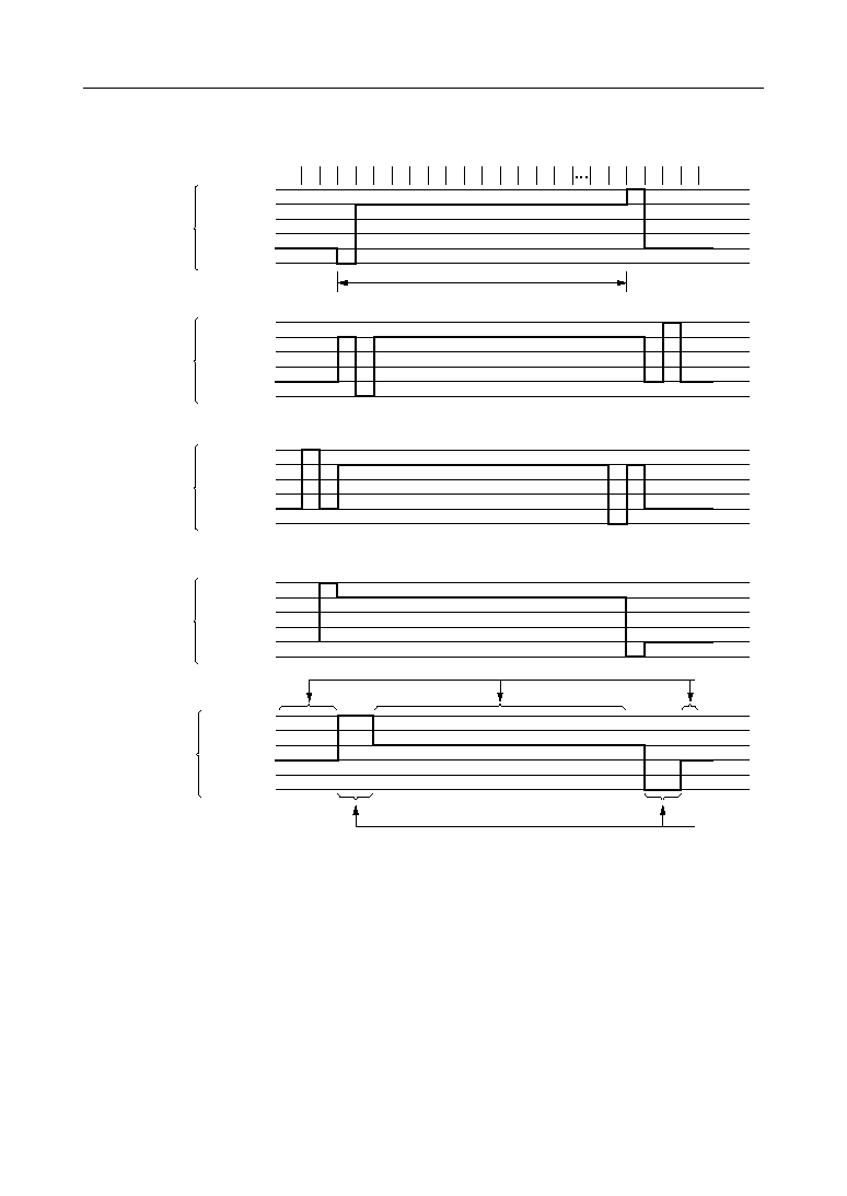
Ў Semiconductor
ML9044
45/54
3) COM and SEG Waveforms on 1/17 Duty
V
DD
16
1 frame
V
1
V
2
V
3A
(
V
3B
)
V
4
17 1 2 3 4 5 6 7 8 9 10 11 12 13
16 17 1 2
Display
turning-off
waveform
Display
turning-on
waveform
3 4
V
5
V
DD
V
1
V
2
V
3A
(
V
3B
)
V
4
V
5
V
DD
V
1
V
2
V
3A
(
V
3B
)
V
4
V
5
V
DD
V
1
V
2
V
3A
(
V
3B
)
V
4
SEG
V
5
V
DD
V
1
V
2
V
3A
(
V
3B
)
V
4
V
5
COM
1
(CSR = L, AS = L)
COM
2
(CSR = L, AS = H)
COM
17
(CSR = H, AS = L)
COM
16
(CSR = H, AS = H)
(first character line)
COM
2
(CSR = L, AS = L)
COM
3
(CSR = L, AS = H)
COM
16
(CSR = H, AS = L)
COM
15
(CSR = H, AS = H)
(second character line)
COM
16
(CSR = L, AS = L)
COM
17
(CSR = L, AS = H)
COM
2
(CSR = H, AS = L)
COM
1
(CSR = H, AS = H)
(corsor line)
COM
17
(CSR = L, AS = L)
COM
1
(CSR = L, AS = H)
COM
1
(CSR = H, AS = L)
COM
17
(CSR = H, AS = H)
(arbitrator line)

Ў Semiconductor
ML9044
46/54
Initial Setting of Instructions
(a) Data transfer from and to the CPU using 8 bits of DB0 to DB7
1)
Turn on the power.
2)
Wait for 15 ms or more after V
DD
has reached 2.5V or higher.
3)
Set "8 bits" with the Function Setting instruction.
4)
Wait for 4.1 ms or more.
5)
Set "8 bits" with the Function Setting instruction.
6)
Wait for 100 ms or more.
7)
Set "8 bits" with the Function Setting instruction.
8)
Check the Busy Flag for No Busy (or wait for 100 ms or more).
9)
Set "8 bits", "Number of LCD lines" and "Font size" with the Function Setting instruction.
(After this, the number of LCD lines and the font size cannot be changed.)
10) Check the Busy Flag for No Busy.
11) Execute the Display Mode Setting Instruction, Display Clear Instruction, Entry Mode
Setting instruction and Arbitrator Display Line Setting Instruction.
12) Check the Busy Flag for No Busy.
13) Initialization is completed.
An example of instruction code for 3), 5) and 7)
(b) Data transfer from and to the CPU using 8 bits of DB4 to DB7
1)
Turn on the power.
2)
Wait for 15 ms or more after V
DD
has reached 2.5V or higher.
3)
Set "8 bits" with the Function Setting instruction.
4)
Wait for 4.1 ms or more.
5)
Set "8 bits" with the Function Setting instruction.
6)
Wait for 100 ms or more.
7)
Set "8 bits" with the Function Setting instruction.
8)
Check the Busy Flag for No Busy (or wait for 100 ms or longer).
9)
Set "4 bits" with the Function Setting instruction.
10) Wait for 100 ms or longer.
11) Set "4 bits", "Number of LCD lines" and "Font size" with the Initial Setting instruction.
(After this, the number of LCD lines and the font size cannot be changed.)
12) Check the Busy Flag for No Busy.
13) Execute the Display Mode Setting Instruction, Display Clear Instruction, Entry Mode
Setting instruction and Arbitrator Display Line Setting Instruction
14) Check the Busy Flag for No Busy.
15) Initialization is completed.
An example of instruction code for 3), 5) and 7)
RS
1
1
RS
0
0
R/W
0
DB
7
0
DB
6
0
DB
5
1
DB
4
1
DB
3
Ґ
DB
2
Ґ
DB
1
Ґ
DB
0
Ґ
Ґ
: Don't Care
RS
1
1
RS
0
0
R/W
0
DB
7
0
DB
6
0
DB
5
1
DB
4
1

Ў Semiconductor
ML9044
47/54
An example of instruction code for 9)
*: In 13), check the Busy Flag for No Busy before executing each instruction.
(c) Data transfer from and to the CPU using the serial I/F
1)
Turn on the power.
2)
Wait for 15 ms or more after VDD has reached 2.5V or higher.
3)
Set "Number of LCD lines" and "Font size" with the Function Setting Instruction.
4)
Execute the Display Mode Setting Instruction, the Display Clear Instruction, the Entry Mode
Instruction and the Arbitrator Display Line Setting Instruction.
5)
Check the busy flag for No Busy.
6)
Initialization is completed.
*: In 3) and 4), check the Busy Flag for No Busy before executing each instruction.
RS
1
1
RS
0
0
R/W
0
DB
7
0
DB
6
0
DB
5
1
DB
4
0
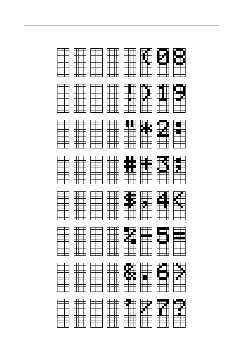
Ў Semiconductor
ML9044
48/54
Relationship Between Character Codes and Character patterns
00H
08H
10H
18H
20H
28H
30H
38H
01H
09H
11H
19H
21H
29H
31H
39H
02H
0AH
12H
1AH
22H
2AH
32H
3AH
03H
0BH
13H
1BH
23H
2BH
33H
3BH
04H
0CH
14H
1CH
24H
2CH
34H
3CH
05H
0DH
15H
1DH
25H
2DH
35H
3DH
06H
0EH
16H
1EH
26H
2EH
36H
3EH
07H
0FH
17H
1FH
27H
2FH
37H
3FH
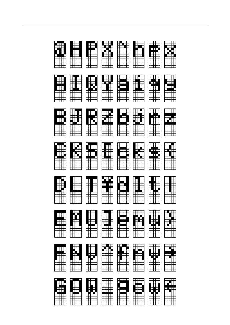
Ў Semiconductor
ML9044
49/54
40H
48H
50H
58H
60H
68H
70H
78H
41H
49H
51H
59H
61H
69H
71H
79H
42H
4AH
52H
5AH
62H
6AH
72H
7AH
43H
4BH
53H
5BH
63H
6BH
73H
7BH
44H
4CH
54H
5CH
64H
6CH
74H
7CH
45H
4DH
55H
5DH
65H
6DH
75H
7DH
46H
4EH
56H
5EH
66H
6EH
76H
7EH
47H
4FH
57H
5FH
67H
6FH
77H
7FH
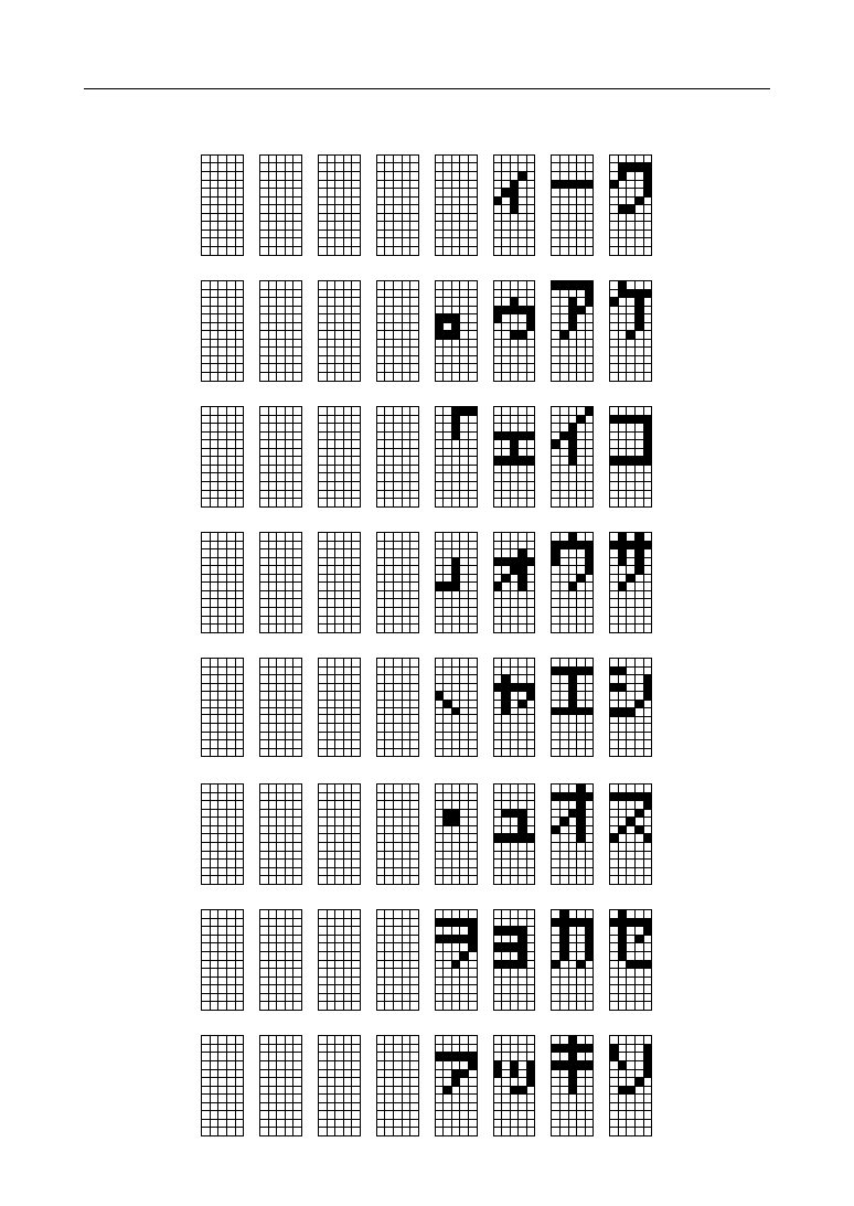
Ў Semiconductor
ML9044
50/54
80H
88H
90H
98H
A0H
A8H
B0H
B8H
81H
89H
91H
99H
A1H
A9H
B1H
B9H
82H
8AH
92H
9AH
A2H
AAH
B2H
BAH
83H
8BH
93H
9BH
A3H
ABH
B3H
BBH
84H
8CH
94H
9CH
A4H
ACH
B4H
BCH
85H
8DH
95H
9DH
A5H
ADH
B5H
BDH
86H
8EH
96H
9EH
A6H
AEH
B6H
BEH
87H
8FH
97H
9FH
A7H
AFH
B7H
BFH

Ў Semiconductor
ML9044
51/54
C0H
C8H
D0H
D8H
E0H
E8H
F0H
F8H
C1H
C9H
D1H
D9H
E1H
E9H
F1H
F9H
C2H
CAH
D2H
DAH
E2H
EAH
F2H
FAH
C3H
CBH
D3H
DBH
E3H
EBH
F3H
FBH
C4H
CCH
D4H
DCH
E4H
ECH
F4H
FCH
C5H
CDH
D5H
DDH
E5H
EDH
F5H
FDH
C6H
CEH
D6H
DEH
E6H
EEH
F6H
FEH
C7H
CFH
D7H
DFH
E7H
EFH
F7H
FFH

Ў Semiconductor
ML9044
52/54
PAD CONFIGURATION
Pad Layout
Chip Size
: 10.62 Ґ 2.55mm
Chip Thickness : 625
±
20mm
Bump Size (1)
: 72 Ґ 72mm
Bump Size (2)
: 54 Ґ 96mm
Pad Coordinates
Y
X
182
183
62
189
56
1
63
55
Pad
Symbol
X (
mm)
Y (
mm)
1099.8
1099.8
1099.8
1099.8
1099.8
1099.8
1099.8
1099.8
1099.8
1099.8
1099.8
1099.8
1099.8
1099.8
1099.8
1099.8
1099.8
1099.8
1099.8
1099.8
1099.8
1099.8
1099.8
1099.8
1099.8
1099.8
1099.8
1099.8
1099.8
1099.8
1099.8
1099.8
1099.8
1099.8
1099.8
1099.8
1099.8
1099.8
1099.8
1099.8
V
1
V
2
V
3A
V
3B
V
4
V
5
V
5IN
V
CC
V
C
V
IN
BEB
V
DD
CSR
SSR
P/S
V
SS
DB
7
DB
6
DB
5
DB
4
5103
4914
4725
4536
4347
4158
3969
3780
3591
3402
3213
3024
2835
2646
2457
2268
2079
1890
1701
1512
Pad
Symbol
X (
mm)
Y (
mm)
DB
3
DB
2
DB
1
DB
0
E
R/W
RS
0
RS
1
SO
SI
SHT
CS
OSC
2
OSC
R
OSC
1
T
3
T
2
T
1
COM
1
COM
2
1323
1134
945
756
567
378
189
0
189
378
567
756
945
1134
1323
1512
1701
1890
2079
2268
1
2
3
4
5
6
7
8
9
10
11
12
13
14
15
16
17
18
19
20
21
22
23
24
25
26
27
28
29
30
31
32
33
34
35
36
37
38
39
40
Ў Semiconductor
ML9044
53/54
Pad
Symbol
X (
mm)
Y (
mm)
COM
3
COM
4
COM
5
COM
6
COM
7
COM
8
COM
9
COM
10
COM
11
COM
12
COM
13
COM
14
COM
15
COM
16
COM
17
DUMMY
DUMMY
DUMMY
DUMMY
DUMMY
2457
2646
2835
3024
3213
3402
3591
3780
3969
4158
4347
4536
4725
4914
5103
5184
5184
5184
5184
5184
Pad
Symbol
X (
mm)
Y (
mm)
SEG
102
SEG
101
SEG
100
SEG
99
SEG
98
SEG
97
SEG
96
SEG
95
SEG
94
SEG
93
SEG
92
SEG
91
SEG
90
SEG
89
SEG
88
SEG
87
SEG
86
SEG
85
SEG
84
3486
3402
3318
3234
3150
3066
2982
2898
2814
2730
2646
2562
2478
2394
2310
2226
2142
2058
1974
1890
41
42
43
44
45
46
47
48
49
50
51
52
53
54
55
56
57
58
59
60
81
82
83
84
85
86
87
88
89
90
91
92
93
94
95
96
97
98
99
100
DUMMY
5184
1806
61
101
DUMMY
5184
1722
62
102
SEG
120
4998
1638
63
103
SEG
119
4914
1554
64
104
SEG
118
4830
1470
65
105
SEG
117
4746
1386
66
106
SEG
116
4662
1302
67
107
SEG
115
4578
1218
68
108
SEG
114
4494
1134
69
109
SEG
113
4410
1050
70
110
SEG
112
4326
966
71
111
SEG
111
4242
882
72
112
SEG
110
4158
798
73
113
SEG
109
4074
714
74
114
SEG
108
3990
630
75
115
SEG
107
3906
546
76
116
SEG
106
3822
462
77
117
SEG
105
3738
378
78
118
SEG
104
3654
294
79
119
SEG
103
3570
SEG
64
SEG
63
210
80
120
1099.8
1099.8
1099.8
1099.8
1099.8
1099.8
1099.8
1099.8
1099.8
1099.8
1099.8
1099.8
1099.8
1099.8
1099.8
720
480
240
0
240
480
720
1087.8
1087.8
1087.8
1087.8
1087.8
1087.8
1087.8
1087.8
1087.8
1087.8
1087.8
1087.8
1087.8
1087.8
1087.8
1087.8
1087.8
1087.8
SEG
83
SEG
82
SEG
81
SEG
80
SEG
79
SEG
78
SEG
77
SEG
76
SEG
75
SEG
74
SEG
73
SEG
72
SEG
71
SEG
70
SEG
69
SEG
68
SEG
67
SEG
66
SEG
65
1087.8
1087.8
1087.8
1087.8
1087.8
1087.8
1087.8
1087.8
1087.8
1087.8
1087.8
1087.8
1087.8
1087.8
1087.8
1087.8
1087.8
1087.8
1087.8
1087.8
1087.8
1087.8
1087.8
1087.8
1087.8
1087.8
1087.8
1087.8
1087.8
1087.8
1087.8
1087.8
1087.8
1087.8
1087.8
1087.8
1087.8
1087.8
1087.8
1087.8
Ў Semiconductor
ML9044
54/54
Pad
Symbol
X (
mm)
Y (
mm)
SEG
62
SEG
61
SEG
60
SEG
59
SEG
58
SEG
57
SEG
56
SEG
55
SEG
54
SEG
53
SEG
52
SEG
51
SEG
50
SEG
49
SEG
48
SEG
47
SEG
46
SEG
45
SEG
44
SEG
43
126
42
42
121
122
123
124
125
126
127
128
129
130
131
132
133
134
135
136
137
138
139
140
SEG
42
141
SEG
41
142
SEG
40
143
SEG
39
144
SEG
38
145
SEG
37
146
SEG
36
147
SEG
35
148
SEG
34
149
1087.8
1087.8
1087.8
1087.8
1087.8
1087.8
1087.8
1087.8
1087.8
1087.8
1087.8
1087.8
1087.8
1087.8
1087.8
1087.8
1087.8
1087.8
1087.8
1087.8
1087.8
1087.8
1087.8
1087.8
1087.8
1087.8
1087.8
1087.8
1087.8
1087.8
1087.8
1087.8
1087.8
1087.8
1087.8
126
210
294
378
462
546
630
714
798
882
966
1050
1134
1218
1302
1386
1470
1554
1638
1722
1806
1890
1974
2058
2142
2226
Pad
Symbol
X (
mm)
Y (
mm)
SEG
27
SEG
26
SEG
25
SEG
24
SEG
23
SEG
22
SEG
21
SEG
20
SEG
19
SEG
18
SEG
17
SEG
16
SEG
15
SEG
14
SEG
13
SEG
12
SEG
11
SEG
10
SEG
9
SEG
8
2814
2898
2982
156
157
158
159
160
161
162
163
164
165
166
167
168
169
170
171
172
173
174
175
SEG
7
176
SEG
6
177
SEG
5
178
SEG
4
179
SEG
3
180
SEG
2
181
SEG
1
182
DUMMY
183
DUMMY
184
1087.8
1087.8
1087.8
1087.8
1087.8
1087.8
1087.8
1087.8
1087.8
1087.8
1087.8
1087.8
1087.8
1087.8
1087.8
1087.8
1087.8
1087.8
1087.8
1087.8
1087.8
1087.8
1087.8
1087.8
1087.8
1087.8
1087.8
720
480
3066
3150
3234
3318
3402
3486
3570
3654
3738
3822
3906
3990
4074
4158
4242
4326
4410
4494
4578
4662
4746
4830
4914
4998
5184
5184
SEG
33
150
2310
DUMMY
185
240
5184
SEG
32
151
2394
DUMMY
186
0
5184
SEG
31
152
2478
DUMMY
187
240
5184
SEG
30
153
2562
DUMMY
188
480
5184
SEG
29
154
2646
DUMMY
189
720
5184
SEG
28
155
2730

NOTICE
1.
The information contained herein can change without notice owing to product and/or
technical improvements. Before using the product, please make sure that the information
being referred to is up-to-date.
2.
The outline of action and examples for application circuits described herein have been
chosen as an explanation for the standard action and performance of the product. When
planning to use the product, please ensure that the external conditions are reflected in the
actual circuit, assembly, and program designs.
3.
When designing your product, please use our product below the specified maximum
ratings and within the specified operating ranges including, but not limited to, operating
voltage, power dissipation, and operating temperature.
4.
Oki assumes no responsibility or liability whatsoever for any failure or unusual or
unexpected operation resulting from misuse, neglect, improper installation, repair, alteration
or accident, improper handling, or unusual physical or electrical stress including, but not
limited to, exposure to parameters beyond the specified maximum ratings or operation
outside the specified operating range.
5.
Neither indemnity against nor license of a third party's industrial and intellectual property
right, etc. is granted by us in connection with the use of the product and/or the information
and drawings contained herein. No responsibility is assumed by us for any infringement
of a third party's right which may result from the use thereof.
6.
The products listed in this document are intended for use in general electronics equipment
for commercial applications (e.g., office automation, communication equipment,
measurement equipment, consumer electronics, etc.). These products are not authorized
for use in any system or application that requires special or enhanced quality and reliability
characteristics nor in any system or application where the failure of such system or
application may result in the loss or damage of property, or death or injury to humans.
Such applications include, but are not limited to, traffic and automotive equipment, safety
devices, aerospace equipment, nuclear power control, medical equipment, and life-support
systems.
7.
Certain products in this document may need government approval before they can be
exported to particular countries. The purchaser assumes the responsibility of determining
the legality of export of these products and will take appropriate and necessary steps at their
own expense for these.
8.
No part of the contents contained herein may be reprinted or reproduced without our prior
permission.
9.
MS-DOS is a registered trademark of Microsoft Corporation.
Copyright 1999 Oki Electric Industry Co., Ltd.
Printed in Japan
E2Y0002-29-62