
OKI Semiconductor
PEDL9055A-02-01
Issue Date: Jul. 26, 2002
ML9055A-02
Preliminary
LCD Controller/Driver
1/59
GENERAL DESCRIPTION
The ML9055A-02 is an LSI providing the bit map display on a dot matrix graphic LCD panel . With one chip, it is
possible to construct a graphic display system with a maximum of 128
�
128 dots. Since all the functions necessary
for driving the bit map type LCD panel are incorporated into a single chip, the ML9055A-02 allows to implement a
dot matrix graphic LCD display system of bit map type with only a few chips in combination with an 8-bit
microcomputer.
Using the CMOS process and a built-in RAM, the ML9055A-02 is highly suitable for displays in battery-operated
portable equipment.
FEATURES
� Liquid Crystal Display (LCD) controller and driver
� Maximum display size: 128 columns
�
128 rows
� Logic voltage: 1.8 to 3.0 V
� LCD drive voltage: 4.0 to 16.0 V
� Serial interface (3-line or 4-line, write only) and parallel interface
� Built-in voltage multiplier and oscillator circuit for display timing control
� LCD drive bias: 1/5 to 1/12
� Duty ratio: 1/16 to 1/128
� Voltage regulator temperature coefficient: �0.125%/
o
C
� Voltage multiplier: x3, x4, x5, x6
� Contrast adjustjment: 64 levels available
� 4-level gray scale
� Partial display function
� Scroll
function
� Frame frequency: 180 Hz
� Package: Gold bump chip, TCP
ML9055A-02DVWA (Gold bump chip name)
ML9055A-02DVVAZ01L (General TCP name)

PEDL9055A-02-01
1Semiconductor
ML9055A-02
2/59
BLOCK DIAGRAM
128-Segment
Driver Circuit
128-Common
Driver Circuit
Segment Controller
Common Controller
COM127
COM0
COM1
COM2
COM125
COM126
SEG127
SEG
0
SEG
1
SEG
2
SEG125
SEG126
V0
V4
V3
V2
V1
V
DD
V
SS
Oscillation Circuit
/
Display
Timing
Control
TEST1
Voltage
Follower
Circuit
Voltage
Multiplier
Circuit
Voltage
Regulator
Circuit
VOUT
INTRS
REF
VEXT
VR
C5+
C4+
C3+
C2�
C2+
C1�
C1+
VCI
Display Data
RAM
Line
Address
Circuit
Column
Address
Circuit
Instruction
Register
Microcomputer Interface Logic
DB0
DB7
(
SDATA
)
DB6
(
SCLK
)
DB5 DB4 DB3 DB2 DB1
E
(
RD
)
R/W
(
WR
)
RESET
PS0 PS1
CS
RS
Status
Register
...
...
TEST2
Page
Address
Circuit
I/O
Buffer

PEDL9055A-02-01
1Semiconductor
ML9055A-02
3/59
PIN CONFIGURATION (STANDARD TCP: BRONZE-FOIL FACE UP)
NC1
PS0
PS1
CS
RESET
RS
R/W (WR)
E (RD)
DB0
DB1
DB2
DB3
DB4
DB5
DB6
DB7
V
DD
VCI
V
SS
VOUT
C5+
C3+
C1�
C1+
C2+
C2�
C4+
REF
VEXT
INTRS
V4
V3
V2
V1
V0
VR
TEST1
NC2
NC
NC1
COM113
COM112
COM111
COM110
COM66
COM65
COM64
SEG127
SEG126
SEG2
SEG1
SEG0
COM14
COM15
COM60
COM61
COM62
COM63
NC
NC2
Note 1: This drawing is not a true external view of TCP, but it primarily shows the TCP pin layout.
Note 2: The TCP shown above is a standard TCP and does not have COM0 to COM13 pins and
COM114 to COM127 pins. Also there is no TEST2 pin on the TCP.
(In the TCP, 128 lines from SEG0 to SEG127 and 100 lines from COM14 to COM113 are
derived as the output pins.)
The external shape and the number of output pins of TCP can be customized as needed.
Note 3: Do not connect the NC pins to outside or any other pins. NC stands for "No Connection". The NC
pins are not connected to the chip. All NC pins are independent.
NC1 remains connected to COM112 before dicing. Although the input side NC1 remains
connected with the output side NC1 by dicing, the connection with COM112 is lost.
Similarly, NC2 remains connected to COM63 before dicing. Although the input side NC2
remains connected with the output side NC2 by dicing, the connection with COM63 is lost.

PEDL9055A-02-01
OKI Semiconductor
ML9055A-02
4/59
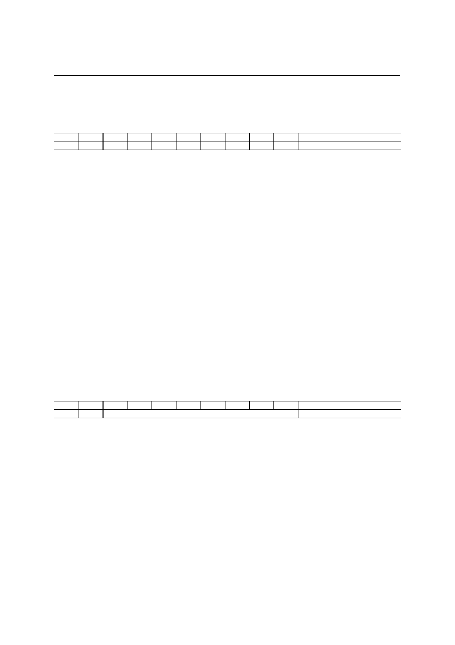
PIN DESCRIPTIONS
Function Symbol
Type
Description
V
DD
Supply
Power
supply
V
SS
Supply
Ground
V0
V1
V2
V3
Power Supply
V4
I/O
LCD drive power supply voltage pin V0, and LCD drive bias
voltage pins V1 to V4
When applying the LCD drive power supply voltage and each
LCD drive bias voltage from outside, notice to hold the following
relationship:
V
SS
< V4 < V3 < V2 < V1 < V0
The LCD drive bias voltages are generated when using the
built-in voltage follower.
For the value of each generated bias voltage, refer to the
"Voltage Follower Circuit" section in this document.
C1� O
C1+ O
C2� O
C2+ O
C3+ O
C4+ O
C5+ O
Connection pins of capacitors for multiplied voltage
Connect capacitors for the voltage multiplier to these pins.
(Connect pins with + sign to positive polarity of respective
capacitors and pins with � sign to negative polarity of respective
capacitors.)
The connections of capacitors for multiplying voltage differ
depending upon the voltage multiplication.
The connections of the capacitors for multiplying voltage are
described in the "Voltage Multiplier" section.
VOUT I/O
Voltage multiplier input/output pins
When using an internal voltage multiplier, the following voltage is
output from the VOUT pin:
VOUT = VCI x Voltage multiplication
When not using the internal voltage multiplier, input the external
power supply voltage from this VOUT pin.
About the pin processing in the case of an external input, refer to
the "LCD Drive Power Supply Circuit" section.
VCI I
Multiplied voltage input pin of internal voltage multiplier
When using an external power supply, tie this pin to V
SS
.
VR I
V0 voltage adjustment pin (Adjusts V0 using external resistors.)
When INTRS pin = "L", the V0 voltage is adjusted by connecting
external resistors to this pin.
The method of connecting external resistors is described in the
"LCD Drive Power Supply Circuit" section.
When INTRS pin = "H", keep this VR pin open.
Note: When INTRS pin is "H", the internal resistors are selected
for adjusting V0 and a very high internal resistor gets connected
to VR pin. Therefore this ML9055A can be vulnerable to external
noise. In designing the circuit board, pay proper attention to the
external noise and leak.
REF I
Internal/external reference voltage select pin. (L: External, H:
Internal)
VEXT I
External reference voltage (V
REF
) input pin. (Valid only when
REF= L.)
When using the internal reference power supply, keep this pin
open.
LCD Driver Supply
INTRS I
V0 adjustment resistor select pin (L: External, H: Internal)

PEDL9055A-02-01
OKI Semiconductor
ML9055A-02
5/59
Function Symbol
Type
Description
RESET
I
Reset input pin (active "L")
PS0
PS1
I
Parallel/serial data setting (H = Parallel, L = Serial)
Note: When using the serial interface, leave D0-D5 open and
connect E (RD) and R/W (WR) to V
DD
or V
SS
.
CS
I
Chip select input pin (active "L")
RS I
Register select input pin
Distinguishes between display data (H) and command data (L).
Connect this pin to V
DD
or V
SS
for 3-line serial interface.
R/W (WR)
I
When connected to a 68-series MPU: Read/write execute
control pin
(H = read, L = write)
When connected to an 80-series MPU: Write execute control pin
(L = write)
E (RD)
I
When connected to a 68-series MPU: E clock input pin
When connected to an 80-series MPU: Read execute control pin
(L = read)
Microcomputer
Interface
DB0 to
DB7
I/O
When parallel interface is selected,
8-bit data bus pin
When serial interface is selected,
DB0 to DB5: Open
DB6(SCLK): Serial clock input
DB7(SDATA): Serial data input
SEG0 to
SEG127
O
LCD segment driver outputs
LCD Driver
COM0 to
COM127
O
LCD common driver outputs
TEST1
I
Test pin of this LSI. Connect this pin to V
DD.
Test
TEST2
O
Test pin of this LSI. Leave this pin open
PS0 PS1
Interface
L
L
3-line serial interface
L
H
4-line serial interface
H
L
8080 parallel interface
H
H
6800 parallel interface

PEDL9055A-02-01
OKI Semiconductor
ML9055A-02
6/59
ABSOLUTE MAXIMUM RATINGS
(V
SS
= 0 V)
Parameter Symbol
Condition
Rating Unit
Power Supply Voltage
V
DD
Tj = 25�C
�0.3 to +4.0
V
Voltage Multiplier Input
Voltage
VCI
Tj = 25�C
�0.3 to +4.0 (*1)
V
Voltage Multiplier Output
Voltage
VOUT
Tj = 25�C
�0.3 to +20.0
V
LCD Drive Voltage
V0
Tj = 25�C
�0.3 to +20.0 (*2)
V
LCD Drive Bias Voltage
Vm (*3)
Tj = 25�C
�0.3 to V0 +0.3 (*4)
V
Logic Input Voltage
V
I
Tj = 25�C
�0.3 to V
DD
+0.3
V
Storage Temperature
Range
T
stg
Chip
�55 to +150
�C
*1. Notice that voltage multiplier output voltage VOUT should not exceed 20 V.
*2. V0 should not exceed VOUT.
*3. Vm indicates V1, V2, V3 and V4.
*4. Notice that Vm should not exceed 20 V.
RECOMMENDED OPERATING CONDITIONS
(V
SS
= 0 V)
Parameter Symbol
Condition
Range Unit
Power Supply Voltage
V
DD
--
1.8 to 3.0
V
Voltage Multiplier Input
Voltage
VCI --
V
DD
to 3.0 (*1)
V
Voltage Multiplier Output
Voltage
VOUT
--
5.4 to 16.0
V
LCD Driver voltage
V0
--
4.0 to VOUT�1
V
LCD Driver Bias Voltage 1
V1
--
3.2 to 14.7 (*2)
V
LCD Driver Bias Voltage 2
V2
--
2.4 to 13.4 (*2)
V
LCD Driver Bias Voltage 3
V3
--
1.6 to 2.7 (*2)
V
LCD Driver Bias Voltage 4
V4
--
0.8 to 1.4 (*2)
V
External Reference
Voltage
VEXT
--
1.8 to V
DD
V
Operating Temperature
T
jop
Chip
�40 to +85
�C
*1. Notice that the voltage multiplier output voltage VOUT is 16 V or below.
*2. Notice that VOUT>V0>V1>V2>V3>V4.
Do not expose the ML9055A to light when in use.

PEDL9055A-02-01
OKI Semiconductor
ML9055A-02
7/59
ELECTRICAL CHARACTERISTICS
DC Characteristics
(V
DD
= 1.8 to 3.0 V, V
SS
= 0 V, Tj = �40 to +85�C)
Parameter Symbol Condition
Min.
Typ.
Max.
Unit
Applied
pins
High Input Voltage
V
IH
--
0.8
�
V
DD
-- V
DD
V
Low Input Voltage
V
IL
-- 0.0
--
0.2
�
V
DD
V
RESET, PS0,
PS1, CS, RS,
R/W (WR),
E (RD),
DB7 (SDATA),
DB6 (SCLK),
DB5�DB0,
INTRS,
REF
High Output Voltage
V
OH
I
OH
= �0.5 mA
0.8
�
V
DD
-- V
DD
V
Low Output Voltage
V
OL
I
OL
= 0.5 mA
0.0
--
0.2
�
V
DD
V
DB7 (SDATA),
DB6 (SCLK),
DB5�DB0
Input Current
I
IL
V
IN
= V
DD
or V
SS
�1.0
+1.0
�
A
RESET, PS0,
PS1, CS, RS,
R/W (WR),
E (RD),
DB7 (SDATA),
DB6 (SCLK),
DB5�DB0,
INTRS,
REF
LCD Driver On
Resistance
R
ON
Tj = 25�C,
1/8 bias
V0 = 8 V
-- 2.5 5 k
SEG0�SEG127,
COM0�COM127
Internal resistance
ratio error
R
ratio
-- --
--
3
%
V0
VOUT-V0 Voltage
V
OT0
V0 load current = 300
�
A
VOUT = 8 V(applied
externally)
LCD output, no load
1 -- --
V VOUT,
V0

PEDL9055A-02-01
OKI Semiconductor
ML9055A-02
8/59
Parameter Symbol
Condition
Min.
Typ.
Max.
Unit
Applied pins
I
DD11
Tj= 25
o
C,
V
DD
= VCI = 2.75 V
�
5 voltage multiplier
1/100 duty
Frame frequency: 180 Hz
Display: Off (*1)
-- 150 230
�
A
I
DD12
Tj= 25
o
C,
V
DD
= VCI = 2.75 V
�
5 voltage multiplier
1/128 duty
Frame frequency: 220 Hz
Display: Off (*1)
-- 185 285
�
A
I
DD21
Tj= 25
o
C,
V
DD
= VCI = 2.75 V
�
5 voltage multiplier
Display: On
1/100 duty
Frame frequency: 180 Hz
(Full checker board
pattern (*1)
-- 300 430
�
A
Operating Current
Consumption
I
DD22
Tj= 25
o
C,
V
DD
= VCI = 2.75 V
�
5 voltage multiplier
Display: On
1/128 duty
Frame frequency: 220 Hz
(Full checker board
pattern (*1)
-- 370 530
�
A
Current Consumption
in Power Save Mode
I
SLEEP
Power save mode
Tj = 25�C, V
DD
= 3.0 V
-- -- 2
�
A
V
DD
, VCI (*2)
Voltage Multiplier
Efficiency
E
VC
�
3/
�
4/
�
5/
�
6
Using internal power
supply
No load
95 99 -- %
VOUT
Tj = �20�C
--
2.22
--
V
Tj = 25�C
2.04
2.10
2.16
V
Reference Voltage
V
REF
Tj = 70�C
--
1.98
--
V
VEXT (*3)
(*1) No CPU access state.
No LCD panel load.
Other conditions: 1/12 bias; contrast = 60; internal resistance ratio setting = 5.8; 3-FRC; 9-level
PWM; frame inversion
(*2) The current consumption is a sum of V
DD
current and VCI current.
(*3) Vref voltage is measurable in the test mode, but cannot be measured when a customer is using the
ML9055A in normal circumstances.

PEDL9055A-02-01
OKI Semiconductor
ML9055A-02
9/59
AC Characteristics
Serial Interface Timing
(V
DD
= 1.8 V, Tj = �40 to +85�C)
Parameter Symbol
Min.
Typ.
Max.
Unit
Serial Clock Frequency
f
CLK
--
-- 9
MHz
Serial Clock Cycle Time
t
CLK
111 -- -- ns
Serial Clock "H" Pulse Width
t
WHS
50 -- -- ns
Serial Clock "L" Pulse Width
t
WLS
50 -- -- ns
Data Setup Time
t
DS
50 -- -- ns
Data Hold Time
t
DH
50 -- -- ns
Chip Select Setup Time
t
CSS
60 -- -- ns
Chip Select Hold Time
t
CSH
50 -- -- ns
Chip Select "H" Pulse Width
t
CH
50 -- -- ns
Register Select Setup Time(*1)
t
RSS
60 -- -- ns
Register Select Hold Time(*1)
t
RSH
60 -- -- ns
Input Signal Rise Time (*2)
tr
--
-- 15 ns
Input Signal Fall Time (*2)
tf
--
-- 15 ns
(Note) (*1) Not applied to 3-line serial interface.
(*2) Applied to all input pins.
(V
DD
= 2.7 V, Tj = �40 to +85�C)
Parameter Symbol
Min.
Typ.
Max.
Unit
Serial Clock Frequency
f
CLK
--
-- 17
MHz
Serial Clock Cycle Time
t
CLK
58.8 -- -- ns
Serial Clock "H" Pulse Width
t
WHS
25 -- -- ns
Serial Clock "L" Pulse Width
t
WLS
25 -- -- ns
Data Setup Time
t
DS
25 -- -- ns
Data Hold Time
t
DH
25 -- -- ns
Chip Select Setup Time
t
CSS
30 -- -- ns
Chip Select Hold Time
t
CSH
25 -- -- ns
Chip Select "H" Pulse Width
t
CH
30 -- -- ns
Register Select Setup Time(*1)
t
RSS
30 -- -- ns
Register Select Hold Time(*1)
t
RSH
30 -- -- ns
Input Signal Rise Time (*2)
tr
--
-- 15 ns
Input Signal Fall Time (*2)
tf
--
-- 15 ns
(Note) (*1) Not applied to 3-line serial interface.
(*2) Applied to all input pins.

PEDL9055A-02-01
OKI Semiconductor
ML9055A-02
10/59
Parallel Interface Timing (68-series MPU)
(V
DD
= 1.8 V, Tj = �40 to +85�C)
Parameter Symbol
Condition
Min.
Typ.
Max.
Unit
Address Setup Time
t
AS
-- 0 -- --
ns
Address Hold Time
t
AH
-- 0 -- --
ns
CS "L" Pulse Width for Write
t
CSL
-- 60 -- --
ns
CS "H" Pulse Width for Write
t
CSH
-- 60 -- -- ns
CS "L" Pulse Width for Read
t
CSL
-- 100 -- --
ns
CS "H" Pulse Width for Read
t
CSH
-- 100 -- -- ns
E "H" Pulse Width for Write
t
EH
-- 60 -- --
ns
E "L" Pulse Width for Write
t
EL
-- 60 -- --
ns
E "H" Pulse Width for Read
t
EH
-- 100
-- --
ns
E "L" Pulse Width for Read
t
EL
-- 100
-- --
ns
Data Setup Time
t
DS
-- 40 -- --
ns
Data Hold Time during Write
t
DH
-- 10 -- --
ns
Data Access Time
t
ACC
C
L
= 100 pF
--
--
90
ns
Data Hold Time during Read
t
OH
-- 10 -- 90
ns
System Write Cycle Time
t
CYC
-- 150 -- -- ns
System Read Cycle Time
t
CYC
-- 330 -- -- ns
Input Signal Rise Time (*1)
tr
--
--
--
15
ns
Input Signal Fall Time (*1)
tf
--
--
--
15
ns
(Note) (*1) Applied to all input pins.
(V
DD
= 2.7 V, Tj = �40 to +85�C)
Parameter Symbol
Condition
Min.
Typ.
Max.
Unit
Address Setup Time
t
AS
-- 0 -- --
ns
Address Hold Time
t
AH
-- 0 -- --
ns
CS "L" Pulse Width for Write
t
CSL
-- 40 -- --
ns
CS "H" Pulse Width for Write
t
CSH
-- 40 -- -- ns
CS "L" Pulse Width for Read
t
CSL
-- 60 -- --
ns
CS "H" Pulse Width for Read
t
CSH
-- 60 -- -- ns
E "H" Pulse Width for Write
t
EH
-- 40 -- --
ns
E "L" Pulse Width for Write
t
EL
-- 40 -- --
ns
E "H" Pulse Width for Read
t
EH
-- 60 -- --
ns
E "L" Pulse Width for Read
t
EL
-- 60 -- --
ns
Data Setup Time
t
DS
-- 30 -- --
ns
Data Hold Time during Write
t
DH
-- 5 -- --
ns
Data Access Time
t
ACC
C
L
= 100 pF
--
--
50
ns
Data Hold Time during Read
t
OH
-- 10 -- 50
ns
System Write Cycle Time
t
CYC
-- 150 -- -- ns
System Read Cycle Time
t
CYC
-- 166 -- -- ns
Input Signal Rise Time (*1)
tr
--
--
--
15
ns
Input Signal Fall Time (*1)
tf
--
--
--
15
ns
(Note) (*1) Applied to all input pins.

PEDL9055A-02-01
OKI Semiconductor
ML9055A-02
11/59
Parallel Interface Timing (80-series MPU)
(V
DD
= 1.8 V, Tj = �40 to +85�C)
Parameter Symbol
Condition
Min.
Typ.
Max.
Unit
Address Setup Time
t
AS
-- 0 -- --
ns
Address Hold Time
t
AH
-- 0 -- --
ns
CS, WR "L" Pulse Width for Write
t
CSL
-- 60 -- --
ns
CS, WR "H" Pulse Width for Write
t
CSH
-- 60 -- --
ns
CS, RD "L" Pulse Width for Read
t
CSL
-- 100 -- --
ns
CS, RD "H" Pulse Width for Read
t
CSH
-- 100 -- --
ns
Data Setup Time
t
DS
-- 40 -- --
ns
Data Hold Time during Write
t
DH
-- 10 -- --
ns
Data Access Time
t
ACC
C
L
= 100 pF
--
--
90
ns
Data Hold Time during Read
t
OH
-- 10 -- 90
ns
System Write Cycle Time
t
CYC
-- 150 -- --
ns
System Read Cycle Time
t
CYC
-- 330 -- --
ns
Input Signal Rise Time (*1)
tr
--
--
--
15
ns
Input Signal Fall Time (*1)
tf
--
--
--
15
ns
(Note) (*1) Applied to all input pins.
(V
DD
= 2.7 V, Tj = �40 to +85�C)
Parameter Symbol
Condition
Min.
Typ.
Max.
Unit
Address Setup Time
t
AS
-- 0 -- --
ns
Address Hold Time
t
AH
-- 0 -- --
ns
CS, WR "L" Pulse Width for Write
t
CSL
-- 40 -- --
ns
CS, WR "H" Pulse Width for Write
t
CSH
-- 40 -- --
ns
CS, RD "L" Pulse Width for Read
t
CSL
-- 60 -- --
ns
CS, RD "H" Pulse Width for Read
t
CSH
-- 60 -- --
ns
Data Setup Time
t
DS
-- 30 -- --
ns
Data Hold Time during Write
t
DH
-- 5 -- --
ns
Data Access Time
t
ACC
C
L
= 100 pF
--
--
50
ns
Data Hold Time during Read
t
OH
-- 10 -- 50
ns
System Write Cycle Time
t
CYC
-- 150 -- --
ns
System Read Cycle Time
t
CYC
-- 166 -- --
ns
Input Signal Rise Time (*1)
tr
--
--
--
15
ns
Input Signal Fall Time (*1)
tf
--
--
--
15
ns
(Note) (*1) Applied to all input pins.

PEDL9055A-02-01
OKI Semiconductor
ML9055A-02
12/59
OSC Frequency
(V
DD
= 1.8 to 3.0 V, Tj = 25�C)
Parameter Symbol Condition Min.
Typ.
Max.
Unit
9PWM, 1/100 duty
150
180
210
Hz
Frame Frequency
f
FR
9PWM, 1/128 duty
180
220
260
Hz
Reset Timing
(V
DD
= 1.8 to 3.0 V, Tj = �40 to +85�C)
Parameter Symbol Condition Min.
Typ.
Max.
Unit
Reset Pulse Width
t
RES
--
1.5
--
--
�
s
Input Signal Rise Time
tr
--
--
--
15
ns
Input Signal Fall Time
tf
--
--
--
15
ns

PEDL9055A-02-01
OKI Semiconductor
ML9055A-02
13/59
TIMING DIAGRAMS
3- and 4-Line Serial Interface Timing Diagram
V
IH
= 0.8V
DD
V
IL
= 0.2V
DD
In 3-line system, the ML9055A interfaces with a microcomputer by 3 lines namely,
CS, SCLK, and
SDATA.
The method to switch between the data and command in the 3-line system is described in the
"Microcomputer Interface" section of Functional Description.
In 4-line system, the ML9055A interfaces with a microcomputer by 4 lines namely
CS, SCLK, SDATA,
and RS.
If
CS holds "L", the display data and command write operations can be executed consecutively. At this time,
the chip select setup time, t
CSS
, stipulates the time up to the first falling edge of SCLK after the falling edge
of
CS. And the chip select hold time, t
CSH,
stipulates the time from the rising edge of the last SCLK up to the
rising edge of
CS.
DB0
V
IL
DB6
0.9V
DD
0.1V
DD
0.9V
DD
CS
SCLK
SDATA
RS
t
CSS
t
CSH
t
CLK
t
DS
V
IL
V
IL
V
IH
V
IL
0.1V
DD
0.1V
DD
0.9V
DD
0.1V
DD
t
DH
V
IH
V
IH
V
IL
DB7
DB1
t
WLS
t
WHS
t
RSS
t
RSH
V
IH
V
IL
0.1V
DD
t
r
t
f
0.9V
DD
t
CH
DB7
V
IH

PEDL9055A-02-01
OKI Semiconductor
ML9055A-02
14/59
Parallel Interface Timing Diagram for 68-Series MPU
V
IH
= 0.8V
DD
V
IL
= 0.2V
DD
V
OH
= 0.8V
DD
V
OL
= 0.2V
DD
Note 1: The trace impedance (specially, the V
DD
, V
SS
, VCI impedance and the data bus trace
capacitance etc,) between this chip and circuit board should be designed as low as possible.
Factors such as not sufficiently low trace impedance, LCD panel of large size, and high trace
impedance of the microcomputer interface, would become a cause of the ML9055A malfunction.
In such a situation, use the microcomputer interface not for reading, but for writing only to
reduce the power supply noise.
Note 2: The system cycle time t
CYC
at write and at read is different in the ML9055A. Please keep to the
system write time cycle when switching from the write operation to the read operation and,
similarly, keep to the system read time cycle when switching from the read operation to the write
operation.
Note 3: The overlapping duration when CS is "L" and E is "H" must satisfy t
CSL
or t
EH
. Reference points
t
AS
and t
ACC
in this case are decided by CS or E, whichever is slower, and the reference points t
AH
,
t
DS
, T
DH
and t
OH
are decided by CS or E, whichever is faster.
V
IH
t
CSH
RS, R/W
CS
E
DB7-DB0
(Write)
DB7-DB0
(Read)
t
AS
t
AH
t
CSL
t
CYC
t
EH
t
EL
t
DS
t
DH
t
ACC
t
OH
V
IH
V
IL
V
IH
V
IL
V
IH
V
IL
V
IL
V
OH
V
OL
V
OH
V
OL
0.1V
DD
0.9V
DD
0.1V
DD
0.9V
DD
0.9V
DD
0.9V
DD
0.1V
DD
0.1V
DD
0.1V
DD
t
r
t
f
0.9V
DD

PEDL9055A-02-01
OKI Semiconductor
ML9055A-02
15/59
Parallel Interface Timing Diagram for 80-Series MPU
V
IH
= 0.8V
DD
V
IL
= 0.2V
DD
V
OH
= 0.8V
DD
V
OL
= 0.2V
DD
Note 1: The trace impedance (specially, the V
DD
, V
SS
, VCI impedance and the data bus trace
capacitance etc.,) between this chip and circuit board should be designed as low as possible.
Factors such as not sufficiently low trace impedance, LCD panel of large size, and high trace
impedance of the microcomputer interface, would become a cause of the ML9055A malfunction.
In such a situation, use the microcomputer interface not for reading, but for writing only to
reduce the power supply noise.
Note 2: The system cycle time t
CYC
at write and at read is different in the ML9055A. Please keep to the
system write time cycle when switching from the write operation to the read operation and,
similarly, keep to the system read time cycle when switching from the read operation to the write
operation.
Reset Timing
V
IH
0.9V
DD
t
CSH
V
IH
RS
CS, RD
WR
DB7-DB0
(Write)
DB7-DB0
(READ)
t
AS
t
AH
t
CSL
t
CYC
t
DS
t
DH
t
ACC
t
OH
V
IH
V
IL
V
IL
V
IH
V
IL
V
IL
V
OH
V
OL
V
OH
V
OL
0.1V
DD
0.9V
DD
0.1V
DD
0.9V
DD
t
r
t
f
RESET
t
RES
0.1 V
DD
0.1 V
DD
0.9 V
DD
0.9 V
DD
t
r
t
f

PEDL9055A-02-01
OKI Semiconductor
ML9055A-02
16/59
FUNCTIONAL DESCRIPTION
Microcomputer Interface
� Serial
Interface
The ML9055A communicates with a microcomputer via clock-synchronized serial interface when PS0 holds "L".
Read operation is inhibited in the serial interface. Write operation is executed only when
CS is low.
Data should be input from the most signification bit (MSB). The data latches to the internal shift registers on the
rising edge of the serial clock SCLK, and then processed as 8-bit data on the rising edge of the 8th clock. When
display data is written to the RAM, the column address is incremented automatically by one only. If
CS holds "L",
the serial data can be input continuously. If
CS goes "H" before 8 serial clocks are sent while the serial data is
being input, the discontinued bytes become an invalid data, but the data transmitted prior to that is valid.
The serial interface includes a 3-line serial interface and a 4-line serial interface.
When PS1 is "L", the 3-line serial interface is selected. The 3-line serial interface is composed of serial data
(SDATA), serial clock (SCLK), and chip select (
CS). The set display data length command identifies whether the
data from a microcomputer is a display data or a command data. The specified number of bytes (1 to 256) in data
that follow the set display data length command is processed as the display data. And the next byte, after sending
the number of display data bytes specified by the set display data length command, is processed as the command
data.
If
CS goes "H" while the number of bytes of serial data specified by the set display data length command is being
input, the discontinued bytes become an invalid data. And the bytes sent prior to the transmitted data is a valid data.
The next input data will be processed as the command data.
When PS1 is "H", the 4-line serial interface is selected. The 4-line serial interface is composed of serial data
(SDATA), serial clock (SCLK), chip select (
CS), and register select (RS). The register select pin RS is used to
differentiate whether the data sent from a microcomputer is a display data or a command data. At RS pin = "H", the
input data is a display data. And at RS pin = "L", the input data is a command data.
Note: Do not use the ML9055A with
CS tied to "L". Make sure to return the CS to "H" at the end of a command
or data input. However, use the ML9055A with
CS at "L" when the set display data length command only is
input, including the input data, at the end of this command. Return the
CS to "H" at the end of all data input.

PEDL9055A-02-01
OKI Semiconductor
ML9055A-02
17/59
� Parallel
Interface
The ML9055A communicates with a microcomputer via the parallel interface when the PS0 is "H". The
ML9055A includes a parallel interface for 68-series MPU and a parallel interface for 80-series MPU.
When both PS0 and PS1 are "H", the interface is an 8-bit parallel interface for 68-series MPU. Both read and write
operations are performed only when the Chip Select (
CS) pin is "L"and E clock (E) pin is "H". The Register Select
(RS) pin is used to discriminate whether the data accessed from a microcomputer is a display data or a command
data. When the RS pin is "H", the accessed data is a display data. And when the RS pin is "L", the accessed data is
a command data.
Table 1-1. Parallel Interface Function (68-series MPU)
(
�
Don't care)
E clock (E)
Register
Select (RS)
Chip Select
(CS)
Read/Write
(R/W)
Operation
H
L
L
L
Write command data.
H L L H
Read
status
register.
H
H
L
L
Write display data.
H
H
L
H
Read display data.
L
�
�
�
Invalid
�
�
H
�
Invalid
When PS0 is "H" and PS1 is "L", the interface is an 8-bit parallel interface for 80-series MPU. Both read and write
operations are performed only when the Chip Select (
CS) is "L". The Register Select (RS) pin is used to
discriminate whether the data accessed from a microcomputer is a display data or a command data. When the RS
pin is "H", the accessed data is a display data. And when the RS pin is "L", the accessed data is a command data.
Table 1-2. Parallel Interface Function (80-series MPU)
(
�
Don't care)
Chip Select
(CS)
Register
Select (RS)
Write (WR) Read
(RD)
Operation
L
L
L
H
Write command data.
L
L
H
L
Read status register.
L H L H
Write
display
data.
L H H L
Write
display
data.
L
�
H H
Invalid
H
�
�
�
Invalid
Note: Do not simultaneously input "L" to WR and RD to avoid the ML9055A malfunction.

PEDL9055A-02-01
OKI Semiconductor
ML9055A-02
18/59
LCD Drive Power Supply Circuit
The LCD drive power supply circuit composed of a voltage multiplier (VC), a voltage regulator (VR), and a
voltage follower (VF) is controlled by the set power supply configuration instruction.
Table 2. Power Supply Circuit Configuration
LCD drive power supply circuit
Pin state
(Note 2)
Configuration
Power supply
configuration
(Note 1)
(VC VR VF)
VC
VR
VF
VOUT
V0
V1 � V4
All internal LCD drive
power supply circuits
used
1 1 1
ON
ON
ON
Output
Output
Output
Voltage regulator and
voltage follower used
0 1 1
OFF
ON
ON
External
input
Output Output
Voltage follower only
used
0 0 1
OFF
OFF
ON
Shorted
with V0
External
input
Output
External power supply
used
0 0 0
OFF
OFF
OFF
Shorted
with V0
External
input
External
input
Note 1: Although the set power supply configuration instruction allows to input commands to perform
settings also of combinations other than shown in Table 2, do not perform such settings as
would cause the ML9055A malfunction.
Note 2: When the pin state is "output", connect the specified capacitors to VOUT, V0 and V1 to V4.
� Voltage
multiplier
The voltage multiplier is used to increase the VCI voltage applied to VCI pin up to the set multiple value. The
setting enable voltage multiples are
�
3,
�
4,
�
5, and
�
6. These multiples are set by the voltage multiplication
instruction. After voltage multiplication, the voltage is output from VOUT pin, which is used as a power supply for
the voltage regulator and voltage follower.
A voltage multiplier is configured in conjunction with external capacitors. As shown in Figure 1, to configure
�
3 to
�
6 multiplications, connect appropriate capacitors to the chip externally. Connect the capacitors to configure a
voltage multiplier with the maximum multiplication used. Do not set the voltage multiplication by a command
larger than the enable setting by the external capacitors because it would become a cause of the ML9055 unstable
operation.
Note: Use the voltage multiplier output voltage VOUT, and the LCD drive voltage V0, at the recommended
operating voltage 16.0 V or below.
Figure 1. Voltage Multiplier Setting (C = 0.8
�
F to 5.7
�
F)
Vss
VOUT
C5+
C3+
C1�
C1+
C2+
C2�
C4+
Vss
VOUT
C5+
C3+
C1�
C1+
C2+
C2�
C4+
x3 voltage
multiplication
x4 voltage
multiplication
+
�
+
�
+
�
+
�
+
�
+
�
+
�
Vss
VOUT
C5+
C3+
C1�
C1+
C2+
C2�
C4+
x5 voltage
multiplication
+
�
+
�
+
�
+
�
+
�
Vss
VOUT
C5+
C3+
C1�
C1+
C2+
C2�
C4+
x6 voltage
multiplication
+
�
+
�
+
�
+
�
+
�
+
�

PEDL9055A-02-01
OKI Semiconductor
ML9055A-02
19/59
� Voltage Regulator Circuit
Figure 2. Voltage Regulator Circuit
The voltage regulator is composed of an internal reference voltage circuit, an electronic volume circuit, and an
amplifier circuit. The internal reference voltage circuit outputs the reference voltage, V
REF
= 2.1 V (Tj = 25
o
C).
This reference voltage V
REF
has a temperature co-efficient of 0.125%/
o
C.
The reference voltage V
REF
is input to the electronic volume circuit. V
REF
can be input from VEXT pin also by the
set REF pin instruction. (Refer to Table 3.)
Table 3. V
REF
Voltage at Tj = 25�C
REF Temp.
coefficient
V
REF
(V)
L
(Depends on externally
connected power supply.)
VEXT pin value
H
�0.125%/
�
C
2.1 V
The electronic volume circuit converts the input reference voltage, V
REF,
to the contrast control voltage, Vcon,
expressed by the following equation:
V
CON
= (1
-
(63
-
a)/210)
�
V
REF
Here, parameter "a" is the contrast setting value shown in Table 4. (Levels 0 to 63 can be set.)
+
�
V
CON
VOUT
V0
Rb
VR
Ra
V
SS
Electroni
c volume
circuit
Internal
reference
voltage
circuit
V
REF
VEXT
Switching by REF
pin setting

PEDL9055A-02-01
OKI Semiconductor
ML9055A-02
20/59
Table 4. Contrast Setting Value
Contrast setting value
Parameter
C5 C4 C3 C2 C1 C0
a
0 0 0 0 0 0
0
0 0 0 0 0 1
1
0 0 0 0 1 0
2
0 0 0 0 1 1
3
0 0 0 1 0 0
4
: :
1 1 1 1 1 0
62
1 1 1 1 1 1
63
The contrast control voltage Vcon, that is output from the electronic volume circuit, is input to the amplifier circuit
and amplified to the LCD drive voltage V0, expressed by the following equation by the ratio of resistor Ra to Rb.
V0 = (1 + Rb/Ra)
�
V
CON
Resistor Ra and resistor Rb can select either internal or external resistor by INTRS pin setting.
� Internal Resistor Configuration
When "H" is input to INTRS pin, resistor Ra and resistor Rb in the IC are selected. The resistance ratio Rb/Ra is
determined by the set internal resistance ratio command. Table 5 shows amplification factor of the amplifier
circuit.
Figure 3 shows the variable range of LCD drive voltage V0 at Tj = 25
o
C when using the internal resistors.
Table 5. Internal Resistance Ratio Setting
Internal resistance ratio setting value
R2 R1 R0
Amplification factor
1 + Rb/Ra
0 0 0
2.3
0 0 1
3.0
0 1 0
3.7
0 1 1
4.4
1 0 0
5.1
1 0 1
5.8
1 1 0
6.5
1 1 1
7.2
� External Resistor Configuration
When "L" is input to the INTRS pin, the internal resistors are separated and the externally connected resistors Ra
and Rb set the amplification factor. Similar to Figure 2, connect an external resistor Ra across VR and V
SS
pins,
and an external resistor Rb across VR and V0 pins.
Note: The sum of the externally connected resistors Ra and Rb should be in the 500 k
to 5 M
range.

PEDL9055A-02-01
OKI Semiconductor
ML9055A-02
21/59
Figure 3. V0 Variable Range When Using Internal Reference Voltage and Internal Resistors
� Voltage Follower Circuit
With LCD drive voltage V0 as a reference voltage, 4 LCD drive bias voltages are generated. The LCD bias is
determined by the set LCD bias ratio command. The available bias levels are: 1/5, 1/6, 1/7, 1/8, 1/9, 1/10, 1/11, and
1/12. Connect capacitors of 0.376
�
F to 2.4
�
F to the voltage follower outputs for stabilizing the voltage.
To determine optimal bias setting:
Let the display duty be 1/D, then the optimal bias ratio is 1/(1 +
D
).
Table 6. LCD Drive Voltage Levels vs. Bias
LCD drive bias ratio
V1
V2
V3
V4
1/n
(n�1)/n
�
V0
(n�2)/n
�
V0
2/n
�
V0
1/n
�
V0
Internal Resistance Ratio Setting Value
(R2 R1 R0)
111
110
101
100
011
010
001
000
0.0
16.0
8.0
4.0
12.0
10.0
6.0
14.0
2.0
V0 Voltage (V)
0
63
31
15 47
7 23 39 55
Contrast Setting
Tj = 25�C

PEDL9055A-02-01
OKI Semiconductor
ML9055A-02
22/59
� Power Supply Configuration Examples
Figure 4. Power Supply Configuration Examples
Note 1: The bias capacitor C1 connected to the LCD drive bias pin should be in the 0.376
�
F to 2.4
�
F
range. And the capacitors for multiplying voltage connected to the connect pins for these
capacitors, and stabilizing capacitor C2 connected to the voltage multiplier input/output pin
VOUT should be in the 0.8
�
F to 5.7
�
F range.
Note 2: In the case of using an external power supply, apply V
SS
to pin VCI. And when not using an
external reference voltage, keep the pin VEXT open.
External
Power
Supply
Capacitors
for
multiplying
voltage
(a) Using all internal power
supplies and internal
resistors
C2
C1
C1
C1
C1
C1
INTRS
VOUT
VR
V0
V1
V2
V3
V4
C5+
C3+
C4+
C2+
C2�
C1+
C1�
VCI
VEXT
REF
V
DD
(b) Using all internal power
supplies and external
resistors
Vss
Ra
Rb
C2
C1
C1
C1
C1
C1
INTRS
VOUT
VR
V0
V1
V2
V3
V4
C5+
C3+
C4+
C2+
C2�
C1+
C1�
VEXT
REF
V
DD
VCI
(d) Using voltage regulator, voltage
follower, and internal resistors
(f) Using external power
supply only
(e) Using voltage follower
External
power
supply
INTRS
VOUT
VR
V0
V1
V2
V3
V4
C5+
C3+
C4+
C2+
C2�
C1+
C1�
VCI
VEXT
REF
External
power
supply
C1
C1
C1
C1
C1
INTRS
VOUT
VR
V0
V1
V2
V3
V4
C5+
C3+
C4+
C2+
C2�
C1+
C1�
VCI
VEXT
REF
V
DD
Vss
External
power
supply
C1
C1
C1
C1
INTRS
VOUT
VR
V0
V1
V2
V3
V4
C5+
C3+
C4+
C2+
C2�
C1+
C1�
VCI
VEXT
REF
V
DD
Vss
V
DD
Vss
External
power
supply
C1
C1
C1
C1
C1
INTRS
VOUT
VR
V0
V1
V2
V3
V4
C5+
C3+
C4+
C2+
C2�
C1+
C1�
VCI
VEXT
REF
V
DD
Vss
(c) Using all external reference power
supply, voltage follower, and
internal resistors
Capacitors
for
multiplying
voltage

PEDL9055A-02-01
OKI Semiconductor
ML9055A-02
23/59
Partial Display Function
The set display lines count instruction allows the display duty to be set to any value from 1/16 duty to 1/128 duty
line-by-line, and also allows the display duty to be set according to the used panel.
Also, the partial display function can display a part of the common lines only on the used LCD panel out of the
total common lines, and accordingly sets the supply voltages, bias ratio and voltage multiplication thus reducing
the current consumption. The method of changing the number of display lines is described in the "Partial Display
Change Sequence" section of the OPERATING SEQUENCE.
Display Data RAM
For performing the bit-map display in the ML9055A, the data RAM is arranged into 2-dimensional 128 rows
�
128
columns corresponding to the display image, and a specific element is specified by the row address (0 to 127) and
column address (0 to 127). Each element stores a 2-bit data that indicates the level of gradation i.e., gray scale, of a
pixel corresponding to an element. (Refer to Figure 5.)
The relationship between COM output numbers and RAM row addresses can be reversed by the set COM scan
direction command. The relationship between SEG output numbers and RAM column addresses can be reversed
by the ADC select command. This enhances the freedom in relationship between the panel and chip location at the
time of implementation.
Moreover, it is possible to provide an offset to the row addresses and COM numbers by the set scanning start COM
command allowing to scroll a display in the common direction. (Refer to Figure 6.)
Since the microcomputer interface data is in bytes, the data for 8 pixels of 8 rows
�
1 column is collectively
handled as 1 byte. For this reason, the RAM read/write location is specified by the upper 4 bits of a row address
(called a page address) and a column address. In byte, the larger row address side is positioned to the upper bit side.
Since 1 pixel data consists of 2 bits, the read/write operations are performed in the order of upper/lower bits by
accessing 2 times consecutively.
As for the access procedure, the page address and column address are first set by command followed by the
execution of display data read/write commands. It is not necessary to set again the column address when
reading/writing the display data on the same page in the order of column address by the column address automatic
increment function. Meanwhile, when reading, it is necessary to read a dummy display data once between the
address setting and display data reading. For additional details, refer to the Display Data Write Sequence, Display
Data Read Sequence, and Read Modify Write Sequence in the OPERATING SEQUENCE section.

PEDL9055A-02-01
OKI Semiconductor
ML9055A-02
24/59
Figure 5. Display Data RAM Map
D0
D1
D2
D3
D4
D5
D6
D7
D0
D1
D2
D3
D4
D5
D6
D7
Page Address
D3 D2 D1 D0
0 0 0 0
0 0 0 1
First
Byte
D0
D1
D2
D3
D4
D5
D6
D7
D0
D1
D2
D3
D4
D5
D6
D7
1 1 1 0
1 1 1 1
00
01
02
03
04
05
06
07
08
09
0A
0B
0C
0D
0E
0F
Line
Address
71
72
73
74
75
76
77
78
79
7A
7B
7C
7D
7E
7F
70
COM0
COM1
COM2
COM3
COM4
COM5
COM6
COM7
COM8
COM9
COM10
COM11
COM12
COM13
COM14
COM15
COM112
COM113
COM114
COM115
COM116
COM117
COM118
COM119
COM120
COM121
COM122
COM123
COM124
COM125
COM126
COM127
COM
Outputs
00
01
02
03
7F
7E
7D
7C
SEG0
SEG1
SEG2
SEG3
00
01
02
03
7F
7E
7D
7C
SEG126
SEG127
SEG124
SEG125
S0 bit of ADC = 0
S0 bit of ADC = 1
Row Address
(Mapping depends on COM
scan direction setting)
Second
Byte
Column Address
Data Bus Weight

PEDL9055A-02-01
OKI Semiconductor
ML9055A-02
25/59
Figure 6. Relationship Between RAM Row Address Setting and COM Output
(a) COM scan direction SC0 = 0
Scan start COM setting = j
Display start row address setting = k
Display line count setting = D
COM
0
COM
127
COM
0
COM
127
COM
128-j-D
COM
127-j
R
0
R
k
R
k+D-1
R
127
RAM row address
COM output
COM
j
COM
j+ D-1
R
0
R
k
R
k+D-1
R
127
RAM row address
COM output
(b) COM scan direction SC0 = 1
Scan start COM setting = j
Display start row address setting = k
Display line count setting = D
COM
0
COM
127
COM
128-j-D
COM
127-j
R
0
R
(k+D-1) -128
R
k
R
127
RAM row address
COM
0
COM
127
COM
j
COM
j+ D-1
R
0
R
(k+D-1) -128
R
k
R
127
COM output
RAM row address
COM output
(c) COM scan direction SC0 = 0
Scan start COM setting = j
Display start row address setting = k
Display line count setting = D
In the case of j+D > 128
(b) COM scan direction SC0 = 1
Scan start COM setting = j
Display start row address setting = k
Display line count setting = D
In the case of j+D > 128

PEDL9055A-02-01
OKI Semiconductor
ML9055A-02
26/59
Gray Scale Display
In order to perform 4 gray scales (black, dark gray, light gray, and white) on a display, the ML9055A can set the
lighting level pulse width of a segment drive waveform every frame for the 2-bit display data. This allows the
ML9055A to support 2 modulation methods: pulse width modulation (PWM) and frame modulation (FRC), which
in turn allows flexible setting according to the panel characteristics.
For the frame cycle, which performs modulation, 3 frames or 4 frames can be selected by the set FRC field of
FRC/PWM mode command. And 9, 12 or 15 can be selected as the number of PWM pulse width setting steps by
the PWM1 and PWM0 fields, and the lighting pulse width of every frame of each gray scale is set by the set pulse
width command. (Refer to Tables 7 and 8.)
Example: In the setting (inversion display off) shown in Table 9, in pixels of the display RAM data 11, all the 3
frames output the segment drive waveform of pulse width 9/9 (driver voltage effective value maximum). Similarly,
in pixels of the RAM data 10, the 1st and 2nd frames output the segment drive waveform of pulse width 9/9, and
the 3rd frame outputs pulse width 0/9. In pixels of the RAM data 01, the 1st frame, 2nd frame and 3rd frame output
the segment drive waveform of pulse width 9/9, 3/9 and 0/9, respectively. In pixels of the RAM data 00, all 3
frames output the segment drive waveform of pulse width 0/9 (driver voltage effective value minimum).
Note: In order to avoid the occurrence of DC offset when using the 4-frame FRC, determine the pulse width
setting values of each gray scale such that the sum of values of even number frames is equal to the sum of
values of odd number frames.
Table 7. PWM Binary Setting for 4-frame FRC
PWM Binary Setting
RAM bit
(1st Byte/
2nd Byte)
G/S
1st frame PWM
2nd frame PWM
3rd frame PWM
4th frame PWM
11 Black
(BA3�BA0)
(BB3�BB0)
(BC3�BC0)
(BD3�BD0)
10 Dark
Gray
(DA3�DA0) (DB3�DB0) (DC3�DC0) (DD3�DD0)
01 Light
Gray (LA3�LA0) (LB3�LB0) (LC3�LC0) (LD3�LD0)
00 White
(WA3�WA0)
(WB3�WB0)
(WC3�WC0)
(WD3�WD0)
Table 8. PWM Binary Setting for 3-frame FRC
PWM Binary Setting
RAM bit
(1st Byte/
2nd Byte)
G/S
1st frame PWM
2nd frame PWM
3rd frame PWM
11 Black (BA3�BA0)
(BB3�BB0)
(BC3�BC0)
10 Dark
Gray (DA3�DA0)
(DB3�DB0)
(DC3�DC0)
01 Light
Gray (LA3�LA0)
(LB3�LB0)
(LC3�LC0)
00 White (WA3�WA0)
(WB3�WB0)
(WC3�WC0)
Table 9. Example of PWM Binary Setting (3-frame FRC and 9-level PWM)
PWM Binary Setting
G/S
1st frame PWM
2nd frame PWM
3rd frame PWM
Black
1001 1001 1001
Dark
Gray
1001 1001 0000
Light
Gray
1001 0011 0000
White
0000 0000 0000

PEDL9055A-02-01
OKI Semiconductor
ML9055A-02
27/59
Table 10. 9-Level PWM Settings
Decimal Value
Binary Setting(*1)
PWM Setting
Visual Appearance
0 0000 0
Lightest
1 0001
1/9
2 0010
2/9
3 0011
3/9
4 0100
4/9
5 0101
5/9
6 0110
6/9
7 0111
7/9
8 1000
8/9
9 1001 1
Darkest
10 1010 0
11 1011 0
12 1100 0
13 1101 0
14 1110 0
15 1111 0
Set to lightest level.
(*1) The binary setting value can be any one of WA3-0, LA3-0, DA3-0, BA3-0, WB3-0, LB3-0, DB3-0,
BB3-0, WC3-0, LC3-0, DC3-0, BC3-0, WD3-0, LD3-0, DD3-0, and BD3-0.
Table 11. 12-Level PWM Settings
Decimal Value
Binary Setting(*1)
PWM Setting
Visual Appearance
0 0000 0
Lightest
1 0001
1/12
2 0010
2/12
3 0011
3/12
4 0100
4/12
5 0101
5/12
6 0110
6/12
7 0111
7/12
8 1000
8/12
9 1001
9/12
10 1010
10/12
11 1011
11/12
12 1100 1
Darkest
13 1101 0
14 1110 0
15 1111 0
Set to lightest level.
(*1) The binary setting value can be any one of WA3-0, LA3-0, DA3-0, BA3-0, WB3-0, LB3-0, DB3-0,
BB3-0, WC3-0, LC3-0, DC3-0, BC3-0, WD3-0, LD3-0, DD3-0, and BD3-0.

PEDL9055A-02-01
OKI Semiconductor
ML9055A-02
28/59
Table 12. 15-Level PWM Settings
Decimal Value
Binary Setting(*1)
PWM Setting
Visual Appearance
0 0000 0
Lightest
1 0001
1/15
2 0010
2/15
3 0011
3/15
4 0100
4/15
5 0101
5/15
6 0110
6/15
7 0111
7/15
8 1000
8/15
9 1001
9/15
10 1010
10/15
11 1011
11/15
12 1100
12/15
13 1101
13/15
14 1110
14/15
15 1111 1
Darkest
(*1) Binary Setting Values are WA3�0, LA3�0, DA3�0, BA3�0, WB3�0, LB3�0, DB3�0, BB3�0, WC3�0,
LC3�0, DC3�0, BC3�0, WD3�0, LD3�0, DD3�0, or BD3�0.

PEDL9055A-02-01
OKI Semiconductor
ML9055A-02
29/59
1 2 3 4 5 ...
127
128
1 2 3 4 5 ...
127 128
Figure 7. Example of 9-Level PWM Segment Waveform
Frame 1
Frame 2
V0
V1
V2
V3
V4
V
SS
SEG
1/9
2/9
3/9
8/9
1
V0
V2

PEDL9055A-02-01
OKI Semiconductor
ML9055A-02
30/59
Instruction Description
Table 13. Instruction Set List
x: Don't care
RS
R/W D7 D6 D5 D4 D3 D2 D1 D0
Description
0 1 BUSY
ON
RES 1 0 1 1 0
Read internal status.
1 0
Write
data
Write display data.
1 1
Read
data
Read display data.
0 0
0
0
0 0 C3 C2 C1 C0
Set column address (lower digits).
0 0 0 0 0 1 0 C6 C5 C4
Set column address (upper digits).
0 0
1
0
1 1 P3 P2 P1 P0
Set page address.
0 0 1 1 1 0 0 0 0 0
Set read modify write mode.
0 0 1 1 1 0 1 1 1 0
Release read modify write mode.
0 0 0 0 1 0 0 R2 R1 R0
Set internal resistance ratio.
0 0 0 0 1 0 1 VC VR VF
Set power supply configuration.
0 0 0 1 0 0 0 0 x x
0 0
x L6 L5 L4 L3 L2 L1 L0
Set scan start COM.
0 0 0 1 0 0 0 1 x x
0 0
x C6 C5 C4 C3 C2 C1 C0
Set initial display line address.
0 0 0 1 0 0 1 0 x x
0 0 D7 D6 D5 D4 D3 D2 D1 D0
Set number of display lines.
0 0 0 1 0 0 1 1 x x
0 0
x
x
x N4 N3 N2 N1 N0
Set N-line inversion.
0 0 1 1 1 0 0 1 0 0
Release N-line inversion.
0 0 0 1 0 1 0 BI2 BI1 BI0
Set LCD bias ratio.
0 0 0 1 1 0 0 1 BO1
BO0
Set voltage multiplication.
0 0 1 0 0 0 0 0 0 1
0 0
x
x C5 C4 C3 C2 C1 C0
Set contrast.
0 0 1 0 1 0 0 0 0 S0
Select ADC.
0 0 1 1 0 0 SC0 x x x
Set COM scan direction.
0 0 1 0 1 0 0 1 0 E0
Light all dots.
0 0 1 0 1 0 0 1 1 R0
Reverse display on/off
0 0 1 0 1 0 1 0 0 1
Set power save mode.
0 0 1 1 1 0 0 0 0 1
Release power save mode.
0 0 1 0 1 0 1 0 1 1
Start internal oscillator circuit.
0 0 1 0 1 0 1 1 1 DI0
Display on/off.
0 0 1 1 1 0 0 0 1 0
Reset
x x 1 1 1 0 1 0 0 0
x x D7 D6 D5 D4 D3 D2 D1 D0
Set display data length. (Used in
3-line interface only.)
0 0 1 0 0 1 0 FRC
PWM1
PWM0
Set PWM/FRC mode.
0 0 1 0 0 0 1 0 0 0
0
0
WB3 WB2 WB1 WB0 WA3 WA2 WA1 WA0
Set white pulse width, 1/2.
0 0 1 0 0 0 1 0 0 1
0
0
WD3 WD2 WD1 WD0 WC3 WC2 WC1 WC0
Set white pulse width, 3/4
0 0 1 0 0 0 1 0 1 0
0 0
LB3 LB2 LB1 LB0 LA3 LA2 LA1 LA0
Set light gray pulse width, 1/2.
0 0 1 0 0 0 1 0 1 1
0 0
LD3 LD2 LD1 LD0 LC3 LC2 LC1 LC0
Set light gray pulse width, 3/4
0 0 1 0 0 0 1 1 0 0
0 0
DB3 DB2 DB1 DB0 DA3 DA2 DA1 DA0
Set dark gray pulse width, 1/2
0 0 1 0 0 0 1 1 0 1
0 0
DD3 DD2 DD1 DD0 DC3 DC2 DC1 DC0
Set dark gray pulse width, 3/4
0 0 1 0 0 0 1 1 1 0
0 0
BB3 BB2 BB1 BB0 BA3 BA2 BA1 BA0
Set black pulse width, 1/2.
0 0 1 0 0 0 1 1 1 1
0 0
BD3 BD2 BD1 BD0 BC3 BC2 BC1 BC0
Set black pulse width, 3/4
0 0 1 1 1 1 x x x x
Test instruction for supplier exclusive
use
Gray scale register setting
PEDL9055A-02-01
OKI Semiconductor
ML9055A-02
31/59
� Read Internal Status
This command is only available in the parallel interface mode.
RS R/W D7 D6 D5 D4 D3 D2 D1 D0
Description
0 1
BUSY
ON
RES
1 0 1 1 0
Read
internal
status
BUSY
0: Chip is idle.
1: Chip is executing an instruction.
When this bit is "1", it indicates that this chip is executing an instruction. Normally it is not necessary to read the
internal status because the command execution processing is completed in 1 system cycle time (t
CYC)
. The reset
operation by
RESET pin does not pull this bit to "1". Refer to the RES bit described below.
ON
0: Display is OFF.
1: Display is ON.
RES
0: Chip is in operating state.
1: Chip is executing the reset.
This bit goes "1" during the execution of the reset either by
RESET pin or by the reset command. Other commands
cannot be executed while the reset is being executed. Since the reset execution processing is completed in 1 system
cycle time, the next command can be input without reading this bit if wait-time of 1 system write cycle time (t
CYC
)
is taken after the
RESET pin is pulled to "H" or after having executed reset by the reset command.
� Write Display Data
The display data is written on to the display RAM at a location specified by the page address and column address.
If using the 3-line serial interface, the set data display length command must be executed prior to inputting the
display data. Column address automatically increments by one after every 2-byte data write operation, and returns
to 0 after data is written to the last column address (7F). The page address does not increment even if the column
address has returned to 0. The RAM must be written in 2 successive bytes because the 2-bit data for each pixel is
written in 2 times. Refer to Figure 5 for the data structure. And about the write operation, refer to the Display Data
Write Sequence.
RS R/W D7 D6 D5 D4 D3 D2 D1 D0
Description
1
0
Write data
Write display data.

PEDL9055A-02-01
OKI Semiconductor
ML9055A-02
32/59
� Read Display Data
Data is read from the display RAM at a location specified by the page address and column address. The column
address increments automatically by one every 2-byte read operation, and returns to 0 after the data of last column
address (7F) is read. The page address does not increment even if the column address has returned to 0. Dummy (1
byte) data reading is required once after the address setting, and the display data is read after having read that
dummy data.
For additional details on the read operation, refer to the Display Data Read Sequence. This command is available
in the parallel interface mode only.
RS R/W D7 D6 D5 D4 D3 D2 D1 D0
Description
1
1
Read data
Read display data
� Set Column Address
Specifies the column address (0 to 127) of the write/read destinations of display data. The column address
increments automatically by one every 2 times a write display data command or a read display command is
executed.
It does not matter to execute the higher digit setting or the lower digit setting of a column address first. It is also
possible to execute only either the higher digit setting or the lower digit setting of a column address.
RS R/W D7 D6 D5 D4 D3 D2 D1 D0
Description
0 0 0 0 0 0 C3
C2
C1
C0
Set column address (lower
digits).
0 0 0 0 0 1 0 C6
C5
C4
Set column address (higher
digits).
� Set Page Address
Specifies the read/write destination page address (0 to 15) of the display data.
RS R/W D7 D6 D5 D4 D3 D2 D1 D0
Description
0
0 1 0 1 1 P3 P2 P1 P0
Set
page
address
� Set Read Modify Write Mode
In this mode, data is read from the display RAM at a location specified by the page address and column address,
and the data is written to the same page address and column address. The column address does not increment after
the 2-byte display data read operation, but increments by one after every 2-byte write operation. It is necessary to
read a dummy data after the address setting. It is also necessary to read a dummy data after the 2-byte write
operation.
The display data cannot be read through the serial interface. For additional information on the read modify write
operation, refer to the Read Modify Write Mode Sequence.
RS R/W D7 D6 D5 D4 D3 D2 D1 D0
Description
0 0 1 1 1 0 0 0 0 0 Set
read
modify
write
mode.

PEDL9055A-02-01
OKI Semiconductor
ML9055A-02
33/59
� Release Read Modify Write Mode
This command will release the read modify write mode.
RS R/W D7 D6 D5 D4 D3 D2 D1 D0
Description
0 0 1 1 1 0 1 1 1 0
Release
read
modify
write
mode.
� Set Internal Resistance Ratio
3 bits are used to set the resistance ratio of internal resistors used in the voltage regulator.
For details on the operation of the voltage regulator by the internal resistance ratio setting, refer to the "Voltage
Regulator" section.
RS R/W D7 D6 D5 D4 D3 D2 D1 D0
Description
0 0 0 0 1 0 0 R2
R1
R0
Set
internal
resistance
ratio.
R2-R0
(1+Rb/Ra)
(0, 0, 0)
2.3
(0, 0, 1)
3.0
(0, 1, 0)
3.7
(0, 1, 1)
4.4
(1, 0, 0)
5.1
(1, 0, 1)
5.8
(1, 1, 0)
6.5
(1, 1, 1)
7.2
� Set Power Supply Configuration
This command sets the operation of internal power supply for every block. VC = Voltage multiplier, VR = Voltage
regulator, VF = Voltage follower. (0: Off, 1: On)
Although the set power supply configuration command allows you to input commands for settings other than the
combinations shown in Table 2, do not perform other settings as these would become a cause of the ML9055A
malfunction.
RS R/W D7 D6 D5 D4 D3 D2 D1 D0
Description
0
0
0
0
1
0
1
VC
VR
VF
Set power supply configuration.
� Set Scan Start COM (2-byte instruction)
This instruction specifies the COM number to start scanning. For details on the operation of the scan start COM
setting, refer to Figure 6.
RS R/W D7 D6 D5 D4 D3 D2 D1 D0
Description
0 0 0 1 0 0 0 0 x x
0 0 x L6 L5 L4 L3 L2 L1 L0
Set scan start COM.
Note: Make sure to input the upper instruction before inputting the lower instruction.

PEDL9055A-02-01
OKI Semiconductor
ML9055A-02
34/59
� Set Initial Display Line Address (2-byte instruction)
This instruction is used to set the line address of display RAM that starts the display. The use of this instruction
makes it possible to achieve a scroll in the vertical direction without changing the contents of the display data
RAM.
For details on the operation of the initial display line address setting, refer to Figure 6.
RS R/W D7 D6 D5 D4 D3 D2 D1 D0
Description
0 0 0 1 0 0 0 1 x x
0 0 x C6 C5 C4 C3 C2 C1 C0
Set initial display line address.
Note: Make sure to input the upper instruction before inputting the lower instruction.
� Set Display Line Count (2-byte instruction)
This instruction is used to set the duty ratio (1/16 to 1/128) of LCD display. The setting value determines the
number of data lines displayed on the LCD display. The internal state does not change even by an invalid setting.
For details on the operation of the display start line address setting, refer to Figure 6.
RS R/W D7 D6 D5 D4 D3 D2 D1 D0
Description
0 0 0 1 0 0 1 0 x x
0 0 D7 D6 D5 D4 D3 D2 D1 D0
Set the number of lines to be
displayed.
Note: Make sure to input the upper instruction before inputting the lower instruction.
D7 � D0
Duty Ratio
0 0 0 0 0 0 0 0
Invalid
0 0 0 0 1 1 1 1
Invalid
0 0 0 1 0 0 0 0
1/16
0 0 0 1 0 0 0 1
1/17
1 0 0 0 0 0 0 0
1/128
1 0 0 0 0 0 0 1
Invalid
1 1 1 1 1 1 1 1
Invalid
...
...
...
...
...
...

PEDL9055A-02-01
OKI Semiconductor
ML9055A-02
35/59
� Set N-line Inversion (2-byte instruction)
This is a setting instruction to perform the N lines (3 to 33 lines) inversion drive for reducing the crosstalk noise.
RS R/W D7 D6 D5 D4 D3 D2 D1 D0
Description
0 0 0 1 0 0 1 1 x x
0 0 x x x N4 N3 N2 N1 N0
Set N-line inversion.
Note 1: In order to prevent the generation of DC bias and display irregularity, or unevenness on the
display, the number of lines selected should not be set to a divisor that is twice the display duty
ratio. Pay attention to this condition when using the N-lines inversion.
Example: If the display duty ratio is 1/99, never set the N-line inversion to 3, 6, 9, 11, 18, 22, or
33 lines.
Note 2: Make sure to input the upper instruction before inputting the lower instruction.
N4 � N0
Setting number of inversion lines
0 0 0 0 0
0 lines (Frame inversion)
0 0 0 0 1
3 lines
1 1 1 1 0
32 lines
1 1 1 1 1
33 lines
� Release N-line Inversion
This command releases the N-line inversion setting of driver (controller), causing frame inversion to occur.
RS R/W D7 D6 D5 D4 D3 D2 D1 D0
Description
0 0 1 1 1 0 0 1 0 0 Release
N-line
inversion.
� Set LCD Bias Ratio
Sets the LCD bias ratio (1/5 � 1/12).
RS R/W D7 D6 D5 D4 D3 D2 D1 D0
Description
0
0
0
1
0
1
0
BI2
BI1
BI0
Set the LCD bias ratio.
BI2
BI1
BI0
Bias Ratio
0
0
0
1/5
0
0
1
1/6
0
1
0
1/7
0
1
1
1/8
1
0
0
1/9
1
0
1
1/10
1
1
0
1/11
1
1
1
1/12
...
...

PEDL9055A-02-01
OKI Semiconductor
ML9055A-02
36/59
� Set Voltage Multiplication
This command is used to set the voltage multiplication. The available multiplications are:
�
3,
�
4,
�
5, and
�
6.
RS R/W D7 D6 D5 D4 D3 D2 D1 D0
Description
0 0 0 1 1 0 0 1
BO1
BO0 Set voltage multiplication.
Note: Do not set the value exceeding the upper limit of voltage multiplications that are determined by the
connection of external capacitors in the voltage multiplication configuration.
BO1
BO0
Voltage multiplication
0
0
x3
0
1
x4
1
0
x5
1
1
x6
� Set Contrast (2-byte instruction)
This instruction is used for fine tuning of the LCD drive voltage to adjust the display contrast.
For details on the operation of contrast setting, refer to Table 4 and Figure 3.
RS R/W D7 D6 D5 D4 D3 D2 D1 D0
Description
0 0 1 0 0 0 0 0 0 1
0 0 x x C5 C4 C3 C2 C1 C0
Set the contrast.
Note: Make sure to input the upper instruction before inputting the lower instruction.
� Select ADC
Determines the correspondence between the column address of display data RAM and the segment driver (0: From
SEG0 to SEG 127, 1: From SEG127 to SEG0)
For details on the operation of ADC selection, refer to Figure 5.
RS R/W D7 D6 D5 D4 D3 D2 D1 D0
Description
0 0 1 0 1 0 0 0 0 S0
Select
ADC.
S0
Relationship between column address and segment output
0
RAM column address i corresponds to SEGi.
1
RAM column address i corresponds to SEG127
-
i.
� Set COM Scan Direction
This instruction is used to set the COM (row) scan direction. (0: COM0 to COM127 direction, 1: COM127 to
COM0 direction)
For details on the operation of setting the COM scan direction, refer to Figure 6.
RS R/W D7 D6 D5 D4 D3 D2 D1 D0
Description
0
0
1
1
0
0
SC0
x
x
x
Set the COM scan direction.

PEDL9055A-02-01
OKI Semiconductor
ML9055A-02
37/59
� Light All Dots
Always outputs the lighting level regardless of the contents of the display data RAM, PWM setting, and reverse
display on/off command. (0 : Normal display, 1: All dots light.)
RS R/W D7 D6 D5 D4 D3 D2 D1 D0
Description
0 0 1 0 1 0 0 1 0 E0
Light
all
dots.
� Reverse Display On/Off
Reverses the gray scale level relationship of each pixel without modifying the contents of display data RAM. (0:
Normal, 1: Reverse image)
RS R/W D7 D6 D5 D4 D3 D2 D1 D0
Description
0 0 1 0 1 0 0 1 1 R0 Reverse
display
on/off
RAM contents
RAM = "00"
RAM = "01"
RAM = "10"
RAM = "11"
Normal display: R0 = 0
White
Light gray
Dark gray
Black
Reverse display: R0 = 1
Black
Dark gray
Light gray
White
� Set Power Save Mode
Puts the driver (controller) into the power save mode as follows:
Oscillator circuit:
Off
LCD power supply: Off (Note)
COM/SEG output:
V
SS
RS R/W D7 D6 D5 D4 D3 D2 D1 D0
Description
0 0 1 0 1 0 1 0 0 1 Set
the
power
save
mode.
Note: The LCD power supply consists of a voltage multiplier (VC), a voltage regulator (VR), and a
voltage follower (VF). Among these, the circuits set to operating state by the set power supply
configuration command are turned off in the power save mode.
� Release Power Save Mode
Returns the driver (controller) from the power save mode. Circuits set to the operating state by the set supply
configuration command only are turned on.
RS R/W D7 D6 D5 D4 D3 D2 D1 D0
Description
0 0 1 1 1 0 0 0 0 1
Release
the
power
save
mode.

PEDL9055A-02-01
OKI Semiconductor
ML9055A-02
38/59
� Start Internal Oscillator Circuit
This command activates the internal oscillator circuit. Note that since the oscillator circuit stops operation after the
reset using the
RESET pin, this instruction must be executed for initialization.
RS R/W D7 D6 D5 D4 D3 D2 D1 D0
Description
0 0 1 0 1 0 1 0 1 1
Start
internal
oscillation
circuit.
� Display
On/Off
Turns the display on and off without modifying the display data RAM content. (0: off, 1: on) This command has
priority over Light All Dots and Reverse Display On/Off commands. Commands are accepted while the display is
off, but the visual state of the display does not change.
RS R/W D7 D6 D5 D4 D3 D2 D1 D0
Description
0 0 1 0 1 0 1 1 1 DI0
Display
On/Off
� Reset
Resets some functions of the driver/controller. See Reset Section below for more details.
RS R/W D7 D6 D5 D4 D3 D2 D1 D0
Description
0 0 1 1 1 0 0 0 1 0
Reset

PEDL9055A-02-01
OKI Semiconductor
ML9055A-02
39/59
� Set Display Data Length (2-byte instruction)
This command is used in the 3-line serial interface mode (without RS signal). The specified number (1 to 256) of
data bytes that continue after this set display data length command are processed as a display data. And a command
that is input after the transmission of the display data is regarded as a command data.
One pixel data consists of 2 bits. Set the display data length to even byte although odd byte setting also is possible.
This is because writing from the 2nd byte of each pixel cannot be started.
This command is ignored (NOOP) in the 4-line serial interface mode and 4-line parallel interface mode.
RS R/W D7 D6 D5 D4 D3 D2 D1 D0
Description
0 0 1 1 1 0 1 0 0 0
0 0 D7 D6 D5 D4 D3 D2 D1 D0
Set the display data length.
Note: Make sure to input the upper instruction before inputting the lower instruction.
D7 D6 D5 D4 D3 D2 D1 D0
Display
data
length
0 0 0 0 0 0 0 0
1
0 0 0 0 0 0 0 1
2
0 0 0 0 0 0 1 0
3
: : : : : : : :
:
1 1 1 1 1 1 0 1
254
1 1 1 1 1 1 1 0
255
1 1 1 1 1 1 1 1
256
� Set FRC/PWM Mode
Sets the pulse width (PWM) and frame cycle (FRC) for gray-scale operation.
RS R/W D7 D6 D5 D4 D3 D2 D1 D0
Description
0
0
1
0
0
1
0
FRC PWM1 PWM0
Set PWM and FRC mode
FRC
PWM1,
PWM0
0: 4-frame
00: 9-level
1: 3-frame
01: 9-level
10:
12-level
11:
15-level

PEDL9055A-02-01
OKI Semiconductor
ML9055A-02
40/59
� Set Gray Scale Register (2-byte instruction)
This instruction is used for setting the PWM pulse width, frame-by-frame, corresponding to the 4-level gradation.
For details on the operation of the register setting, refer to Tables 7 and 8.
RS R/W D7 D6 D5 D4 D3 D2 D1 D0
Description
0 0 1 0 0 0 1 0 0 0
0
0 WB3 WB2 WB1 WB0 WA3 WA2 WA1 WA0
Set white pulse width, 1/2.
0 0 1 0 0 0 1 0 0 1
0
0 WD3 WD2 WD1 WD0 WC3 WC2 WC1 WC0
Set white pulse width, 3/4.
0 0 1 0 0 0 1 0 1 0
0
0 LB3 LB2 LB1 LB0 LA3 LA2 LA1 LA0
Set light gray pulse width, 1/2.
0 0 1 0 0 0 1 0 1 1
0
0 LD3 LD2 LD1 LD0 LC3 LC2 LC1 LC0
Set light gray pulse width, 3/4.
0 0 1 0 0 0 1 1 0 0
0
0 DB3 DB2 DB1 DB0 DA3 DA2 DA1 DA0
Set dark gray pulse width, 1/2.
0 0 1 0 0 0 1 1 0 1
0
0 DD3 DD2 DD1 DD0 DC3 DC2 DC1 DC0
Set dark gray pulse width, 3/4.
0 0 1 0 0 0 1 1 1 0
0
0 BB3 BB2 BB1 BB0 BA3 BA2 BA1 BA0
Set black pulse width, 1/2.
0 0 1 0 0 0 1 1 1 1
0
0 BD3 BD2 BD1 BD0 BC3 BC2 BC1 BC0
Set black pulse width, 3/4.
WA3�WA0, LA3�LA0, DA3�DA0, BA3�BA0: First frame pulse width
WB3�WB0, LB3�LB0, DB3�DB0, BB3�BB0: Second frame pulse width
WC3�WC0, LC3�LC0, DC3�DC0, BC3�BC0: Third frame pulse width
WD3�WD0, LD3�LD0, DD3�DD0, BD3�BD0: Fourth frame pulse width
The 4th frame data is "don't care" in 3-frame FRC.
Note: Make sure to input the upper instruction before inputting the lower instruction.
� Test Instruction for Supplier Exclusive Use
RS R/W D7 D6 D5 D4 D3 D2 D1 D0
Description
0 0 1 1 1 1 x x x x
Test
instruction
for
supplier
exclusive use
This command is reserved for the test by the manufacturer � DO NOT USE!

PEDL9055A-02-01
OKI Semiconductor
ML9055A-02
41/59
Reset Defaults
Reset includes a hardware reset by
RESET pin and software reset by the reset command. When the ML9055A is
powered, the hardware reset by
RESET pin must be performed prior to executing any other instructions.
O: Initialization executed.
: No change
Item
Parameter
Initial value after
reset
Hardware
Software
Remarks
Set column address
(lower)
(C3, C2, C1, C0)
(0, 0, 0, 0)
O
O
Set column address
(upper)
(C6, C5, C4)
(0, 0, 0)
O
O
Set page address
(P3, P2, P1, P0)
(0, 0, 0, 0)
O
O
Set internal
resistance ratio
(R2, R1, R0)
(0, 0, 0)
O
O
2.3 times
Set power supply
configuration
(VC, VR, VF)
(0, 0, 0)
O
Voltage multiplicatier,
regulator, and VF
amp. are all off.
Set scan start COM
(L6, L5, L4, L3, L2, L1, L0)
(0, 0, 0, 0, 0, 0, 0)
O
O
Set initial display line
address
(C6, C5, C4, C3, C2, C1,
C0)
(0, 0, 0, 0, 0, 0, 0)
O
Set number of
display lines
(D7, D6, D5, D4, D3, D2,
D1, D0)
(1, 0, 0, 0, 0, 0, 0, 0)
O
128 lines
Set N-line inversion
(N4, N3, N2, N1, N0)
(0, 0, 0, 0, 0)
O
Frame inversion
Set LCD bias ratio
(BI2, BI1, BI0)
(1, 1, 1)
O
1/12 bias
Set voltage
multiplication
(BO1, BO0)
(0, 0)
O
3 times
Set contrast
(C5, C4, C3, C2, C1, C0)
(1, 0, 0, 0, 0, 0)
O
O
32
ADC select
S0 0
O
RAM address i
corresponds to SEGi.
Set COM scan
direction
SC0 0
O
COM0COM127
Light all dots
E0 0
O
Normal display
Reverse display
on/off
R0 0
O
Normal display
Set power save
mode
Release
O
Display on/off
DI0 0
O
Off
Set display data
length
(D7, D6, D5, D4, D3, D2,
D1, D0)
(0, 0, 0, 0, 0, 0, 0, 0)
O
O
1 byte
Set FRC/PWM
mode
(FRC, PWM1, PWM0)
(0, 0, 0)
O
O
4-frame, 9-level
Set white pulse
width, 1/2
(WB3, WB2, WB1, WB0,
WA3, WA2, WA1, WA0)
(0, 0, 0, 0, 0, 0, 0, 0)
O
O
Set white pulse
width, 3/4
(WD3, WD2, WD1, WD0,
WC3, WC2, WC1, WC0)
(0, 0, 0, 0, 0, 0, 0, 0)
O
O
Set light gray pulse
width, 1/2
(LB3, LB2, LB1, LB0,
LA3, LA2, LA1, LA0)
(0, 0, 0, 0, 0, 0, 0, 0)
O
O
Set light gray pulse
width, 3/4
(LD3, LD2, LD1, LD0,
LC3, LC2, LC1, LC0)
(0, 0, 0, 0, 0, 0, 0, 0)
O
O
Set dark gray pulse
width, 1/2
(DB3, DB2, DB1, DB0,
DA3, DA2, DA1, DA0)
(1, 1, 1, 1, 1, 1, 1, 1)
O
O
Set dark gray pulse
width, 3/4
(DD3, DD2, DD1, DD0,
DC3, DC2, DC1, DC0)
(1, 1, 1, 1, 1, 1, 1, 1)
O
O
Set black pulse
width, 1/2
(BB3, BB2, BB1, BB0,
BA3, BA2, BA1, BA0)
(1, 1, 1, 1, 1, 1, 1, 1)
O
O
Set black pulse
width, 3/4
(BD3, BD2, BD1, BD0,
BC3, BC2, BC1, BC0)
(1, 1, 1, 1, 1, 1, 1, 1)
O
O
Oscillator circuit
OFF O
Internal oscillator
circuit stops operation.

PEDL9055A-02-01
OKI Semiconductor
ML9055A-02
42/59
OPERATING SEQUENCE
Power-on Sequence in Using the Built-in Power Supply Circuits
Start of Initialization
Power ON V
DD
(*1)
(Hold the RESET pin = "L".)
Wait for V
DD
to stabilize.
RESET pin = "H"
User application set-up
-Set the number of display lines.
-Select ADC.
-Set COM scan direction.
-Set initial display line.
-Set N-line inversion. (*2)
-Set PWM and FRC.
-Set gray scale register.
User LCD power supply set-up
-Start internal oscillator circuit.
-Set voltage multiplication.
-Set internal resistance ratio. (*3)
-Set contrast.
-Set LCD bias ratio.
Set power supply configuration.
Wait for LCD power supply to
stabilize. (*4)
Input display data.
Display ON
End of Initialization
(*1): Apply VCI also simultaneously with
V
DD
.
(*2): Only when line inversion is used.
When using frame inversion, either
release N-line inversion or specify 0
lines.
(*3): Only when using the internal
resistors.
(*4): The stabilizing time primarily depends
on factors such as the voltage
multiplier setting, the internal
resistance ratio, and the external
capacitors.

PEDL9055A-02-01
OKI Semiconductor
ML9055A-02
43/59
Power-on Sequence in Using an External Power Supply Circuit
Start of Initialization
Power ON V
DD
(*1)
(Hold the RESET pin = "L".)
Wait for V
DD
to stabilize.
RESET pin = "H"
User application set-up
-Set the number of display lines.
-Select ADC.
-Set COM scan direction.
-Set scan start COM.
-Set initial display line.
-Set N-line inversion. (*2)
-Set PWM and FRC.
-Set gray scale register.
User LCD power supply set-up
-Start internal oscillator circuit.
-Set internal resistance ratio. (*3)
-Set contrast.
-Set LCD bias ratio. (*4)
-Set power supply configuration.
Release the power save mode.
Power ON the external power
supply. (*5)
Display ON
End of Initialization
Set power save mode.
(*1): Apply VCI also simultaneously
with V
DD
.
(*2): Only when line inversion is used.
When using the frame inversion,
either release N-line inversion or
specify 0 lines.
(*3): Only when using the internal
resistors.
(*4): Only when using the voltage
follower.
(*5): Input sequentially external power
supplies from the one with higher
potential.
(*6): The stabilizing time primarily
depends on factors such as the
internal resistance ratio, and the
external capacitors.
Wait for LCD power supply to
stabilize. (*6)
Input display data.

PEDL9055A-02-01
OKI Semiconductor
ML9055A-02
44/59
Power off Sequence in Using a Built-in Power Supply
Power off Sequence in Using an External Power Supply
Start of Power OFF
Power OFF V
DD
End of Power OFF
Set power save mode.
Start of Power OFF
Set power save mode.
End of Power OFF
Power OFF external power supply.
Power OFF V
DD
.

PEDL9055A-02-01
OKI Semiconductor
ML9055A-02
45/59
Start and End of Power Save Sequence in Using a Built-in Power Supply
Power save mode
Oscillator circuit:
OFF
LCD Power Supply: OFF
COM/SEG Outputs: V
SS
Release powe save mode.
Wait for LCD power supply level to
stabilize. (*1)
Display ON
End of Power Save
(*1) The stabilized time depends on the
voltage multiplier setting, the internal
resistance ratio, the external capacitors,
and so on.
Display OFF
Set power save mode.
Start of Power Save

PEDL9055A-02-01
OKI Semiconductor
ML9055A-02
46/59
Start and End of Power Save Sequence in Using an External Power Supply
Start of Power Save Mode
Display OFF
Power save mode
Oscillator
circuit: OFF
LCD power supply: OFF (*1)
COM/SEG
output: V
SS
Release power save mode. (*2)
Wait for LCD power supply level to
stabilize. (*3)
Display ON
End of Power Save
External power supply OFF
(*1): Turns off the circuits set to operating state
by the set power supply configuration
instruction.
(*2): The LCD power supplies set to the
operating state only are turned on by the
set power supply configuration instruction.
(*3): The stabilizing time primarily depends on
factors such as the voltage multiplier
setting, the internal resistance ratio, and
the external capacitors.
Set power save mode.
Power on the external power
supply.

PEDL9055A-02-01
OKI Semiconductor
ML9055A-02
47/59
Partial Display Change Sequence in Using a Built-in Power Supply
User application set-up
-Set display lines.
-Set scan start COM.
-Set initial display line.
Release power save mode.
Wait for LCD power supply level to
stabilize. (*1)
Display ON
End of Partial Display Change
User LCD power set-up
-Start internal oscillator circuit.
-Set voltage multiplication.
-Set internal resistance ratio.
-Set contrast.
-Set LCD bias ratio.
(*1) The stabilized time depends on the
voltage multiplier setting, the internal
resistance ratio, the external capacitors,
and so on.
Start of Partial Display Change
Display OFF
Set power save mode.

PEDL9055A-02-01
OKI Semiconductor
ML9055A-02
48/59
Partial Display Chang Sequence in Using an External Power Supply
Start of Partial Display Change
Display OFF
User application set-up
-Set the number of display lines.
-Set scan start COM.
-Set initial display line.
Release power save mode.
Wait for LCD power supply to
stabilize. (*5)
Display ON
End of Partial Display Change
Set power save mode.
User LCD power supply set-up
-Start internal oscillator circuit.
-Set voltage multiplication. (*1)
-Set internal resistance ratio. (*2)
-Set contrast. (*3)
-Set LCD bias ratio. (*4)
(*1). Only when using the built-in voltage
multiplier.
(*2). Only when using the internal resistors.
(*3). Only when using the built-in voltage
regulator.
(*4). Only when using the built-in voltage
follower.
(*5). The stabilizing time primarily depends
on factors such as the voltage
multiplier, the internal resistance ratio,
and the external capacitors.
External power supply ON
External power supply OFF

PEDL9055A-02-01
OKI Semiconductor
ML9055A-02
49/59
Display Data Write Sequence
Write 1st byte of data.
End of Display Data Write
Continue to write the
display data?
Yes
No
Write 2nd byte of data.
Set page address.
Set column address.
Start of Display Data Write

PEDL9055A-02-01
OKI Semiconductor
ML9055A-02
50/59
Display Data Read Sequence
Start of Display Data Read
Set page address.
Read 1st byte of data.
End of Display Data Read
Set column address.
Continue to read the
display data?
Yes
No
Read dummy data. (Note 1)
Read 2nd byte of data.
Note 1: Although the display RAM data is of 2 bytes, the dummy data is read once (1 byte) only.
Note 2: The trace impedance (specially, the V
DD
, V
SS
, VCI impedance and the data bus trace
capacitance etc.,) between this chip and circuit board should be designed as low as possible.
Factors such as not sufficiently low trace impedance, LCD panel of large size, and higher
trace impedance of the microcomputer interface, would become a cause of the ML9055A
malfunction. In such a situation, use the microcomputer interface not for reading, but for
writing only to reduce the power supply noise.

PEDL9055A-02-01
OKI Semiconductor
ML9055A-02
51/59
Read Modify Write Sequence
Start of Read Modify Write
Set page address.
Write 1st byte of data.
End of Read Modify Write
Set column address.
Continue read modify
write?
Yes
No
Read dummy data. (Note 1)
Set read modify write.
Write 2nd byte of data.
Release read modify write.
Read 2nd byte of data.
Read 1st byte of data.
Note 1: Although the display RAM data is of 2 bytes, the dummy data is read once (1 byte) only.
Note 2: In the case of the read modify write operation, it is necessary to read dummy data for every
read operation.
Note 3: The trace impedance (specially, the V
DD
, V
SS
, VCI impedance and the data bus trace
capacitance etc.,) between this chip and circuit board should be designed as low as possible.
Factors such as not sufficiently low trace impedance, LCD panel of large size, and high trace
impedance of the microcomputer interface, would become a cause of the ML9055A
malfunction. In such a situation, use the microcomputer interface not for reading, but for
writing only to reduce the power supply noise.

PEDL9055A-02-01
OKI Semiconductor
ML9055A-02
52/59
PAD CONFIGURATION
Pad Layout
Chip Size:
9.28mm
�
3.95 mm
Chip Thickness: 625�15
�
m
Bump Size (1): 70
�
70
�
m
(PAD No. 1
�
100)
Bump Size (2): 70
�
37
�
m
(PAD No. 101
�
369)
Pad Coordinates
Pad No.
Pad Name
X (
�
m) Y
(
�
m)
Pad No.
Pad Name
X (
�
m) Y
(
�
m)
1 DUMMY
�4270
�1843 34
V
DD
�1465
�1843
2 DUMMY
�4185
�1843 35
V
DD
�1380
�1843
3 DUMMY
�4100
�1843 36
V
DD
�1295
�1843
4 DUMMY
�4015
�1843 37
V
DD
�1210
�1843
5 DUMMY
�3930
�1843 38
V
DD
�1125
�1843
6 DUMMY
�3845
�1843 39
VCI
�1040
�1843
7 DUMMY
�3760
�1843 40
VCI
�955
�1843
8 DUMMY-B
�3675
�1843 41
V
SS
�870
�1843
9 DUMMY-B
�3590
�1843 42
V
SS
�785
�1843
10 V
DD
�3505
�1843 43
V
SS
�700
�1843
11 TEST2
�3420
�1843 44
V
SS
�615
�1843
12 V
SS
�3335
�1843 45
V
SS
�530
�1843
13 PS0
�3250
�1843 46
V
SS
�445
�1843
14 V
DD
�3165
�1843 47
V
SS
�360
�1843
15 PS1
�3080
�1843 48
VOUT
�275
�1843
16 V
SS
�2995
�1843 49
VOUT
�190
�1843
17
CS
�2910
�1843 50
C5+
�105
�1843
18
RESET
�2825
�1843 51
C5+
�20
�1843
19 V
DD
�2740
�1843 52
C3+
65 �1843
20 RS
�2655
�1843 53
C3+
150 �1843
21
R/W (WR)
�2570
�1843 54
C1� 235 �1843
22 V
SS
�2485
�1843 55
C1� 320 �1843
23
E (RD)
�2400
�1843 56
C1+
405 �1843
24 V
DD
�2315
�1843 57
C1+
490 �1843
25 DB0
�2230
�1843 58
C2+
575 �1843
26 DB1
�2145
�1843 59
C2+
660 �1843
27 DB2
�2060
�1843 60
C2� 745 �1843
28 DB3
�1975
�1843 61
C2� 830 �1843
29 DB4
�1890
�1843 62
C4+
915 �1843
30 DB5
�1805
�1843 63
C4+
1000 �1843
31 DB6
�1720
�1843 64
V
DD
1085
�1843
32 DB7
�1635
�1843 65
V
DD
1170
�1843
33 V
DD
�1550
�1843 66
REF 1255 �1843
(Gold Bump Top View)
1
369
X
Y
100
101
151
152
318
319

PEDL9055A-02-01
OKI Semiconductor
ML9055A-02
53/59
Pad No.
Pad Name
X (
�
m) Y
(
�
m)
Pad No.
Pad Name
X (
�
m) Y
(
�
m)
67
V
SS
1340
�1843 128 COM38
4509 �223
68 VEXT
1425
�1843 129 COM37
4509 �171
69 V
DD
1510
�1843 130 COM36
4509 �119
70 INTRS 1595 �1843 131 COM35
4509 �67
71 V
SS
1680
�1843 132 COM34
4509 �15
72 V
SS
1765
�1843 133 COM33
4509 37
73 V4 1850
�1843 134 COM32
4509 89
74 V4 1935
�1843 135 COM31
4509 141
75 V3 2020
�1843 136 COM30
4509 193
76 V3 2105
�1843 137 COM29
4509 245
77 V2 2190
�1843 138 COM28
4509 297
78 V2 2275
�1843 139 COM27
4509 349
79 V1 2360
�1843 140 COM26
4509 401
80 V1 2445
�1843 141 COM25
4509 453
81 V0 2530
�1843 142 COM24
4509 505
82 V0 2615
�1843 143 COM23
4509 557
83 VR 2700
�1843 144 COM22
4509 609
84 VR 2785
�1843 145 COM21
4509 661
85 V
SS
2870
�1843 146 COM20
4509 713
86 V
SS
2955
�1843 147 COM19
4509 765
87 V
DD
3040
�1843 148 COM18
4509 817
88 TEST1
3125 �1843 149 COM17
4509 869
89 DUMMY-B
3210 �1843 150 COM16
4509 921
90 DUMMY-B
3295 �1843 151 DUMMY
4509 1619
91 DUMMY-B
3380 �1843 152 DUMMY
4342 1843
92 DUMMY-B
3465 �1843 153 DUMMY
4290 1843
93 DUMMY-B
3550 �1843 154 COM15
4238 1843
94 DUMMY-B
3635 �1843 155 COM14
4186 1843
95 DUMMY-B
3720 �1843 156 COM13
4134 1843
96 DUMMY-B
3805 �1843 157 COM12
4082 1843
97 DUMMY-B
3890 �1843 158 COM11
4030 1843
98 DUMMY-B
3975 �1843 159 COM10
3978 1843
99 DUMMY 4060 �1843 160 COM9 3926 1843
100 DUMMY 4145 �1843 161 COM8 3874 1843
101 DUMMY 4509 �1627 162 COM7 3822 1843
102 DUMMY 4509 �1575 163 COM6 3770 1843
103 COM63 4509 �1523 164 COM5 3718 1843
104 COM62 4509 �1471 165 COM4 3666 1843
105 COM61 4509 �1419 166 COM3 3614 1843
106 COM60 4509 �1367 167 COM2 3562 1843
107 COM59 4509 �1315 168 COM1 3510 1843
108 COM58 4509 �1263 169 COM0 3458 1843
109 COM57 4509 �1211 170 DUMMY
3354 1843
110 COM56 4509 �1159 171 DUMMY
3302 1843
111 COM55 4509 �1107 172 SEG0 3250 1843
112 COM54 4509 �1055 173 SEG1 3198 1843
113 COM53 4509 �1003 174 SEG2 3146 1843
114 COM52 4509 �951
175 SEG3 3094 1843
115 COM51 4509 �899
176 SEG4 3042 1843
116 COM50 4509 �847
177 SEG5 2990 1843
117 COM49 4509 �795
178 SEG6 2938 1843
118 COM48 4509 �743
179 SEG7 2886 1843
119 COM47 4509 �691
180 SEG8 2834 1843
120 COM46 4509 �639
181 SEG9 2782 1843
121 COM45 4509 �587
182 SEG10 2730 1843
122 COM44 4509 �535
183 SEG11 2678 1843
123 COM43 4509 �483
184 SEG12 2626 1843
124 COM42 4509 �431
185 SEG13 2574 1843
125 COM41 4509 �379
186 SEG14 2522 1843
126 COM40 4509 �327
187 SEG15 2470 1843
127 COM39 4509 �275
188 SEG16 2418 1843

PEDL9055A-02-01
OKI Semiconductor
ML9055A-02
54/59
Pad No.
Pad Name
X (
�
m) Y
(
�
m)
Pad No.
Pad Name
X (
�
m) Y
(
�
m)
189 SEG17 2366
1843 250 SEG78 �806
1843
190 SEG18 2314
1843 251 SEG79 �858
1843
191 SEG19 2262
1843 252 SEG80 �910
1843
192 SEG20 2210
1843 253 SEG81 �962
1843
193 SEG21 2158
1843 254 SEG82 �1014 1843
194 SEG22 2106
1843 255 SEG83 �1066 1843
195 SEG23 2054
1843 256 SEG84 �1118 1843
196 SEG24 2002
1843 257 SEG85 �1170 1843
197 SEG25 1950
1843 258 SEG86 �1222 1843
198 SEG26 1898
1843 259 SEG87 �1274 1843
199 SEG27 1846
1843 260 SEG88 �1326 1843
200 SEG28 1794
1843 261 SEG89 �1378 1843
201 SEG29 1742
1843 262 SEG90 �1430 1843
202 SEG30 1690
1843 263 SEG91 �1482 1843
203 SEG31 1638
1843 264 SEG92 �1534 1843
204 SEG32 1586
1843 265 SEG93 �1586 1843
205 SEG33 1534
1843 266 SEG94 �1638 1843
206 SEG34 1482
1843 267 SEG95 �1690 1843
207 SEG35 1430
1843 268 SEG96 �1742 1843
208 SEG36 1378
1843 269 SEG97 �1794 1843
209 SEG37 1326
1843 270 SEG98 �1846 1843
210 SEG38 1274
1843 271 SEG99 �1898 1843
211 SEG39 1222
1843 272 SEG100
�1950 1843
212 SEG40 1170
1843 273 SEG101
�2002 1843
213 SEG41 1118
1843 274 SEG102
�2054 1843
214 SEG42 1066
1843 275 SEG103
�2106 1843
215 SEG43 1014
1843 276 SEG104
�2158 1843
216 SEG44 962 1843 277
SEG105
�2210 1843
217 SEG45 910 1843 278
SEG106
�2262 1843
218 SEG46 858 1843 279
SEG107
�2314 1843
219 SEG47 806 1843 280
SEG108
�2366 1843
220 SEG48 754 1843 281
SEG109
�2418 1843
221 SEG49 702 1843 282
SEG110
�2470 1843
222 SEG50 650 1843 283
SEG111
�2522 1843
223 SEG51 598 1843 284
SEG112
�2574 1843
224 SEG52 546 1843 285
SEG113
�2626 1843
225 SEG53 494 1843 286
SEG114
�2678 1843
226 SEG54 442 1843 287
SEG115
�2730 1843
227 SEG55 390 1843 288
SEG116
�2782 1843
228 SEG56 338 1843 289
SEG117
�2834 1843
229 SEG57 286 1843 290
SEG118
�2886 1843
230 SEG58 234 1843 291
SEG119
�2938 1843
231 SEG59 182 1843 292
SEG120
�2990 1843
232 SEG60 130 1843 293
SEG121
�3042 1843
233 SEG61 78
1843 294 SEG122
�3094 1843
234 SEG62 26
1843 295 SEG123
�3146 1843
235 SEG63 �26 1843 296
SEG124
�3198 1843
236 SEG64 �78 1843 297
SEG125
�3250 1843
237 SEG65 �130
1843 298
SEG126
�3302 1843
238 SEG66 �182
1843 299
SEG127
�3354 1843
239 SEG67 �234
1843 300
DUMMY
�3406 1843
240 SEG68 �286
1843 301
COM64
�3458 1843
241 SEG69 �338
1843 302
COM65
�3510 1843
242 SEG70 �390
1843 303
COM66
�3562 1843
243 SEG71 �442
1843 304
COM67
�3614 1843
244 SEG72 �494
1843 305
COM68
�3666 1843
245 SEG73 �546
1843 306
COM69
�3718 1843
246 SEG74 �598
1843 307
COM70
�3770 1843
247 SEG75 �650
1843 308
COM71
�3822 1843
248 SEG76 �702
1843 309
COM72
�3874 1843
249 SEG77 �754
1843 310
COM73
�3926 1843

PEDL9055A-02-01
OKI Semiconductor
ML9055A-02
55/59
Pad No.
Pad Name
X (
�
m) Y
(
�
m)
Pad No.
Pad Name
X (
�
m) Y
(
�
m)
311 COM74 �3978
1843
341 COM101 �4509
�171
312 COM75 �4030
1843
342 COM102 �4509
�223
313 COM76 �4082
1843
343 COM103 �4509
�275
314 COM77 �4134
1843
344 COM104 �4509
�327
315 COM78 �4186
1843
345 COM105 �4509
�379
316 COM79 �4238
1843
346 COM106 �4509
�431
317 DUMMY �4290
1843
347 COM107 �4509
�483
318 DUMMY �4342
1843
348 COM108 �4509
�535
319 DUMMY �4509
1619
349 COM109 �4509
�587
320 COM80 �4509
921
350 COM110 �4509
�639
321 COM81 �4509
869
351 COM111 �4509
�691
322 COM82 �4509
817
352 COM112 �4509
�743
323 COM83 �4509
765
353 COM113 �4509
�795
324 COM84 �4509
713
354 COM114 �4509
�847
325 COM85 �4509
661
355 COM115 �4509
�899
326 COM86 �4509
609
356 COM116 �4509
�951
327 COM87 �4509
557
357 COM117 �4509
�1003
328 COM88 �4509
505
358 COM118 �4509
�1055
329 COM89 �4509
453
359 COM119 �4509
�1107
330 COM90 �4509
401
360 COM120 �4509
�1159
331 COM91 �4509
349
361 COM121 �4509
�1211
332 COM92 �4509
297
362 COM122 �4509
�1263
333 COM93 �4509
245
363 COM123 �4509
�1315
334 COM94 �4509
193
364 COM124 �4509
�1367
335 COM95 �4509
141
365 COM125 �4509
�1419
336 COM96 �4509
89
366 COM126 �4509
�1471
337 COM97 �4509
37
367 COM127 �4509
�1523
338 COM98 �4509
�15
368 DUMMY
�4509
�1575
339 COM99 �4509
�67
369 DUMMY
�4509
�1627
340 COM100 �4509
�119
(Note): Leave DUMMY-B pads open.
Do not run trace or do not share them with other DUMMY pads and DUMMY-B pads.

PEDL9055A-02-01
OKI Semiconductor
ML9055A-02
56/59
ML9055A ALIGNMENT MARK SPECIFICATION
Alignment Mark Coordinates
Alignment Mark
X Coordinate (
�
m) Y Coordinate (
�
m)
A
�
4509 1843
B 4509
�
1843
Alignment Mark Layer
Bump layers
Alignment Mark Specification
Symbol Parameter Mark
Size
(
�
m)
a
Alignment Mark Width
--
43
b
Alignment Mark Size
--
98
Mark A
85.8
c
Minimum distance between Mark and Adjacent Pad Bump
Mark B
134.7
A
B
X
.....................................................................................................
(0,0)
Y
a
b
a
b
Bump
Bump
c
c

PEDL9055A-02-01
OKI Semiconductor
ML9055A-02
57/59
ML9055ADVX GOLD BUMP SPECIFICATION
(Low hardness product)
Gold Bump Specification
Symbol
Parameter
MIN.
TYP.
MAX.
A
Bump Pitch (Min. Section: Output Section)
52
� � �
� � �
B
Bump Size (Output Section: Pitch Direction)
32
37
42
C
Bump Size (Output Section: Depth Direction)
65
70
75
D
Bump-to-Bump Distance (Output Section: Pitch Direction)
10
15
20
E
Bump Size (Input Section: Pitch Direction)
65
70
75
F
Bump Size (Input Section: Depth Direction)
65
70
75
G
Bump-to-Bump Distance (Input Section: Pitch Direction)
10
15
20
H
Bump Size ("L" Alignment Mark: Length)
93
98
103
I
Bump Size ("L" Alignment Mark: W idth)
38
43
48
J
Tolerance between Pad and Bump Centers
� � �
� � �
2
Bump Height
10
15
20
Bump Height Dispersion Inside Chip (Range)
� � �
� � �
3
L
Bump Edge Height
� � �
� � �
5
M
Shear Strength (g)
18
� � �
� � �
N
Bump Hardness (Hv: 25 g load)
30
� � �
80
(Unit: �m)
K
Chip Size: 9.28 mm � 3.95 mm
Chip Thickness: 625 �15 �m
Top View and Cross Section View
D � G
H
Cross Section View
Input and Output Sections
"L" Alignment Mark
A
B � E
C � F
I
K
L

PEDL9055A-02-01
OKI Semiconductor
ML9055A-02
58/59
REVISION HISTORY
Page
Document
No.
Date
Previous
Edition
Current
Edition
Description
PEDL9055A-02-01
Jul. 26, 2002
�
�
Preliminary first edition

PEDL9055A-02-01
OKI Semiconductor
ML9055A-02
59/59
NOTICE
1. The information contained herein can change without notice owing to product and/or technical improvements.
Before using the product, please make sure that the information being referred to is up-to-date.
2. The outline of action and examples for application circuits described herein have been chosen as an
explanation for the standard action and performance of the product. When planning to use the product, please
ensure that the external conditions are reflected in the actual circuit, assembly, and program designs.
3. When designing your product, please use our product below the specified maximum ratings and within the
specified operating ranges including, but not limited to, operating voltage, power dissipation, and operating
temperature.
4. Oki assumes no responsibility or liability whatsoever for any failure or unusual or unexpected operation
resulting from misuse, neglect, improper installation, repair, alteration or accident, improper handling, or
unusual physical or electrical stress including, but not limited to, exposure to parameters beyond the specified
maximum ratings or operation outside the specified operating range.
5. Neither indemnity against nor license of a third party's industrial and intellectual property right, etc. is
granted by us in connection with the use of the product and/or the information and drawings contained herein.
No responsibility is assumed by us for any infringement of a third party's right which may result from the use
thereof.
6. The products listed in this document are intended for use in general electronics equipment for commercial
applications (e.g., office automation, communication equipment, measurement equipment, consumer
electronics, etc.). These products are not authorized for use in any system or application that requires special
or enhanced quality and reliability characteristics nor in any system or application where the failure of such
system or application may result in the loss or damage of property, or death or injury to humans.
Such applications include, but are not limited to, traffic and automotive equipment, safety devices, aerospace
equipment, nuclear power control, medical equipment, and life-support systems.
7. Certain products in this document may need government approval before they can be exported to particular
countries. The purchaser assumes the responsibility of determining the legality of export of these products
and will take appropriate and necessary steps at their own expense for these.
8.
No part of the contents contained herein may be reprinted or reproduced without our prior permission.
Copyright 2002 Oki Electric Industry Co., Ltd.