 | –≠–ª–µ–∫—Ç—Ä–æ–Ω–Ω—ã–π –∫–æ–º–ø–æ–Ω–µ–Ω—Ç: ML9208-XX | –°–∫–∞—á–∞—Ç—å:  PDF PDF  ZIP ZIP |

OKI Semiconductor
FEDL9208-01
Issue Date: Feb. 23, 2004
ML9208-xx
5
◊ 7 Dot Character ◊ 16-Digit Display Controller/Driver with Character RAM
1/33
GENERAL DESCRIPTION
The ML9208-xx is a dot matrix vacuum fluorescent display tube controller driver IC which displays characters,
numerics and symbols.
Dot matrix vacuum fluorescent display tube drive signals are generated by serial data sent from a micro-controller.
A display system is easily realized by internal ROM and RAM for character display.
FEATURES
∑ Logic power supply and vacuum fluorescent display tube drive power supply (V
DD
)
: 3.3 V
±10% or 5.0 V ±10%
∑ Fluorescent display tube drive power supply (V
FL
) :
V
DD
≠20 V to V
DD
≠42 V
∑ VFD driver output current
(VFD driver output can be connected directly to the fluorescent display tube. No pull-down resistor is
required.)
- Segment driver (SEG1 to SEG35)
: ≠6 mA (V
FL
= V
DD
≠42 V)
- Segment driver (AD1 and AD2)
: ≠15 mA (V
FL
= V
DD
≠42 V)
- Grid driver (COM1 to COM16)
: ≠30 mA (V
FL
= V
DD
≠42 V)
∑ General output port output current
- Output driver (P1 and P2)
:
±1 mA (V
DD
= 3.3 V
±10%)
±2 mA (V
DD
= 5.0 V
±10%)
∑ Content of display
-
CGROM 5
◊ 7 dots
: 248 types (character data)
-
CGRAM 5
◊ 7 dots
: 8 types (character data)
- ADRAM
16 (display digit)
◊ 2 bits (symbol data)
- DCRAM
16 (display digit)
◊ 8 bits (register for character data display)
- General output port
2 bits (static operation)
∑ Display control function
- Display digit
: 9 to 16 digits
- Display duty (contrast adjustment)
: 8 stages
- All lights ON/OFFs
∑ 3 interfaces with microcontroller
: DA,
CS, CP (4 interfaces when RESET is added)
∑ 1-byte instruction execution (excluding data write to RAM)
∑ Built-in oscillation circuit (external R and C)
∑ Package options:
64-pin plastic QFP (QFP64-P-1414-0.80-BK) (ML9208-xxGA)
64-pin plastic SSOP (SSOP64-P-525-0.80-K) (ML9208-xxMB)

FEDL9208-01
OKI Semiconductor
ML9208
2/33
BLOCK DIAGRAM
V
DD
GND
V
FL
RESET
DA
CP
CS
OSC0
OSC1
SEG1
SEG35
AD1
AD2
P1
P2
COM1
COM16
DCRAM
16w
◊
8b
CGRAM
8w
◊
35b
ADRAM
16w
◊
2b
8 bit
Shift
Register
Command
Decoder
Control
Circuit
Timing
Generator 1
Oscillator
Timing
Generator 2
Digit
Control
Duty
Control
Grid
Driver
Port
Driver
AD
Driver
Segment
Driver
Write
Address
Counter
Read
Address
Counter
Address
Selector
CGROM
248w
◊
35b
FEDL9208-01
OKI Semiconductor
ML9208
3/33
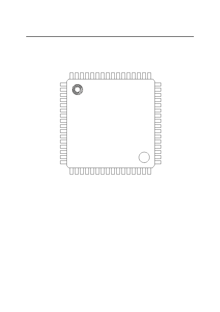
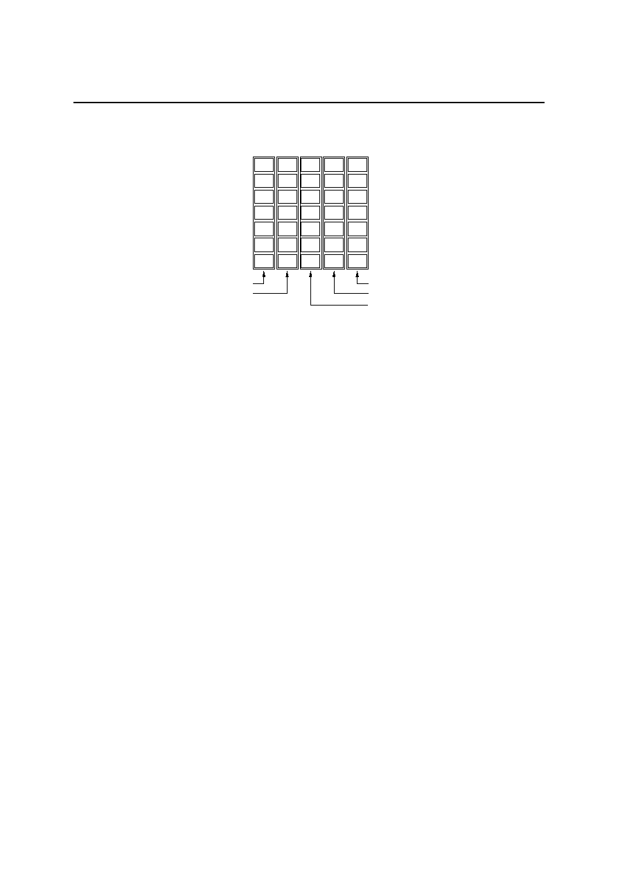
PIN CONFIGURATION (TOP VIEW)
64-Pin Plastic QFP
1
2
3
4
5
6
7
8
9
10
11
12
13
14
15
16
SEG5
SEG6
SEG7
SEG8
SEG9
SEG10
SEG11
SEG12
SEG13
SEG14
SEG15
SEG16
SEG17
SEG18
SEG19
SEG20
17
18
19
20
21
22
23
24
25
26
27
28
29
30
31
32
SEG21
SEG22
SEG23
SEG24
SEG25
SEG26
SEG27
SEG28
SEG29
SEG30
SEG31
SEG32
SEG33
SEG34
SEG35
COM1
48
47
46
45
44
43
42
41
40
39
38
37
36
35
34
33
V
FL
COM16
COM15
COM14
COM13
COM12
COM11
COM10
COM9
COM8
COM7
COM6
COM5
COM4
COM3
COM2
64
63
62
61
60
59
58
57
56
55
54
53
52
51
50
49
SEG4
SEG3
SEG2
SEG1
AD1
AD2
P2
P1
V
DD
DA
CP
C
S
R
ESET
OSC1
OSC0
GND
FEDL9208-01
OKI Semiconductor
ML9208
4/33
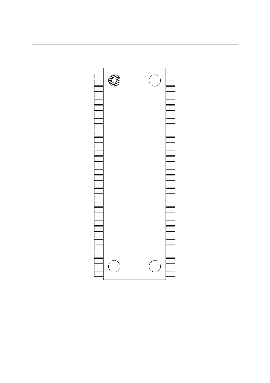
64-Pin Plastic SSOP
20
1
2
3
4
5
6
7
8
9
10
11
12
13
14
15
16
17
18
19
21
22
23
24
25
26
27
28
29
30
31
32
45
64
63
62
61
60
59
58
57
56
55
54
53
52
51
50
49
48
47
46
44
43
42
41
40
39
38
37
36
35
34
33
SEG16
P1
P2
AD2
AD1
SEG1
SEG2
SEG3
SEG4
SEG5
SEG6
SEG7
SEG8
SEG9
SEG10
SEG11
SEG12
SEG13
SEG14
SEG15
SEG17
SEG18
SEG19
SEG20
SEG21
SEG22
SEG23
SEG24
SEG25
SEG26
SEG27
SEG28
COM6
V
DD
DA
CP
CS
RESET
OSC1
OSC0
GND
V
FL
COM16
COM15
COM14
COM13
COM12
COM11
COM10
COM9
COM8
COM7
COM5
COM4
COM3
COM2
COM1
SEG35
SEG34
SEG33
SEG32
SEG31
SEG30
SEG29

FEDL9208-01
OKI Semiconductor
ML9208
5/33
PIN DESCRIPTION
Pin
QFP SSOP
Symbol Type Connects
to
Description
1 to 31,
61 to 64
5 to 39 SEG1 to 35 O
Fluorescent
tube anode
electrode
Fluorescent display tube anode electrode drive output.
Directly connected to fluorescent display tube and a
pull-down resistor is not necessary. I
OH
> ≠6 mA
32 to 47 40 to 55 COM1 to 16 O
Fluorescent
tube grid
electrode
Fluorescent display tube grid electrode drive output.
Directly connected to fluorescent display tube and a
pull-down resistor is not necessary. I
OH
> ≠30 mA
59, 60
3, 4
AD1, AD2
O
Fluorescent
tube anode
electrode
Fluorescent display tube anode electrode drive output.
Directly connected to fluorescent display tube and a
pull-down resistor is not necessary. I
OH
> ≠15 mA
57, 58
1, 2
P1, P2
O
LED drive
control pins
General port output.
Output of these pins in static operation, so these pins can
drive the LED.
56 64 V
DD
49 57 GND
48 56 V
FL
-- Power
supply
V
DD
-GND are power supplies for internal logic.
V
DD
-V
FL
are power supplies for driving fluorescent tubes.
Apply V
FL
after V
DD
is applied.
55 63 DA I
Microcontroller
Serial data input (positive logic).
Input from LSB.
54 62
CP
I Microcontroller
Shift clock input.
Serial data is shifted on the rising edge of
CP
.
53 61
CS
I Microcontroller
Chip select input.
Serial data transfer is disabled when
CS
pin is "H" level.
Reset input.
"Low" initializes all the functions.
Initial status is as follows.
∑
Address of each RAM
address "00"H
∑
Data of each RAM
Content is undefined
∑
Display digit
16 digits
∑
Contrast adjustment
8/16
∑
All lights ON or OFF
OFF mode
∑
All outputs
"Low" level
52 60
RESET
I
Microcontroller
or C
2
, R
2
(Circuit when R and C are
connected externally)
See Application Circuit.
50 58 OSC0 I
External RC pin for RC oscillation.
Connect R and C externally. The RC time constant
depends on the V
DD
voltage used. Set the target oscillation
frequency to 2 MHz.
51 59 OSC1 O
C
1
, R
1
(RC oscillation circuit)
See Application Circuit.
OSC0
OSC1
R
1
C
1
RESET
R
2
C
2

FEDL9208-01
OKI Semiconductor
ML9208
6/33
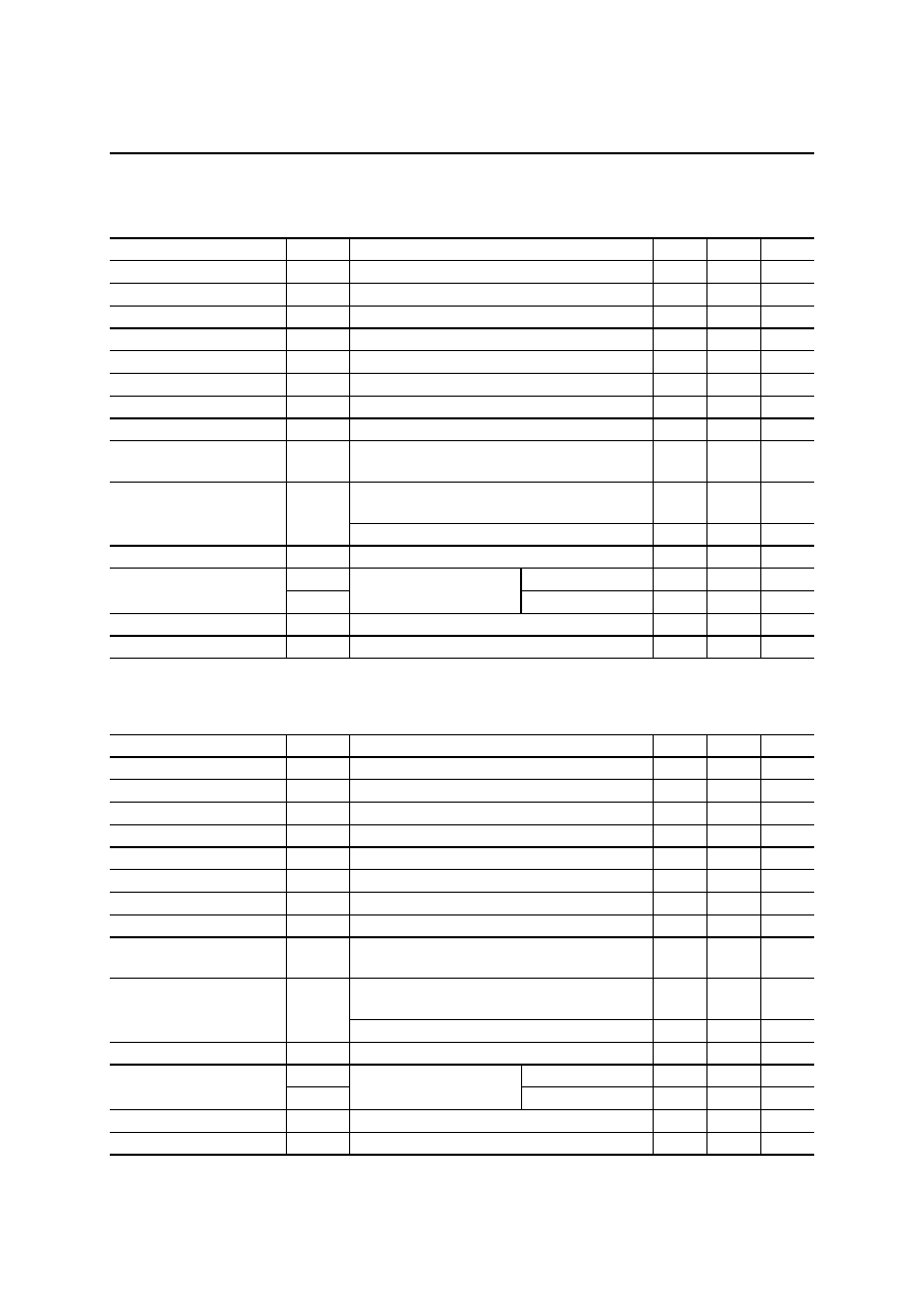
ABSOLUTE MAXIMUM RATINGS
Parameter Symbol
Condition
Rating Unit
Supply Voltage (1)
V
DD
--
≠0.3 to 6.5
V
Supply Voltage (2)
V
FL
--
≠45 to V
DD
+0.3
V
Input Voltage
V
IN
--
≠0.3 to V
DD
+0.3
V
QFP 541
Power Dissipation
P
D
Ta
25
∞
C
SSOP 590
mW
Storage Temperature
T
STG
--
≠55 to 150
∞
C
I
O1
COM1 to 16
≠40 to 0.0
mA
I
O2
AD1, AD2
≠20 to 0.0
mA
I
O3
SEG1 to 35
≠10 to 0.0
mA
Output Current
I
O4
P1, P2
≠4.0 to 4.0
mA
RECOMMENDED OPERATING CONDITIONS-1
When the power supply voltage is 5 V (typ.)
Parameter Symbol
Condition
Min.
Typ.
Max.
Unit
Supply Voltage (1)
V
DD
-- 4.5
5.0
5.5
V
Supply Voltage (2)
V
FL
--
≠36.5
--
≠20
V
High Level Input Voltage
V
IH
All input pins excluding OSC0 pin
0.7 V
DD
--
--
V
Low Level Input Voltage
V
IL
All input pins excluding OSC0 pin
--
--
0.3 V
DD
V
CP
Frequency
f
C
-- --
--
2.0
MHz
Oscillation Frequency
f
OSC
R
1
= 3.3 k
, C
1
= 39 pF
1.5
2.0
2.5
MHz
Frame Frequency
f
FR
DIGIT = 1 to 16, R
1
= 3.3 k
, C
1
= 39 pF 183
244
305
Hz
Operating Temperature
T
op
-- ≠40
--
85
∞
C
FEDL9208-01
OKI Semiconductor
ML9208
7/33
RECOMMENDED OPERATING CONDITIONS-2
When the power supply voltage is 3.3 V (typ.)
Parameter Symbol
Condition
Min.
Typ.
Max.
Unit
Supply Voltage (1)
V
DD
--
3.0 3.3 3.6 V
Supply Voltage (2)
V
FL
--
≠38.4
--
≠20
V
High Level Input Voltage
V
IH
All input pins excluding OSC0 pin
0.8 V
DD
--
--
V
Low Level Input Voltage
V
IL
All input pins excluding OSC0 pin
--
--
0.2 V
DD
V
CP
Frequency
f
C
-- --
--
2.0
MHz
Oscillation Frequency
f
OSC
R
1
= 3.3 k
, C
1
= 39 pF
1.5
2.0
2.5
MHz
Frame Frequency
f
FR
DIGIT = 1 to 16, R
1
= 3.3 k
, C
1
= 39 pF 183
244
305
Hz
Operating Temperature
T
op
-- ≠40
--
85
∞
C
ELECTRICAL CHARACTERISTICS
DC Characteristics-1
(V
DD
= 5.0 V
±
10%, V
FL
= V
DD
≠42 V, Ta = ≠40 to +85
∞
C, unless otherwise specified)
Parameter Symbol
Applied
pin
Condition
Min.
Max.
Unit
High Level Input Voltage
V
IH
CS
,
CP
, DA,
RESET
-- 0.7
V
DD
--
V
Low Level Input Voltage
V
IL
CS
,
CP
, DA,
RESET
-- --
0.3
V
DD
V
High Level Input Current
I
IH
CS
,
CP
, DA,
RESET
V
IH
= V
DD
≠1.0
1.0
µA
Low Level Input Current
I
IL
CS
,
CP
, DA,
RESET
V
IL
= 0.0 V
≠1.0
1.0
µA
V
OH1
COM1 to 16
I
OH1
= ≠30 mA
V
DD
≠1.5
--
V
V
OH2
AD1,
AD2
I
OH2
= ≠15 mA
V
DD
≠1.5
--
V
V
OH3
SEG1 to 35
I
OH3
= ≠6 mA
V
DD
≠1.5
--
V
High Level Output Voltage
V
OH4
P1,
P2
I
OH4
= ≠2 mA
V
DD
≠1.0
--
V
V
OL1
COM1 to 16
AD1, AD2
SEG1 to 35
-- --
V
FL
+1.0
V
Low Level Output Voltage
V
OL2
P1,
P2
I
OL1
= 2 mA
--
1.0
V
I
DD1
Duty = 15/16
Digit = 1 to 16
All output lights ON
-- 4 mA
Current Consumption
I
DD2
V
DD
f
OSC
=
2 MHz,
no load
Duty = 8/16
Digit = 1 to 9
All output lights OFF
-- 3 mA
FEDL9208-01
OKI Semiconductor
ML9208
8/33
DC Characteristics-2
(V
DD
= 3.3 V
±
10%, V
FL
= V
DD
≠42 V, Ta = ≠40 to +85
∞
C, unless otherwise specified)
Parameter Symbol
Applied
pin
Condition
Min.
Max.
Unit
High Level Input Voltage
V
IH
CS
,
CP
,
DA,
RESET
-- 0.8
V
DD
--
V
Low Level Input Voltage
V
IL
CS
,
CP
,
DA,
RESET
-- --
0.2
V
DD
V
High Level Input Current
I
IH
CS
,
CP
,
DA,
RESET
V
IH
= V
DD
≠1.0
1.0
µA
Low Level Input Current
I
IL
CS
,
CP
,
DA,
RESET
V
IL
= 0.0 V
≠1.0
1.0
µA
V
OH1
COM1 to 16
I
OH1
= ≠30 mA
V
DD
≠1.5
--
V
V
OH2
AD1,
AD2
I
OH2
= ≠15 mA
V
DD
≠1.5
--
V
V
OH3
SEG1 to 35
I
OH3
= ≠6 mA
V
DD
≠1.5
--
V
High Level Output Voltage
V
OH4
P1,
P2
I
OH4
= ≠1 mA
V
DD
≠1.0
--
V
V
OL1
COM1 to 16
AD1, AD2
SEG1 to 35
-- --
V
FL
+1.0
V
Low Level Output Voltage
V
OL2
P1,
P2
I
OL1
= 1 mA
--
1.0
V
I
DD1
Duty = 15/16
Digit = 1 to 16
All output lights ON
-- 3 mA
Current Consumption
I
DD2
V
DD
F
OSC
=
2 MHz,
no load
Duty = 8/16
Digit = 1 to 9
All output lights OFF
-- 2 mA
FEDL9208-01
OKI Semiconductor
ML9208
9/33
AC Characteristics-1
(V
DD
= 5.0 V
±
10%, V
FL
= V
DD
≠42 V, Ta = ≠40 to +85
∞
C, unless otherwise specified)
Parameter Symbol
Condition
Min.
Max.
Unit
CP
Frequency
f
C
-- --
2.0
MHz
CP
Pulse Width
t
CW
-- 250
--
ns
DA Setup Time
t
DS
-- 250
--
ns
DA Hold Time
t
DH
-- 250
--
ns
CS
Setup Time
t
CSS
-- 250
--
ns
CS
Hold Time
t
CSH
R
1
= 3.3 k
, C
1
= 47 pF
16
--
µ
s
CS
Wait Time
t
CSW
-- 250
--
ns
Data Processing Time
t
DOFF
R
1
= 3.3 k
, C
1
= 47 pF
8
--
µ
s
RESET
Pulse Width
t
WRES
When
RESET
signal is input from
microcontroller etc. externally
250 -- ns
When
RESET
signal is input from
microcontroller etc. externally
250 -- ns
RESET
Time
t
RSON
R
2
= 1.0 k
, C
2
= 0.1
µ
F --
200
µ
s
DA Wait Time
t
RSOFF
-- 250
--
ns
t
R
t
R
= 20 to 80%
--
2.0
µ
s
All Output Slew Rate
t
F
C
l
= 100 pF
t
F
= 80 to 20%
--
2.0
µ
s
V
DD
Rise Time
t
PRZ
When mounted in the unit
--
100
µ
s
V
DD
Off Time
t
POF
When mounted in the unit, V
DD
= 0.0 V
5.0
--
ms
AC Characteristics-2
(V
DD
= 3.3 V
±
10%, V
FL
= V
DD
≠42 V, Ta = ≠40 to +85
∞
C, unless otherwise specified)
Parameter Symbol
Condition
Min.
Max.
Unit
CP
Frequency
f
C
-- --
2.0
MHz
CP
Pulse Width
t
CW
-- 250
--
ns
DA Setup Time
t
DS
-- 250
--
ns
DA Hold Time
t
DH
-- 250
--
ns
CS
Setup Time
t
CSS
-- 250
--
ns
CS
Hold Time
t
CSH
R
1
= 3.3 k
, C
1
= 39 pF
16
--
µ
s
CS
Wait Time
t
CSW
-- 250
--
ns
Data Processing Time
t
DOFF
R
1
= 3.3 k
, C
1
= 39 pF
8
--
µ
s
RESET
Pulse Width
t
WRES
When
RESET
signal is input from
microcontroller etc. externally
250 -- ns
When
RESET
signal is input from
microcontroller etc. externally
250 -- ns
RESET
Time
t
RSON
R
2
= 1.0 k
, C
2
= 0.1
µ
F --
200
µ
s
DA Wait Time
t
RSOFF
-- 250
--
ns
t
R
t
R
= 20 to 80%
--
2.0
µ
s
All Output Slew Rate
t
F
C
l
= 100 pF
t
F
= 80 to 20%
--
2.0
µ
s
V
DD
Rise Time
t
PRZ
When mounted in the unit
--
100
µ
s
V
DD
Off Time
t
POF
When mounted in the unit, V
DD
= 0.0 V
5.0
--
ms
FEDL9208-01
OKI Semiconductor
ML9208
10/33
TIMING DIAGRAM
Symbol V
DD
= 3.3 V
±
10% V
DD
= 5.0 V
±
10%
V
IH
0.8
V
DD
0.7
V
DD
V
IL
0.2
V
DD
0.3
V
DD
∑ Data Timing
∑ Reset Timing
∑ Output Timing
CS
CP
DA
t
CSS
t
DS
t
DH
t
DOFF
t
CW
t
CW
t
CSH
t
CSW
VALID
VALID
VALID
VALID
V
IH
V
IH
f
C
V
IL
V
IL
V
IH
V
IL
V
DD
RESET
DA
t
PRZ
t
RSON
t
RSOFF
t
POF
t
WRES
When external
R and C are
connected
When input externally
0.8 V
DD
V
IH
0.0 V
V
IL
V
IH
V
IL
0.5 V
DD
t
RSOFF
=
All outputs
t
F
t
R
0.8 V
DD
0.2 V
FL
FEDL9208-01
OKI Semiconductor
ML9208
11/33
∑ Digit Output Timing (for 16-digit display, at a duty of 15/16)
AD1, 2
SEG1-35
COM1
COM2
COM3
COM4
COM5
COM6
COM7
COM8
COM9
COM10
COM11
COM12
COM13
COM14
COM15
COM16
V
FL
t
1
= 1024T
t
2
= 60T
t
3
= 4T
Frame cycle
Display timing
Blank timing
V
DD
V
FL
V
DD
T = 8/f
OSC
(t
1
= 4.096 ms when f
osc
= 2.0 MHz)
(t
2
= 240
µ
s when f
osc
= 2.0 MHz)
(t
3
= 16
µ
s when f
osc
= 2.0 MHz)
FEDL9208-01
OKI Semiconductor
ML9208
12/33
FUNCTIONAL DESCRIPTION
Commands List
Command
LSB
1st
byte
MSB LSB
2nd
byte
MSB
B0 B1 B2 B3 B4 B5 B6 B7 B0 B1 B2 B3 B4 B5 B6 B7
1 DCRAM data write
X0 X1 X2 X3 1 0 0 0 C0 C1 C2 C3 C4 C5 C6 C7
C0 C5 C10 C15 C20 C25 C30 *
2nd byte
C1 C6 C11 C16 C21 C26 C31 *
3rd byte
C2 C7 C12 C17 C22 C27 C32 *
4th byte
C3 C8 C13 C18 C23 C28 C33 *
5th byte
2 CGRAM data write
X0 X1 X2 *
0
1
0
0
C4 C9 C14 C19 C24 C29 C34 *
6th byte
3
ADRAM
data
write
X0
X1
X2
X3 1 1 0 0 C0
C1 * * * * * *
4 General output port set P1 P2 *
*
0
0
1
0
5 Display duty set
D0 D1 D2 *
1
0
1
0
6 Number of digits set
K0 K1 K2 *
0
1
1
0
7 All lights ON/OFF
L H
*
*
1
1
1
0
Test
mode
*: Don't
care
Xn: Address specification for each RAM
Cn: Character code specification for each
RAM
Pn: General output port status
specification
Dn: Display duty specification
Kn: Number of digits specification
H: All lights ON instruction
L: All lights OFF instruction
When data is written to RAM (DCRAM, CGRAM, ADRAM) continuously, addresses are internally incremented
automatically.
Therefore it is not necessary to specify the 1st byte to write RAM data for the 2nd and later bytes.
Note: The test mode is used for inspection before shipment. It is not a user function.
FEDL9208-01
OKI Semiconductor
ML9208
13/33
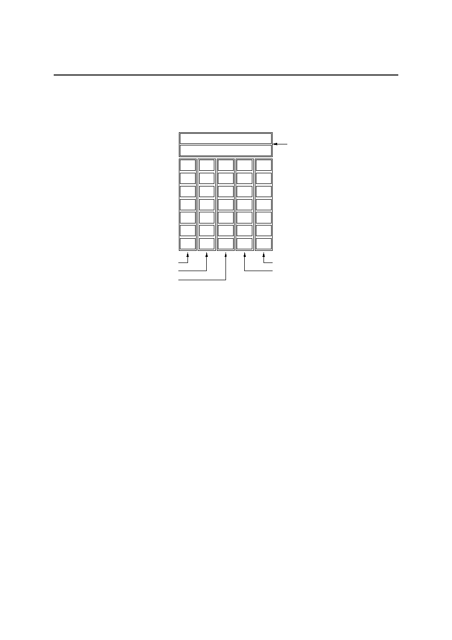
Positional Relationship Between SEGn and ADn (one digit)
C0 AD1
C0
SEG1
C5
SEG6
C10
SEG11
C15
SEG16
C20
SEG21
C25
SEG26
C30
SEG31
C1
SEG2
C6
SEG7
C11
SEG12
C16
SEG17
C21
SEG22
C26
SEG27
C31
SEG32
C2
SEG3
C7
SEG8
C12
SEG13
C17
SEG18
C22
SEG23
C27
SEG28
C32
SEG33
C3
SEG4
C8
SEG9
C13
SEG14
C18
SEG19
C23
SEG24
C28
SEG29
C33
SEG34
C4
SEG5
C9
SEG10
C14
SEG15
C19
SEG20
C24
SEG25
C29
SEG30
C34
SEG35
ADRAM written data.
Corresponds to 2nd byte
CGRAM written data. Corresponds to 2nd byte
CGRAM written data. Corresponds to 3rd byte
CGRAM written data. Corresponds to 4th byte
CGRAM written data. Corresponds to 6th byte
CGRAM written data. Corresponds to 5th byte
C1 AD2

FEDL9208-01
OKI Semiconductor
ML9208
14/33
Data Transfer Method and Command Write Method
Display control command and data are written by an 8-bit serial transfer.
Write timing is shown in the figure below.
Setting the
CS pin to "Low" level enables a data transfer.
Data is 8 bits and is sequentially input into the DA pin from LSB (LSB first).
As shown in the figure below, data is read by the shift register at the rising edge of the shift clock, which is input
into the
CP pin. If 8-bit data is input, internal load signals are automatically generated and data is written to each
register and RAM.
Therefore it is not necessary to input load signals from the outside.
Setting the
CS pin to "High" disables data transfer. Data input from the point when the CS pin changes from
"High" to "Low" is recognized in 8-bit units.
t
DOFF
B0
LSB
CS
CP
DA
B1
B2
B3
B4
B5
B6
B7
B0
B1
B2
B3
B4
B5
B6
B7
MSB
1st byte
LSB
MSB
2nd byte
When data is written
to DCRAM*
Command and address
data
t
CSH
B0
B1
B2
B3
B4
B5
B6
B7
LSB
MSB
2nd byte
Character code data of
the next address
Character code data
* When data is written to RAM (DCRAM, ADRAM, CGRAM) continuously, addresses are internally
incremented automatically.
Therefore it is not necessary to specify the 1st byte to write RAM data for the 2nd and later bytes.
Reset Function
Reset is executed when the
RESET pin is set to "L", (when turning power on, for example) and initializes all
functions.
Initial status is as follows.
∑ Address of each RAM address "00"H
∑ Data of each RAM All contents are undefined
∑ General output port All general output ports go "Low"
∑ Display digit 16 digits
∑ Contrast adjustment 8/16
∑ All display lights ON or OFF OFF mode
∑ Segment output All segment outputs go "Low"
∑ AD output All AD outputs go "Low"
Please set again according to "Setting Flowchart" after reset.
FEDL9208-01
OKI Semiconductor
ML9208
15/33
Description of Commands and Functions
1. DCRAM data write
(Specifies the address of DCRAM and writes the character code of CGROM and CGRAM.)
DCRAM (Data Control RAM) has a 4-bit address to store character code of CGROM and CGRAM.
The character code specified by DCRAM is converted to a 5
◊ 7 dot matrix character pattern via CGROM or
CGRAM.
(The DCRAM can store 16 characters.)
[Command format]
X0
X1
X2
X3
1
0
0
0
B0
B1
B2
B3
B4
B5
B6
B7
1st byte
(1st)
LSB
MSB
C0
C1
C2
C3
C4
C5
C6
C7
B0
B1
B2
B3
B4
B5
B6
B7
2nd byte
(2nd)
LSB
MSB
:
selects DCRAM data write mode and specifies DCRAM
address
(Ex: Specifies DCRAM address 0H)
:
specifies character code of CGROM and CGRAM
(written into DCRAM address 0H)
To specify the character code of CGROM and CGRAM continuously to the next address, specify only character
code as follows.
The addresses of DCRAM are automatically incremented. Specification of an address is unnecessary.
FEDL9208-01
OKI Semiconductor
ML9208
16/33
C0
C1
C2
C3
C4
C5
C6
C7
B0
B1
B2
B3
B4
B5
B6
B7
2nd byte
(3rd)
LSB
MSB
C0
C1
C2
C3
C4
C5
C6
C7
B0
B1
B2
B3
B4
B5
B6
B7
2nd byte
(4th)
LSB
MSB
:
specifies character code of CGROM and CGRAM
(written into DCRAM address 1H)
:
specifies character code of CGROM and CGRAM
(written into DCRAM address 2H)
B0
B1
B2
B3
B4
B5
B6
B7
2nd byte
(17th)
LSB
MSB
C0
C1
C2
C3
C4
C5
C6
C7
B0
B1
B2
B3
B4
B5
B6
B7
2nd byte
(18th)
LSB
MSB
:
specifies character code of CGROM and CGRAM
(written into DCRAM address FH)
:
specifies character code of CGROM and CGRAM
(DCRAM address 0H is rewritten)
C0
C1
C2
C3
C4
C5
C6
C7
X0 (LSB) to X3 (MSB) : DCRAM addresses (4 bits: 16 characters)
C0 (LSB) to C7 (MSB) : Character code of CGROM and CGRAM (8 bits: 256 characters)
[COM positions and set DCRAM addresses]
HEX X0 X1 X2 X3
COM
position
0 0 0 0 0 COM1
1 1 0 0 0 COM2
2 0 1 0 0 COM3
3 1 1 1 0 COM4
4 0 0 1 0 COM5
5 1 0 1 0 COM6
6 0 1 1 0 COM7
7 1 1 1 0 COM8
8 0 0 0 1 COM9
9 1 0 0 1 COM10
A 0 1 0 1 COM11
B 1 1 0 1 COM12
C 0 0 1 1 COM13
D 1 0 1 1 COM14
E 0 1 1 1 COM15
F 1 1 1 1 COM16
FEDL9208-01
OKI Semiconductor
ML9208
17/33
2. CGRAM data write
(Specifies the addresses of CGRAM and writes character pattern data.)
CGRAM (Character Generator RAM) has a 3-bit address to store 5
◊ 7 dot matrix character patterns.
A character pattern stored in CGRAM can be displayed by specifying the character code (address) by
DCRAM.
The address of CGRAM is assigned to 00H to 07H. (All the other addresses are the CGROM addresses.)
(The CGRAM can store 8 types of character patterns.)
[Command format]
C0
C5
C10
C15
C20
C25
C30
*
B0
B1
B2
B3
B4
B5
B6
B7
2nd byte
(2nd)
LSB
MSB
:
specifies 1st column data
(rewritten into CGRAM address 00H)
C1
C6
C11
C16
C21
C26
C31
*
B0
B1
B2
B3
B4
B5
B6
B7
3rd byte
(3rd)
LSB
MSB
:
specifies 2nd column data
(rewritten into CGRAM address 00H)
X0
X1
X2
*
0
1
0
0
B0
B1
B2
B3
B4
B5
B6
B7
1st byte
(1st)
LSB
MSB
:
selects CGRAM data write mode and specifies
CGRAM address.
(Ex: specifies CGRAM address 00H)
C2
C7
C12
C17
C22
C27
C32
*
B0
B1
B2
B3
B4
B5
B6
B7
4th byte
(4th)
LSB
MSB
:
specifies 3rd column data
(rewritten into CGRAM address 00H)
C3
C8
C13
C18
C23
C28
C33
*
B0
B1
B2
B3
B4
B5
B6
B7
5th byte
(5th)
LSB
MSB
:
specifies 4th column data
(rewritten into CGRAM address 00H)
C4
C9
C14
C19
C24
C29
C34
*
B0
B1
B2
B3
B4
B5
B6
B7
6th byte
(6th)
LSB
MSB
:
specifies 5th column data
(rewritten into CGRAM address 00H)
To specify character pattern data continuously to the next address, specify only character pattern data as
follows.
The addresses of CGRAM are automatically incremented. Specification of an address is therefore
unnecessary.
The 2nd to 6th byte (character pattern data) are regarded as one data item, so 250 ns is sufficient for t
DOFF
time
between bytes.
FEDL9208-01
OKI Semiconductor
ML9208
18/33
C0
C5
C10
C15
C20
C25
C30
*
B0
B1
B2
B3
B4
B5
B6
B7
2nd byte
(7th)
LSB
MSB
:
specifies 1st column data
(rewritten into CGRAM address 01H)
C4
C9
C14
C19
C24
C29
C34
*
B0
B1
B2
B3
B4
B5
B6
B7
6th byte
(11th)
LSB
MSB
:
specifies 5th column data
(rewritten into CGRAM address 01H)
X0 (LSB) to X2 (MSB) : CGRAM addresses (3 bits: 8 characters)
C0 (LSB) to C34 (MSB) : Character pattern data (35 bits: 35 outputs per digit)
* : Don't care
[CGROM addresses and set CGRAM addresses]
Refer to ROMCODE table
HEX X0 X1 X2 CGROM
address
00 0 0 0 RAM00(00000000B)
01 1 0 0 RAM01(00000001B)
02 0 1 0 RAM02(00000010B)
03 1 1 0 RAM03(00000011B)
04 0 0 1 RAM04(00000100B)
05 1 0 1 RAM05(00000101B)
06 0 1 1 RAM06(00000110B)
07 1 1 1 RAM07(00000111B)
FEDL9208-01
OKI Semiconductor
ML9208
19/33
Positional relationship between the output area of CGROM and that of CGRAM
C0
C5
C10
C15
C20
C25
C30
C1
C6
C11
C16
C21
C26
C31
C2
C7
C12
C17
C22
C27
C32
C3
C8
C13
C18
C23
C28
C33
C4
C9
C14
C19
C24
C29
C34
area that corresponds to 2nd byte (1st column)
area that corresponds to 3rd byte (2nd column)
area that corresponds to 5th byte (4th column)
area that corresponds to 6th byte (5th column)
area that corresponds to 4th byte (3rd column)
Note: CGROM (Character Generator ROM) has an 8-bit address to generate 5
◊ 7 dot matrix character patterns.
CGRAM can store 248 types of character patterns.
FEDL9208-01
OKI Semiconductor
ML9208
20/33
3. ADRAM data write
(specifies address of ADRAM and writes symbol data)
ADRAM (Additional Data RAM) has a 2-bit address to store symbol data.
Symbol data specified by ADRAM is directly output without CGROM and CGRAM.
(The ADRAM can store 2 types of symbol patterns for each digit.)
The terminal to which the contents of ADRAM are output can be used as a cursor.
[Command format]
C0
C1
*
*
*
*
*
*
B0
B1
B2
B3
B4
B5
B6
B7
2nd byte
(2nd)
LSB
MSB
:
sets symbol data
(written into ADRAM address 0H)
X0
X1
X2
X3
1
1
0
0
B0
B1
B2
B3
B4
B5
B6
B7
1st byte
(1st)
LSB
MSB
:
selects ADRAM data write mode and specifies ADRAM
address
(Ex: specifies ADRAM address 0H)
To specify symbol data continuously to the next address, specify only symbol data as follows.
The address of ADRAM is automatically incremented. Specification of addresses is therefore unnecessary.
C0
C1
*
*
*
*
*
*
B0
B1
B2
B3
B4
B5
B6
B7
2nd byte
(3rd)
LSB
MSB
:
sets symbol data
(written into ADRAM address 1H)
C0
C1
*
*
*
*
*
*
B0
B1
B2
B3
B4
B5
B6
B7
2nd byte
(4th)
LSB
MSB
:
sets symbol data
(written into ADRAM address 2H)
C0
C1
*
*
*
*
*
*
B0
B1
B2
B3
B4
B5
B6
B7
2nd byte
(17th)
LSB
MSB
:
sets symbol data
(written into ADRAM address FH)
C0
C1
*
*
*
*
*
*
B0
B1
B2
B3
B4
B5
B6
B7
2nd byte
(18th)
LSB
MSB
:
sets symbol data
(ADRAM address 0H is rewritten.)
X0 (LSB) to X3 (MSB) : ADRAM addresses (4 bits: 16 characters)
C0 (LSB) to C1 (MSB) : Symbol data (2 bits: 2-symbol data per digit)
* : Don't care
FEDL9208-01
OKI Semiconductor
ML9208
21/33
[COM positions and ADRAM addresses]
HEX X0 X1 X2 X3 COM
position
0 0 0 0 0
COM1
1 1 0 0 0
COM2
2 0 1 0 0
COM3
3 1 1 1 0
COM4
4 0 0 1 0
COM5
5 1 0 1 0
COM6
6 0 1 1 0
COM7
7 1 1 1 0
COM8
8 0 0 0 1
COM9
9 1 0 0 1
COM10
A 0 1 0 1
COM11
B 1 1 0 1
COM12
C 0 0 1 1
COM13
D 1 0 1 1
COM14
E 0 1 1 1
COM15
F 1 1 1 1
COM16
4. General output port set
(specifies the general output port status)
The general output port is an output for 2-bit static operation.
It is used to control other I/O devices and turn on LED. (static operation)
When at the "High" level, this output becomes the V
DD
voltage, and when at the "Low" level, it becomes the
ground potential. Therefore, the fluorescent display tube cannot be driven.
[Command format]
P1
P2
*
*
0
0
1
0
B0
B1
B2
B3
B4
B5
B6
B7
1st byte
LSB
MSB
:
selects a general output port and specifies
the output status
P1, P2 : general output port
* : don't care
[Set data and set state of general output port]
P1
P2
Display state of general output port
0
0
Sets P1 and P2 to low
1
0
Sets P1 to high and P2 to low
(The state when power is applied or when
RESET
is
input.)
0
1
Sets P1 to low and P2 to high
1
1
Sets P1 and P2 to high
FEDL9208-01
OKI Semiconductor
ML9208
22/33
5. Display duty set
(writes display duty value to duty cycle register)
Display duty adjusts contrast in 8 stages using 3-bit data.
When power is turned on or when the
RESET signal is input, the duty cycle register value is "0". Always
execute this instruction before turning the display on, then set a desired duty value.
[Command format]
D0
D1
D2
*
1
0
1
0
B0
B1
B2
B3
B4
B5
B6
B7
1st byte
LSB
MSB
:
selects display duty set mode and sets duty value
D0 (LSB) to D2 (MSB) : display duty data (3 bits: 8 stages)
* : don't care
[Relation between setup data and controlled COM duty]
HEX D0 D1 D2 COM
duty
0 0 0 0 8/16
1 1 0 0 9/16
(The state when power is turned on or when
RESET
signal
is input.)
2 0 1 0 10/16
3 1 1 0 11/16
4 0 0 1 12/16
5 1 0 1 13/16
6 0 1 1 14/16
7 1 1 1 15/16
FEDL9208-01
OKI Semiconductor
ML9208
23/33
6. Number of digits set
(writes the number of display digits to the display digit register)
The number of digits set can display 9 to 16 digits using 3-bit data.
When power is turned on or when a
RESET signal is input, the number of digit register value is "0". Always
execute this instruction to change the number of digits before turning the dispaly on.
[Command format]
K0
K1
K2
*
0
1
1
0
B0
B1
B2
B3
B4
B5
B6
B7
1st byte
LSB
MSB
:
selects the number of digit set mode and specifies
the number of digit value
K0 (LSB) to K2 (MSB) : number of digit data (3 bits: 8 digits)
* : don't care
[Relation between setup data and controlled COM]
HEX K0 K1 K2
Number of digits of
COM
0
0
0
0
COM1 to 16
1
1
0
0
COM1 to 9
(The state when power is turned on or when
RESET
signal is input.)
2
0
1
0
COM1 to 10
3
1
1
0
COM1 to 11
4
0
0
1
COM1 to 12
5
1
0
1
COM1 to 13
6
0
1
1
COM1 to 14
7
1
1
1
COM1 to 15

FEDL9208-01
OKI Semiconductor
ML9208
24/33
7. All display lights ON/OFF set
(turns all dispaly lights ON or OFF)
All display lights ON is used primarily for display testing.
All display lights OFF is primarily used for display blink and to prevent malfunction when power is turned on.
This command cannot control the general output port.
[Command format]
L
H
*
*
1
1
1
0
B0
B1
B2
B3
B4
B5
B6
B7
1st byte
LSB
MSB
:
selects all display lights ON or OFF mode
L: sets all lights OFF
H: sets all lights ON
*: Don't care
[Set data and display state of SEG and AD]
L
H
Display state of SEG and AD
0 0
Normal
display
1
0
Sets all outputs to Low
(The state when power is applied or when
RESET
is input.)
0
1
Sets all outputs to High
1
1
Sets all outputs to High
(All lights ON mode has priority.)
FEDL9208-01
OKI Semiconductor
ML9208
25/33
Setting Flowchart
(Power applying included)
Apply V
FL
All display lights OFF
Number of digits setting
Display duty setting
CGRAM
Data write mode
(with address setting)
CGRAM
Character code
CGRAM
Is character code
write ended?
Another RAM to
be set?
General output port setting
Releases all display lights
OFF mode
ADRAM
Data write mode
(with address setting)
ADRAM
Character code
ADRAM
Is character code
write ended?
DCRAM
Data write mode
(with address setting)
DCRAM
Character code
DCRAM
Is character code
write ended?
Select a RAM to be used
Status of all outputs by
RESET
signal input
Display operation mode
Address is automatically
incremented
NO
NO
NO
YES
YES
YES
YES
End
Address is automatically
incremented
Address is automatically
incremented
Apply V
DD
NO
FEDL9208-01
OKI Semiconductor
ML9208
26/33
Power-off Flowchart
Display operation mode
Turn off V
DD
Turn off V
FL
FEDL9208-01
OKI Semiconductor
ML9208
27/33
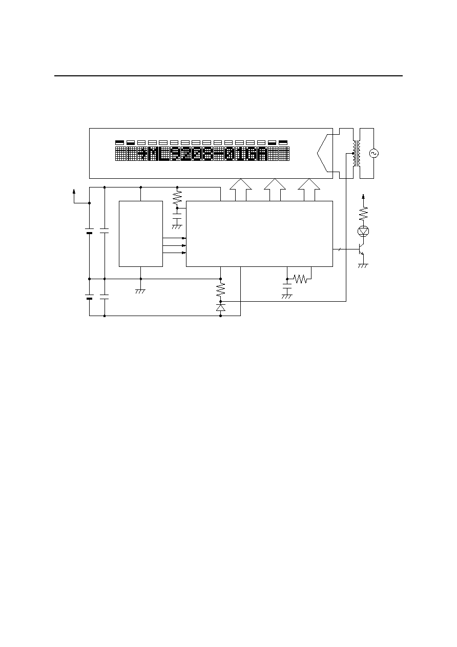
APPLICATION CIRCUIT
ML9208-01
Micro-
controller
16
35
2
RESET
V
DD
COM1 to 16
SEG1 to 35
AD1, 2
V
DD
GND
R
2
C
2
GND
R
1
C
1
V
FL
OSC0
OSC1
DA
CP
CS
Output Port
P1, 2
R
3
C
3
C
4
V
DD
V
FL
ZD
2
5
◊
7-dot matrix fluorescent display tube
GRID
(DIGIT)
ANODE
(SEGMENT)
ANODE
(SEGMENT)
Heater Transformer
R
4
LED
V
DD
NPN Tr
GND
GND
GND
V
DD
Notes: 1. The V
DD
value depends on the power supply voltage of the microcontroller used. Adjust the values of
the constants R
1
, R
2
, R
4
, C
1
, and C
2
to the power supply voltage used.
2.
The
V
FL
value depends on the fluorescent display tube used. Adjust the values of the constants R
3
and
ZD to the power supply voltage used.

FEDL9208-01
OKI Semiconductor
ML9208
28/33
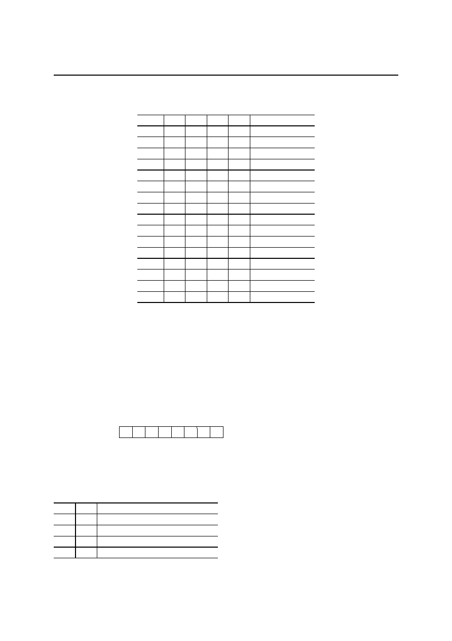
Reference data
The figure below shows the relationship between the V
FL
voltage and the output current of each driver.
Take care that the total power consumption to be used does not exceed the power dissipation.
≠30
≠25
≠20
≠15
≠10
≠5
0
≠17
≠22
≠27
≠32
≠37
≠42
Output Current (m
A)
V
FL
Voltage (V
DD ≠ n
)
COM1 to 16
(Condition: V
OH
= V
DD
≠ 1.5 V)
AD1 and AD2
(Condition: V
OH
= V
DD
≠ 1.5 V)
SEG1 to 35
(Condition: V
OH
= V
DD
≠ 1.5 V)
(V)
(mA)
V
FL
Voltage-Output Current of Each Driver
FEDL9208-01
OKI Semiconductor
ML9208
29/33
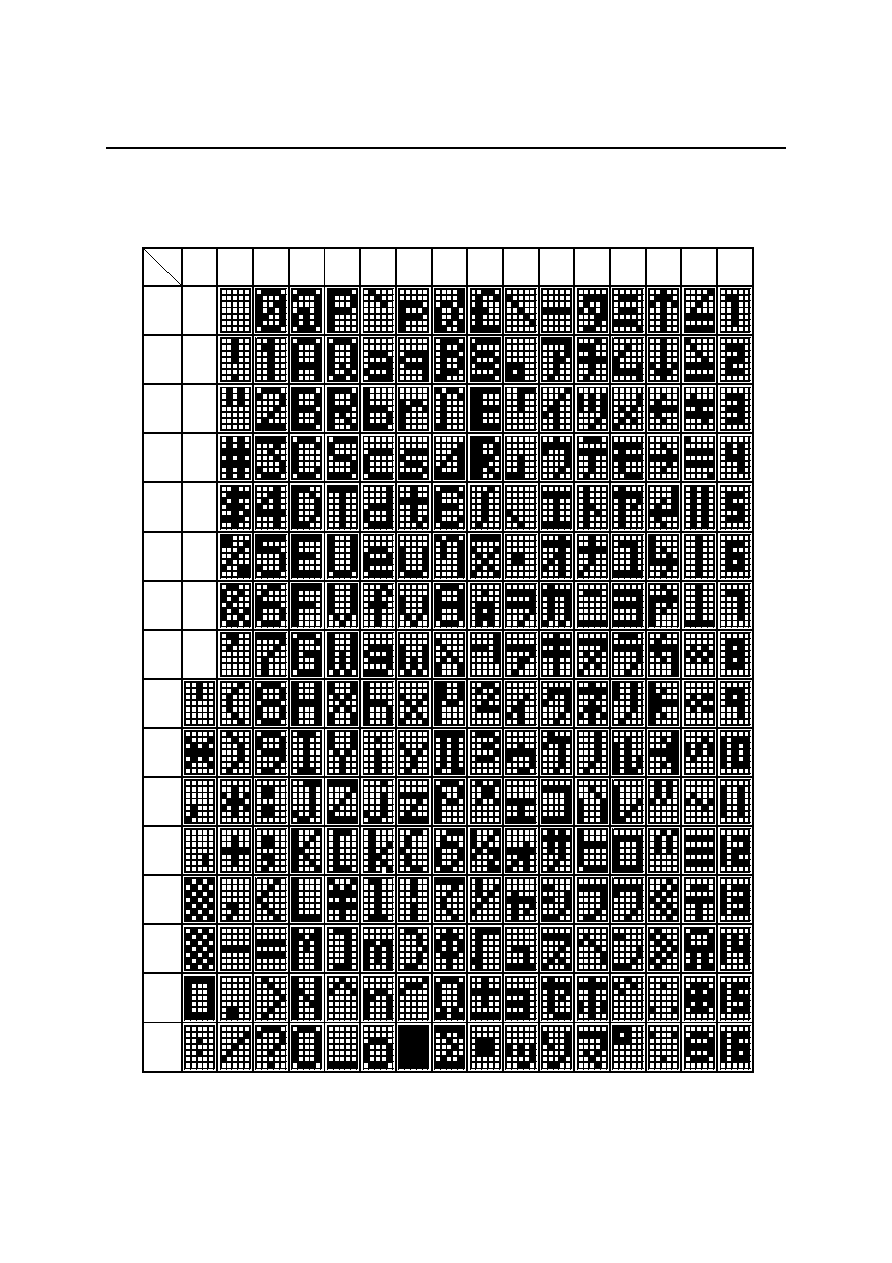
ML9208-01 ROM CODE
* ROM CODE_A is the character set for SEGA1 to SEGA35.
*00000000b(00h) to 00001111b(0Fh) are the CGRAM_A addresses.
MSB
0000 0001 0010 0011 0100 0101 0110 0111 1000 1001 1010 1011 1100 1101 1110 1111
LSB
0000
0001
0010
0011
0100
0101
0110
0111
1000
1001
1010
1011
1100
1101
1110
1111
RAM0
RAM1
RAM2
RAM3
RAM4
RAM5
RAM6
RAM7

FEDL9208-01
OKI Semiconductor
ML9208
30/33
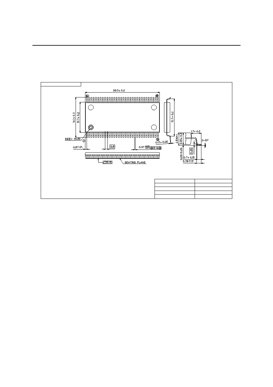
PACKAGE DIMENSIONS
QFP64-P-1414-0.80-BK
Mirror finish
Package material
Epoxy resin
Lead frame material
42 alloy
Pin treatment
Solder plating (
J
5µm)
Package weight (g)
0.87 TYP.
5
Rev. No./Last Revised
6/Feb. 23, 2001
Notes for Mounting the Surface Mount Type Package
The surface mount type packages are very susceptible to heat in reflow mounting and humidity absorbed in storage.
Therefore, before you perform reflow mounting, contact Oki's responsible sales person for the product name,
package name, pin number, package code and desired mounting conditions (reflow method, temperature and
times).
(Unit: mm)
FEDL9208-01
OKI Semiconductor
ML9208
31/33
SSOP64-P-525-0.80-K
Mirror finish
Package material
Epoxy resin
Lead frame material
42 alloy
Pin treatment
Solder plating (
5µm)
Package weight (g)
1.34 TYP.
5
Rev. No./Last Revised
3/Dec. 5, 1996
Notes for Mounting the Surface Mount Type Package
The surface mount type packages are very susceptible to heat in reflow mounting and humidity absorbed in storage.
Therefore, before you perform reflow mounting, contact Oki's responsible sales person for the product name,
package name, pin number, package code and desired mounting conditions (reflow method, temperature and
times).
(Unit: mm)

FEDL9208-01
OKI Semiconductor
ML9208
32/33
REVISION HISTORY
Page
Document
No.
Date
Previous
Edition
Current
Edition
Description
FEDL9208-02
Feb. 23, 2004
≠
≠
Final edition 1

FEDL9208-01
OKI Semiconductor
ML9208
33/33
NOTICE
1. The information contained herein can change without notice owing to product and/or technical improvements.
Before using the product, please make sure that the information being referred to is up-to-date.
2. The outline of action and examples for application circuits described herein have been chosen as an explanation
for the standard action and performance of the product. When planning to use the product, please ensure that the
external conditions are reflected in the actual circuit, assembly, and program designs.
3. When designing your product, please use our product below the specified maximum ratings and within the
specified operating ranges including, but not limited to, operating voltage, power dissipation, and operating
temperature.
4. Oki assumes no responsibility or liability whatsoever for any failure or unusual or unexpected operation
resulting from misuse, neglect, improper installation, repair, alteration or accident, improper handling, or
unusual physical or electrical stress including, but not limited to, exposure to parameters beyond the specified
maximum ratings or operation outside the specified operating range.
5. Neither indemnity against nor license of a third party's industrial and intellectual property right, etc. is granted
by us in connection with the use of the product and/or the information and drawings contained herein. No
responsibility is assumed by us for any infringement of a third party's right which may result from the use
thereof.
6. The products listed in this document are intended for use in general electronics equipment for commercial
applications (e.g., office automation, communication equipment, measurement equipment, consumer
electronics, etc.). These products are not, unless specifically authorized by Oki, authorized for use in any
system or application that requires special or enhanced quality and reliability characteristics nor in any system
or application where the failure of such system or application may result in the loss or damage of property, or
death or injury to humans.
Such applications include, but are not limited to, traffic and automotive equipment, safety devices, aerospace
equipment, nuclear power control, medical equipment, and life-support systems.
7. Certain products in this document may need government approval before they can be exported to particular
countries. The purchaser assumes the responsibility of determining the legality of export of these products and
will take appropriate and necessary steps at their own expense for these.
8. No part of the contents contained herein may be reprinted or reproduced without our prior permission.
Copyright 2004 Oki Electric Industry Co., Ltd.