
1/17
MSM6351/6351L
° Semiconductor
GENERAL DESCRIPTION
The MSM6351/6351L is a low-power microcontroller manufactured in silicon gate CMOS
technology. Integrated into a single chip are ROM, RAM, five I/O ports, serial I/O port, time-
base counter, LCD driver, three interrupts, crystal oscillator, and voltage tripler.
The MSM6351/6351L, which can drive LCD display with higher-count segments, is best suited
to battery powered applications, such as watches and game machines.
The built-in 8-bit or 5-bit serial port provides a data communication capability with external
machines.
FEATURES
∑ Low power consumption
∑ Large capacity memory
∑ ROM
: 4096 words • 15 bits
∑ RAM
: 1024 words • 4 bits
∑ I/O port
Input-output port
: 5 ports • 4 bits (input or output can be specified for each port)
∑ 62 LCD drivers (1/3 duty or 1/4 duty is selectable. Up to 232 segments can be displayed)
∑ Single 1.5 V power supply operation (MSM6351)
Can be changed to 3.0 V specification by mask option (MSM6351L).
∑ Melody function
∑ Built-in watchdog timer
∑ Built-in 8-bit or 5-bit serial port (asynchronous or synchronous selectable)
∑ 32.768 kHz crystal oscillator
∑ Package options:
100-pin plastic QFP (QFP100-P-1420-0.65-K)
(Product name :MSM6351-••GS-K/
MSM6351L-••GS-K)
100-pin plastic QFP (QFP100-P-1420-0.65-L)
(Product name :MSM6351-••GS-L/
MSM6351L-••GS-L)
100-pin plastic QFP (QFP100-P-1420-0.65-BK) (Product name :MSM6351-••GS-BK/
MSM6351L-••GS-BK)
Chip
•• indicates a code number.
° Semiconductor
MSM6351/6351L
Built-in 8 or 5 bit Serial Port and LCD Driver 4-Bit Microcontroller
E2E0010-38-94
This version: Sep. 1998
Previous version: Mar. 1996
2/17
MSM6351/6351L
° Semiconductor
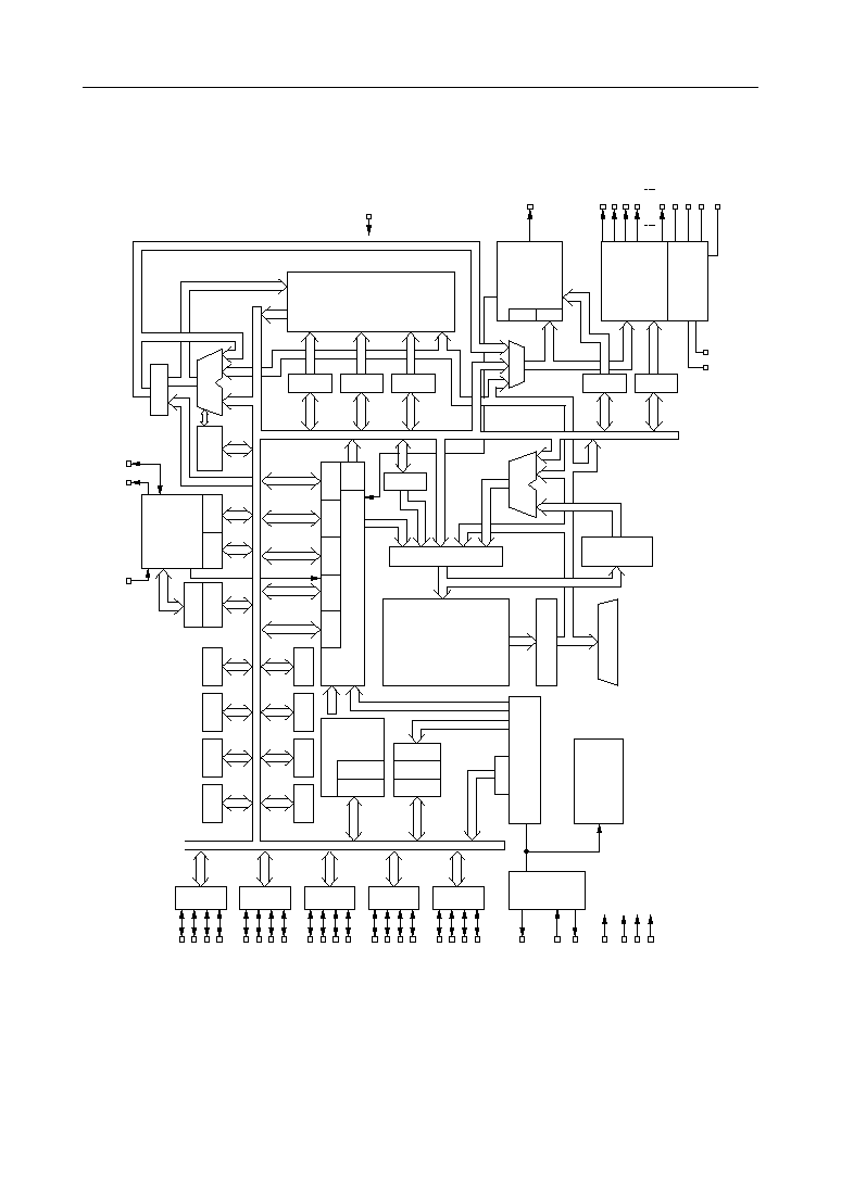
BLOCK DIAGRAM
DATA
RAM
1024•4Bits
BANK
PAGE
WORK
TEMP0
LCD CT
P0.0
P0.1
P0.2
P0.3
P1.0
P1.1
P1.2
P1.3
P2.0
P2.1
P2.2
P2.3
P3.0
P3.1
P3.2
P3.3
P4.0
P4.1
P4.2
P4.3
XTOUT
XT
XT
RESET
TEST1
TEST2
TEST3
SCLK
ACC
ALU
FLAG
SERIAL
I/O
SCNT SCND
SBFF u
SBFF l
D-Bus
P00C
P01C
P02C
P03C
P1•C
P2•C
P3•C
P4•C
IEXM2
IEXM1
IEXM0
IRQRT
EIRT
IRQEX
INTERRUPT CONTROL
FRMT
ADDER
STACK
PROGRAM COUNTER(PC)
INSTRUCTION
DECODER
INSTRUCTION
REGISTER
PROGRAM
ROM
4096•15Bits
P2.0 to P23
WATCH-
DOG
TIMER
WDOG1
WDOG0
TMOUT
TIME BASE COUNTER
SYSTEM
CLOCK
GENERATOR
OSC
PORT4
PORT3
PORT2
PORT1
PORT0
SOUT
SIN
V
DD
V
SS1
V
SS2
VOLTAGE
REGURATOR
CONVERTER
V
CM
V
CP
V
EE
CAPF
CAP0
CAP1
LCD DRIVER
MELODY
MDTH
MDTL
MPX
S-Bus
A-Bus
V
SS3
BD
SEG0
SEG1
SEG2
SEG3
SEG61
3/17
MSM6351/6351L
° Semiconductor
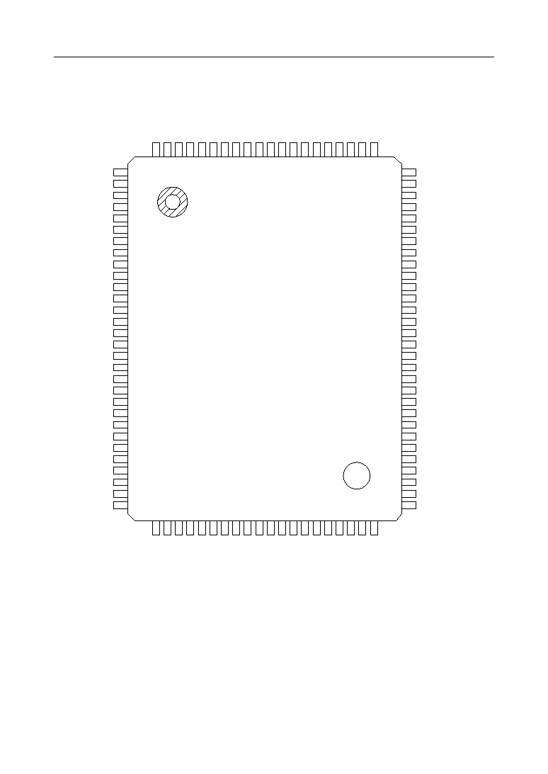
PIN CONFIGURATION (TOP VIEW)
50
1
2
3
4
5
6
7
8
9
10
11
12
13
14
15
16
17
18
19
20
21
22
23
24
25
26
27
28
29
30
SEG0
SEG1
SEG2
SEG3
SEG4
SEG5
SEG6
SEG7
SEG8
SEG9
SEG10
SEG11
SEG12
SEG13
SEG14
SEG15
SEG16
SEG17
SEG18
SEG19
SEG20
SEG21
SEG22
SEG23
SEG24
SEG25
SEG26
SEG27
SEG28
SEG29
49
48
47
46
45
44
43
42
41
40
39
38
37
36
35
34
33
32
31
SEG31
SCLK
SIN
SOUT
V
CM
V
CP
V
EE
V
SS1
V
SS2
V
SS3
V
DD
XT
XT
XTOUT
BD
P1.0
P1.1
P1.2
P1.3
SEG30
80
79
78
77
76
75
74
73
72
71
70
69
68
67
66
65
64
63
62
61
60
59
58
57
56
55
54
53
52
51
SEG61
SEG60
SEG59
SEG58
SEG57
SEG56
SEG55
SEG54
SEG53
SEG52
SEG51
SEG50
SEG49
SEG48
SEG47
SEG46
SEG45
SEG44
SEG43
SEG42
SEG41
SEG40
SEG39
SEG38
SEG37
SEG36
SEG35
SEG34
SEG33
SEG32
P0.0
P0.1
P0.2
P0.3
P2.0
P2.1
P2.2
P2.3
P3.0
P3.1
P3.2
P3.3
P4.0
P4.1
P4.2
P4.3
RESET
TEST1
TEST2
TEST3
81
82
83
84
85
86
87
88
89
90
91
92
93
94
95
96
97
98
99
100
100-Pin Plastic QFP
4/17
MSM6351/6351L
° Semiconductor
PIN DESCRIPTIONS
Symbol
Type
Description
I/O Circuitry
P0.0
∑ 4-bit I/O port 0
P0.1
The input (*) /output, the existence (*) /
absence of pull-down resistance, and the
HALT function release enable/disable (*)
condition can be selected for each bit.
P0.2
P0.3
P1.0 to P1.3
∑ 4-bit I/O port 1
P2.0
I/O
A
P2.1
∑ 4-bit I/O port 2
P2.2
P2.3
P3.0 to P3.3
∑ 4-bit I/O port 3
P4.0 to P4.3
∑ 4-bit I/O port 4
XTOUT
O
∑ Oscillator clock output.
E
XT
O
∑ Oscillator connection pins.
B
XT
I
∑ Reset input.
RESET
I
C
TEST1
TEST2
I
∑ Test input.
D
TEST3
SIN
I
∑ Serial port data input.
F
∑ Serial port data output. When the port is not in an output state,
SOUT
O
G
SCLK
I/O
H
BD
O
∑ Melody output (buzzer drive output).
I
The oscillator clock is output when XTF (bit 3 of port P00C) is set
to "1".
This is an input with a pull-down resistor. The system is reset when
"1" is input.
This is an input with a pull-down resistor.
this pin is set at high-impedance level, except when HZOUT
(bit 3 of port P2XC) =1 and transmitting data.
PORT0
PORT1
PORT2
PORT3
PORT4
Capture
trigger
signal
External
interrupt
signal
The input (*) /output,
the existence (*) /
absence of pull-down
resistance, and the
HALT function
release enable/
disable (*) condition
can be selected for
each port.
∑ Serial port clock input/output.
The input/output (*) is switched by the serial port control register
SCNT. In the output mode, the serial clock frequency can be selected
from the demultiplied signal (1/1, 1/2 or 1/4 of the system clock).
SEG0 to SEG61
O
--
∑ LCD drive output with 1/3 bias and 1/3 duty, or 1/3 bias and 1/4 duty.
The duty can be switched by LCD control register LCDCNT.
A maximum of 177 segments can be displayed when using 1/3 duty
and 232 when using 1/4 duty.
*
Means system reset conditions.
5/17
MSM6351/6351L
° Semiconductor
Output enable
V
SS
V
SS
CMOS inverter
Pull-down enable
V
SS
10 kW
(Standard)
I/O
3-state CMOS buffer
Note:
1.5 V operation∆V
SS1
3.0 V operation∆V
SS2
V
SS
:
Symbol
Description
V
DD
V
SS2
V
SS3
∑ ≠3.0 V power supply pin (for 3.0 V operation)
V
EE
V
CM
∑ Internal voltage converter capacitor connecting pin
∑ ≠1.5 V power supply pin (for 1.5 V operation)
∑ 0 V power supply pin
V
SS1
∑ Internal logic power supply pin
∑ ≠4.5 V power supply pin
V
CP
I/O Circuitry
--
--
--
--
--
--
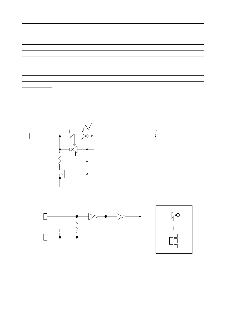
Circuitry on Input/Output Pins
A. Input/output port
B. Oscillator
V
EE
XT
V
EE
V
DD
XT
I
O
a
b
c
a
b
c
V
DD
Note
PIN DESCRIPTIONS (continued)
6/17
MSM6351/6351L
° Semiconductor
Circuitry on Input/Output Pins (continued)
C. RESET input
H. SCLK input/output
D. TEST input
I. BD output
V
DD
Output
resistor
control
V
SS
O
E. XTOUT output
F. SIN input
G. SOUT output
V
SS
O
Output enable
V
SS
CMOS
Schmitt trigger
buffer
V
SS
I
V
SS
I/O
V
SS
Output enable
V
SS
V
SS
I
V
SS
O
V
SS
I

7/17
MSM6351/6351L
° Semiconductor
ABSOLUTE MAXIMUM RATINGS
(MSM6351 (1.5 V Battery), BUF = "0")
Parameter
Symbol
Condition
Rating
Unit
Input Voltage
Output Voltage *1
V
O2
Ta = 25∞C
≠6.0 to +0.3
V
SS1
≠ 0.3 to V
SS1
+ 0.3
V
SS1
≠ 0.3 to V
SS1
+ 0.3
V
Power Supply Voltage
Output Voltage *2
V
IN
V
O1
≠6.0 to +0.3
V
DD
= 0 V (V
SS1
= Battery Voltage)
--
T
STG
Storage Temperature
--
≠55 to +125
∞C
*1 Normal output
*2 LCD driver output
RECOMMENDED OPERATING CONDITIONS
(MSM6351 (1.5 V Battery), BUF = "0")
Parameter
Symbol
Condition
Range
Unit
Operating Voltage
V
op
f
OSC
≠1.75 to ≠1.25
≠20 to +70
32.768
V
∞C
kHz
--
--
BUF = "0"
Operating Frequency
T
op
Operating Temperature
V
DD
= 0 V (V
SS1
= Battery Voltage)

8/17
MSM6351/6351L
° Semiconductor
ELECTRICAL CHARACTERISTICS
(MSM6351 (1.5 V Battery), BUF = "0")
PORT0 to
PORT4 *3,
SOUT, SCLK,
XTOUT
Parameter
Symbol
Condition
Applied Pin
V
DD
= 0 V, V
SS1
= ≠1.5 V (Battery Voltage), V
SS2
= ≠3.0 V, V
SS3
= ≠4.5 V, f
OSC
= 32.768 kHz, C
X
= 35 pF, Ta = 25∞C
Min. Typ. Max. Unit
Power Supply Current
Voltage for Oscillation Start
Output Current 1
Input Current 1
Input Leakage Current
Input Current 3
Input Voltage
I
DD
≠V
OSC
≠I
OH1
I
OMH1
I
OML1
≠I
OL1
≠I
IH1
≠I
IH3
≠V
IH
≠V
IL
*1 *2
Within 2 sec.
V
OH
= ≠0.2 V
V
OMH
= V
SS1
±0.2 V
V
OML
= V
SS2
±0.2 V
V
OL
= ≠4.3 V
V
I
= 0 V
I/O input
With pull-down resistor
V
I
= 0 V
With pull-down resistor
3.0
--
--
1.4
4
--
--
4
--
--
4
--
--
4
--
--
75
150
300
--
--
1
--
4
--
--
--
0.3
1.2
--
--
mA
V
mA
mA
mA
mA
V
PORT0
to
PORT4
RESET
All input pins
V
I
= 0 V, ≠1.5 V
I/O input
Without pull-down resistor
PORT0 to
PORT4,
SCLK, SIN,
SOUT
--
--
--
--
--
--
I
IL2
Output Current 2
Output Current 3
≠I
OH2
mA
mA
I
OL2
≠I
OH3
I
OL3
V
O
= ≠0.5 V
V
O
= ≠1.0 V
V
O
= ≠0.5 V
V
O
= ≠1.0 V
Common/Segment
Output
150
--
--
150
--
--
7
--
--
20
--
--
SEG0
to
SEG61
BD
*1 This value depends on program.
*2 BUF = "0"
*3 PORT0 = P0.0 to P0.3, PORT1 = P1.0 to P1.3, PORT2 = P2.0 to P2.3, PORT3 = P3.0 to P3.3,
PORT4 = P4.0 to P4.3
9/17
MSM6351/6351L
° Semiconductor
ABSOLUTE MAXIMUM RATINGS
(MSM6351L (3.0 V Battery), Halver used (BUF = "0"))
Parameter
Symbol
Condition
Rating
Unit
Input Voltage
Output Voltage *1
V
O2
Ta = 25∞C
≠6.0 to +0.3
V
SS2
≠ 0.3 to V
SS2
+ 0.3
V
SS2
≠ 0.3 to V
SS2
+ 0.3
V
Power Supply Voltage
Output Voltage *2
V
IN
V
O1
≠6.0 to +0.3
V
DD
= 0 V (V
SS2
= Battery Voltage)
--
T
STG
Storage Temperature
--
≠55 to +125
∞C
*1 Normal output
*2 LCD driver output
RECOMMENDED OPERATING CONDITIONS
(MSM6351L (3.0 V Battery), Halver used (BUF = "0"))
Parameter
Symbol
Condition
Range
Unit
Operating Voltage
V
op
f
OSC
≠3.5 to ≠2.6
≠20 to +70
32.768
V
∞C
kHz
--
--
Halver used (BUF = "0")
Operating Frequency
T
op
Operating Temperature
V
DD
= 0 V (V
SS2
= Battery Voltage)

10/17
MSM6351/6351L
° Semiconductor
ELECTRICAL CHARACTERISTICS
(MSM6351L (3.0 V Battery), Halver used (BUF="0"))
PORT0 to
PORT4 *3,
SOUT, SCLK,
XTOUT
Parameter
Symbol
Condition
Applied Pin
V
DD
= 0 V, V
SS1
= ≠1.5 V, V
SS2
= ≠3.0 V (Battery Voltage), V
SS3
= ≠4.5 V, f
OSC
= 32.768 kHz, C
X
= 35 pF, Ta = 25∞C
Min. Typ. Max. Unit
Power Supply Current
Voltage for Oscillation Start
Output Current 1
Input Current 1
Input Leakage Current
Input Current 3
Input Voltage
I
DD
≠V
OSC
≠I
OH1
I
OMH1
I
OML1
≠I
OL1
≠I
IH1
≠I
IH3
≠V
IH
≠V
IL
*1 *2
Within 2 sec.
V
OH
= ≠0.2 V
V
OMH
= V
SS1
±0.2 V
V
OML
= V
SS2
±0.2 V
V
OL
= ≠4.3 V
V
I
= 0 V
I/O input
With pull-down resistor
V
I
= 0 V
With pull-down resistor
1.5
--
--
2.4
4
--
--
4
--
--
4
--
--
4
--
--
150
300
600
--
--
1
--
25
--
--
--
0.5
2.5
--
--
mA
V
mA
mA
mA
mA
V
PORT0
to
PORT4
RESET
All input pins
V
I
= 0 V, ≠3 V
I/O input
Without pull-down resistor
PORT0 to
PORT4,
SCLK, SIN,
SOUT
--
--
--
--
--
--
I
IL2
Output Current 2
Output Current 3
≠I
OH2
mA
mA
≠I
OL2
≠I
OH3
≠I
OL3
V
O
= ≠0.5 V
V
O
= ≠2.5 V
V
O
= ≠0.5 V
V
O
= ≠2.5 V
Common/Segment
Output
500
--
--
500
--
--
7
--
--
20
--
--
SEG0
to
SEG61
BD
*1 This value depends on program.
*2 When 3 V battery with halver is used (BUF = "0")
*3 PORT0 = P0.0 to P0.3, PORT1 = P1.0 to P1.3, PORT2 = P2.0 to P2.3, PORT3 = P3.0 to P3.3,
PORT4 = P4.0 to P4.3

11/17
MSM6351/6351L
° Semiconductor
ABSOLUTE MAXIMUM RATINGS
(MSM6351L (3.0 V Battery), Halver not used (BUF = "1"))
Parameter
Symbol
Condition
Rating
Unit
Input Voltage
Output Voltage *1
V
O2
Ta = 25∞C
≠6.0 to +0.3
V
SS2
≠ 0.3 to +0.3
V
SS2
≠ 0.3 to +0.3
V
Power Supply Voltage
Output Voltage *2
V
IN
V
O1
≠6.0 to +0.3
V
DD
= 0 V (V
SS2
= Battery Voltage)
--
T
STG
Storage Temperature
--
≠55 to +125
∞C
*1 Normal output
*2 LCD driver output
RECOMMENDED OPERATING CONDITIONS
(MSM6351L (3.0 V Battery), Halver not used (BUF = "1"))
Parameter
Symbol
Condition
Range
Unit
Operating Voltage
V
op
f
OSC
≠3.5 to ≠2.2
≠20 to +70
32.768
V
∞C
kHz
--
--
Halver not used (BUF = "1")
Operating Frequency
T
op
Operating Temperature
V
DD
= 0 V (V
SS2
= Battery Voltage)

12/17
MSM6351/6351L
° Semiconductor
ELECTRICAL CHARACTERISTICS
(MSM6351L (3.0 V Battery), Halver not used (BUF="1"))
*1 This value depends on program.
*2 When halver is not used (BUF = "1")
*3 PORT0 = P0.0 to P0.3, PORT1 = P1.0 to P1.3, PORT2 = P2.0 to P2.3, PORT3 = P3.0 to P3.3,
PORT4 = P4.0 to P4.3
PORT0 to
PORT4 *3,
SOUT, SCLK,
XTOUT
Parameter
Symbol
Condition
Applied Pin
V
DD
= 0 V, V
SS1
= ≠1.5 V, V
SS2
= ≠3.0 V (Battery Voltage), V
SS3
= ≠4.5 V, f
OSC
= 32.768 kHz, C
X
= 35 pF, Ta = 25∞C
Min. Typ. Max. Unit
Power Supply Current
Voltage for Oscillation Start
Output Current 1
Input Current 1
Input Leakage Current
Input Current 3
Input Voltage
I
DD
≠V
OSC
≠I
OH1
I
OMH1
I
OML1
≠I
OL1
≠I
IH1
≠I
IH3
≠V
IH
≠V
IL
*1 *2
Within 2 sec.
V
OH
= ≠0.2 V
V
OMH
= V
SS1
±0.2 V
V
OML
= V
SS2
±0.2 V
V
OL
= ≠4.3 V
V
I
= 0 V
I/O input
With pull-down resistor
V
I
= 0 V
With pull-down resistor
3.0
--
--
2.4
4
--
--
4
--
--
4
--
--
4
--
--
150
300
600
--
--
1
--
25
--
--
--
0.5
2.5
--
--
mA
V
mA
mA
mA
mA
V
PORT0
to
PORT4
RESET
All input pins
V
I
= 0 V, ≠3 V
I/O input
Without pull-down resistor
PORT0 to
PORT4,
SCLK, SIN,
SOUT
--
--
--
--
--
--
I
IL2
Output Current 2
Output Current 3
≠I
OH2
mA
mA
≠I
OL2
≠I
OH3
≠I
OL3
V
O
= ≠0.5 V
V
O
= ≠2.5 V
V
O
= ≠0.5 V
V
O
= ≠2.5 V
Common/Segment
Output
500
--
--
500
--
--
7
--
--
20
--
--
SEG0
to
SEG61
BD
13/17
MSM6351/6351L
° Semiconductor
INSTRUCTION LIST
i
3
i
2
i
1
i
0
i
3
i
2
i
1
i
0
i
3
i
2
i
1
i
0
Mnemonic
Instruction code
Description
14
0
ADD ACC, REG1
(rP), (ACC), (Z), (C)®(rP) + (ACC)
0
ADD #i, REG1
(rP), (ACC), (Z), (C)®(rP) +i
0
ADC REG1
(rP), (ACC), (Z), (C)®decimal adj [(rP) + (ACC) + (C)]
0
ADCN REG1
(rP), (ACC), (Z), (C)®N adjust [(rP) + (C)]
0
SUB ACC, REG1
(rP), (ACC), (Z), (C)®(rP) + (ACC)
0
SUB #i, REG1
(rP), (ACC), (Z), (C)®(rP) ≠i
0
SBC REG1
(rP), (ACC), (Z), (C)®decimal adj [(rP) ≠ (ACC) ≠ (C)]
0
SBCN REG1
(rP), (ACC), (Z), (C)®N adjust [(rP) ≠ (C)]
0
CMP ACC, REG1
(Z), (C)®(rP) ≠ (ACC)
0
CMP #i, REG1
(Z), (C)®(rP) ≠ i
0
INC REG1
(rP), (ACC), (Z), (C)®(rP) +1
1
INCD REG2
(rPb), (ACC), (Z), (C)®(rPb) +1
0
DEC REG1
(rP), (ACC), (Z), (C)®(rP) ≠1
1
DECD REG2
(rPb), (ACC), (Z), (C)®(rPb) ≠1
0
BIT ACC, REG1
(Z)®(rP
3
) (ACC3) (rP
2
) (ACC2) (rP
1
) (ACC1)
(rP
0
) (ACC0)
0
BIT #i, REG1
(Z)®(rP
3
) i
3
(rP
2
) i
2
(rP
1
) i
1
(rP
0
) i
0
0
BIS ACC, REG1
(rP), (ACC), (Z)®(rP) (ACC)
0
BIS #i, REG1
(rP), (ACC), (Z)®(rP) i
0
BIC ACC, REG1
(rP), (ACC), (Z)®(rP) (ACC)
0
BIC #1, REG1
(rP), (ACC), (Z)®(rP) i
0
XOR ACC, REG1
(rP), (ACC), (Z)®(rP) (ACC)
0
XOR #1, REG1
(rP), (ACC), (Z)®(rP) i
0
ROR REG1
(Z), (ACC)®[ ∆(C)∆(rP)∆ ]
0
ROL REG1
(Z), (ACC)®[ ®(C)®(rP)® ]
0
ASR REG1
(Z), (ACC)®[O∆(rP)∆(C)]
0
ASL REG1
(Z), (ACC)®[(C)®(rP)®O]
0
CLG
(G)®O
0
CLC
(C)®O
0
CLZ
(Z)®O
0
CLA
(Z), (C), (G)®O
13
0
0
0
1
0
0
0
1
0
0
0
0
0
0
0
0
0
0
0
0
0
0
0
0
0
0
0
0
0
0
12
0
1
0
1
0
1
0
1
0
1
0
0
0
0
0
1
0
1
0
1
0
1
0
0
0
0
0
0
0
0
11
0
1
0
0
0
1
0
0
0
0
0
0
0
1
0
0
0
0
0
0
0
1
0
0
0
0
0
0
0
0
10
0
0
0
0
0
0
0
0
0
1
0
b
1
0
b
1
0
1
0
0
0
0
0
1
0
0
0
0
0
0
0
0
9
0
0
0
0
1
1
1
1
1
1
0
b
0
1
b
0
0
0
0
0
1
1
0
1
0
1
0
1
0
0
0
0
8
P
P
P
P
P
P
P
P
P
P
P
0
P
0
P
P
P
P
P
P
P
P
P
P
P
P
0
0
0
0
7
0
i
3
0
N
3
0
0
N
3
1
i
3
0
P
3
0
P
3
1
i
3
0
i
3
0
0
0
0
0
0
1
1
1
1
6
1
i
2
1
N
2
1
1
N
2
1
i
2
0
P
2
0
P
2
1
i
2
1
i
2
1
1
0
0
0
0
0
0
0
0
5
0
i
1
0
N
1
0
0
N
1
1
i
1
0
P
1
0
P
1
1
i
1
1
i
1
1
1
1
1
1
1
0
0
1
1
4
0
i
0
1
N
0
0
1
N
0
0
i
0
1
P
0
1
P
0
0
i
0
0
i
0
0
1
0
0
1
1
0
1
0
1
3
r
3
2
r
2
1
r
1
0
r
0
Ma-
chine
cycle
r
3
r
2
r
1
r
0
r
3
r
2
r
1
r
0
r
3
r
2
r
1
r
0
r
3
r
2
r
1
r
0
r
3
r
2
r
1
r
0
r
3
r
2
r
1
r
0
r
3
r
2
r
1
r
0
r
3
r
2
r
1
r
0
r
3
r
2
r
1
r
0
r
3
r
2
r
1
r
0
r
3
r
2
r
1
r
0
r
3
r
2
r
1
r
0
r
3
r
2
r
1
r
0
r
3
r
2
r
1
r
0
r
3
r
2
r
1
r
0
r
3
r
2
r
1
r
0
r
3
r
2
r
1
r
0
r
3
r
2
r
1
r
0
r
3
r
2
r
1
r
0
r
3
r
2
r
1
r
0
r
3
r
2
r
1
r
0
r
3
r
2
r
1
r
0
r
3
r
2
r
1
r
0
r
3
r
2
r
1
r
0
r
3
r
2
r
1
r
0
0 0 0 0
0 0 0 0
0 0 0 0
0 0 0 0
1
1
1
1
1
1
1
1
1
1
1
1
1
1
1
1
1
1
1
1
1
1
1
1
1
1
1
1
1
1
0
SEG
(G)®1
0 0 0 0 1 0 1 0 0 0 0 0 0 0
1
0
SEC
(C)®1
0 0 0 0 1 0 1 0 0 1 0 0 0 0
1
0
SEZ
(Z)®1
0 0 0 0 1 0 1 0 1 0 0 0 0 0
1
0
SEA
(Z), (C), (G)®1
0 0 0 0 1 0 1 0 1 1 0 0 0 0
1
Arithmetic operation instruction
Bit manipulation instruction
Rotate instruction
Flag operation instruction
14/17
MSM6351/6351L
° Semiconductor
INSTRUCTION LIST (continued)
0 0 0 0
Mnemonic
Instruction code
Description
14
0
MOV ACC, REG1
(rP)®(ACC)
1
MOVD ACC, REG2
(rPb)®(ACC)
0
MOV #i, REG1
(rP), (ACC), (Z)®i
0
MOV REG1, ACC
(ACC), (Z)®(rP)
1
MOVD REG2, ACC
(ACC), (Z)®(rPb)
0
EXG REG1
(rP)¥(ACC)
0
EXGD REG2
(rPb)¥(ACC)
1
CALL adrs
(STACK)®(PC), (PC)®a
11
to a
0
, (SP)®(SP)+1
0
RET
(PC)®(STACK)+1, (SP)®(SP)≠1
0
RTI
(PC)®(STACK)+1, (SP)®(SP)≠1 (at INT routine)
13
0
0
0
0
0
0
1
1
0
0
12
0
1
1
0
1
0
1
1
0
0
11
0
0
1
0
1
0
1
a
11
0
0
10
0
b
1
1
0
b
1
0
b
1
a
10
0
0
9
0
b
0
0
1
b
0
1
b
0
a
9
0
1
8
P
0
P
P
0
P
0
a
8
0
0
7
1
P
3
i
3
1
P
3
P
3
a
7
1
1
6
1
P
2
i
2
1
P
2
P
2
a
6
1
1
5
1
P
1
i
1
1
P
1
P
1
a
5
0
0
4
1
P
0
i
0
1
P
0
P
0
a
4
0
0
3
r
3
2
r
2
1
r
1
0
r
0
Ma-
chine
cycle
r
3
r
2
r
1
r
0
r
3
r
2
r
1
r
0
r
3
r
2
r
1
r
0
r
3
r
2
r
1
r
0
r
3
r
2
r
1
r
0
r
3
r
2
r
1
r
0
a
3
a
2
a
1
a
0
0 0 0 0
0 0 0 0
1
1
1
1
1
1
1
1
1
1
Data transfer instruction
Subroutine instruciton
0
BGT n
if (G)=1
then (PC)®(PC)+N else (PC)®(PC)+1
0 0 0 1 1 P 0 0 1 n
4
n
3
n
2
n
1
n
0
1
0
BLE n
if (G)=0
then (PC)®(PC)+N else (PC)®(PC)+1
0 0 0 1 1 P 1 0 1 n
4
n
3
n
2
n
1
n
0
1
0
BCS n
if (C)=1
then (PC)®(PC)+N else (PC)®(PC)+1
0 0 0 1 1 P 0 0 0 n
4
n
3
n
2
n
1
n
0
1
0
BCC n
if (C)=0
then (PC)®(PC)+N else (PC)®(PC)+1
0 0 0 1 1 P 1 0 0 n
4
n
3
n
2
n
1
n
0
1
0
BEQ n (BZE n)
if (Z)=1
then (PC)®(PC)+N else (PC)®(PC)+1
0 0 0 1 1 P 0 1 0 n
4
n
3
n
2
n
1
n
0
1
0
BNE n (BNZ n)
if (Z)=0
then (PC)®(PC)+N else (PC)®(PC)+1
0 0 0 1 1 P 1 1 0 n
4
n
3
n
2
n
1
n
0
1
0
BGE n
if {(G)=1 or (Z)=1}
then (PC)®(PC)+N else (PC)®(PC)+1
0 0 0 1 1 P 0 1 1 n
4
n
3
n
2
n
1
n
0
1
0
BLT n
if {(G)=0 and (Z)=0}
then (PC)®(PC)+N else (PC)®(PC)+1
0 0 0 1 1 P 1 1 1 n
4
n
3
n
2
n
1
n
0
1
0
MSA adrs *
Specifies the first address of note data. (E00
H
~FFF
H
)
0 0 0 1 0 a
8
a
7
a
6
a
5
a
4
a
3
a
2
a
1
a
0
2
0
DSP dig, REG1 *
digit (Low Part)®(rP), (ACC)
0 0 1 0 0 P dig
3
dig
2
dig
1
dig
0
r
3
r
2
r
1
r
0
1
0
DSPH dig, REG1 *
digit (High Part)®(rP), (ACC)
0 0 1 0 1 P dig
3
dig
2
dig
1
dig
0
r
3
r
2
r
1
r
0
1
0
DSPF dig, REG1 *
digit (Low Part)®(rP) via Table
0 0 1 1 0 P dig
3
dig
2
dig
1
dig
0
r
3
r
2
r
1
r
0
2
0
DSPF dig, REG1 *
digit (Low Part)®(rP) via Table
0 0 1 1 1 P dig
3
dig
2
dig
1
dig
0
r
3
r
2
r
1
r
0
2
0
OUT REG1, PORT
(PORTy)®(rP)
1 0 1 0 y
4
P y
3
y
2
y
1
y
0
r
3
r
2
r
1
r
0
1
0
OUT #i, PORT
(PORTy)®i
1 0 1 1 y
4
P y
3
y
2
y
1
y
0
i
3
i
2
i
1
i
0
1
0
INP PORT, REG1
(rP), (ACC)®(PORTy)
1 0 0 0 y
4
P y
3
y
2
y
1
y
0
r
3
r
2
r
1
r
0
1
0
NOP
NO Operation
0 0 0 0 0 0 0 0 0 0 0 0 0 0
1
0
HALT
HAIT CPU
0 0 0 0 1 0 0 1 1 1 0 0 0 0
1
Jump instruction
Melody
start
Display
instruction
Input/output instruction
CPU
control
When P=0
in bit 8,
N=n+1;
when P=1,
N=≠n.
1
JMP adrs
(PC)®a
11
to a
0
0
AMP @ REG1
(PC)®(PC)+(rP)+1
0
JMPO @ REG1
(PC)®(PC)+7 (rP)+1
1
0
0
0
0
0
a
11
0
0
a
10
0
0
a
9
0
1
a
8
0
0
a
7
1
1
a
6
1
1
a
5
0
0
a
4
1
1
a
3
a
2
a
1
a
0
r
3
r
2
r
1
r
0
1
1
1
r
3
r
2
r
1
r
0

15/17
MSM6351/6351L
° Semiconductor
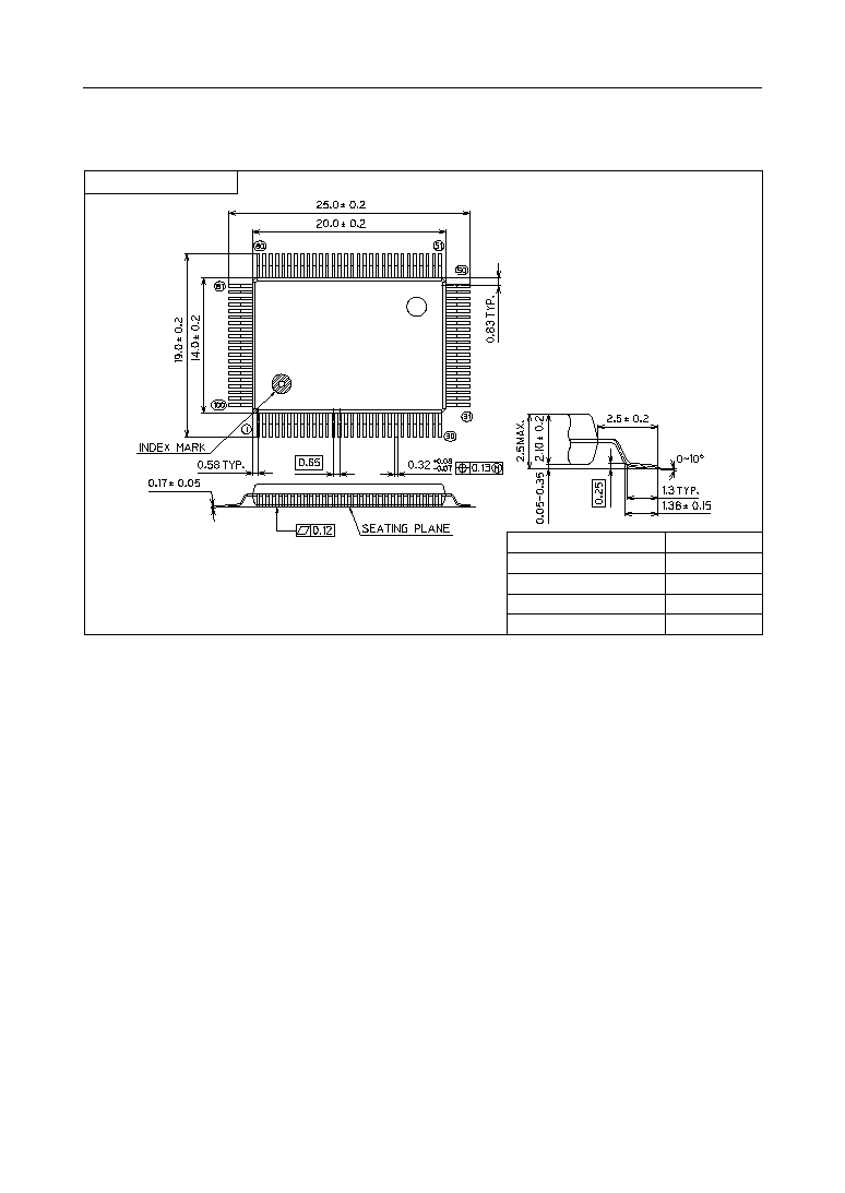
(Unit : mm)
PACKAGE DIMENSIONS
Notes for Mounting the Surface Mount Type Package
The SOP, QFP, TSOP, SOJ, QFJ (PLCC), SHP and BGA are surface mount type packages, which
are very susceptible to heat in reflow mounting and humidity absorbed in storage.
Therefore, before you perform reflow mounting, contact Oki's responsible sales person for the
product name, package name, pin number, package code and desired mounting conditions
(reflow method, temperature and times).
QFP100-P-1420-0.65-K
Package material
Lead frame material
Pin treatment
Solder plate thickness
Package weight (g)
Epoxy resin
42 alloy
Solder plating
5 mm or more
1.29 TYP.
Mirror finish

16/17
MSM6351/6351L
° Semiconductor
(Unit : mm)
Notes for Mounting the Surface Mount Type Package
The SOP, QFP, TSOP, SOJ, QFJ (PLCC), SHP and BGA are surface mount type packages, which
are very susceptible to heat in reflow mounting and humidity absorbed in storage.
Therefore, before you perform reflow mounting, contact Oki's responsible sales person for the
product name, package name, pin number, package code and desired mounting conditions
(reflow method, temperature and times).
QFP100-P-1420-0.65-L
Package material
Lead frame material
Pin treatment
Solder plate thickness
Package weight (g)
Epoxy resin
42 alloy
Solder plating
5 mm or more
1.29 TYP.
Spherical surface
17/17
MSM6351/6351L
° Semiconductor
(Unit : mm)
Notes for Mounting the Surface Mount Type Package
The SOP, QFP, TSOP, SOJ, QFJ (PLCC), SHP and BGA are surface mount type packages, which
are very susceptible to heat in reflow mounting and humidity absorbed in storage.
Therefore, before you perform reflow mounting, contact Oki's responsible sales person for the
product name, package name, pin number, package code and desired mounting conditions
(reflow method, temperature and times).
QFP100-P-1420-0.65-BK
Package material
Lead frame material
Pin treatment
Solder plate thickness
Package weight (g)
Epoxy resin
42 alloy
Solder plating
5 mm or more
1.29 TYP.
Mirror finish