 | –≠–ª–µ–∫—Ç—Ä–æ–Ω–Ω—ã–π –∫–æ–º–ø–æ–Ω–µ–Ω—Ç: MSM6389C | –°–∫–∞—á–∞—Ç—å:  PDF PDF  ZIP ZIP |

° Semiconductor
MSM6389C
1/11
GENERAL DESCRIPTION
The MSM6389C is a solid-state recorder data register in 1,048,576 words x 1 bit configuration.
The MSM6389C has a built-in internal address generator circuit allowing continuous serial read/
write operation by single external clock input. The internal address is automatically incremented by
one by read/write operation.
Address designation in units of 1024 words in the direction of words is possible by an external serial
address input.
The built-in refresh timer and refresh counter have eliminated the need of an external refresh circuit
and realized a low power consumption.
18-pin plastic QFJ is used as the package and the operating temperature range is between 0
∞
C and
70
∞
C.
The MSM6389C is suitable for storing large capacity data with battery backup. A solid state recording
and playback system can easily be constructed in combination with OKI's voice synthesizer ICs.
FEATURES
∑ Configuration:
1,048,576 x 1 bit
∑ Serial access operation:
Serial access time
1.5 ms (3.0 ms)
Serial read/write cycle time
2.0 ms (4.0 ms)
Fast mode read/write cycle time 0.4 ms (0.4 ms)
Times in parentheses indicate ones in self-refresh mode.
∑ Low current consumption:
100 mA max. (for data holding, V
CC
=4.0V)
∑ Wide operating supply voltage range:
Single 3.5 to 5.5V
∑ Auto-refresh/self-refresh changeable
∑ Package:
18-pin plastic QFJ (QFJ18-P-R290-1.27) (Product name: MSM6389CJS)
° Semiconductor
MSM6389C
1,048,576-Word x 1-Bit Solid-State Recorder Data Register
E2D0033-39-21
This version: Feb. 1999
Previous version: May. 1997

° Semiconductor
MSM6389C
2/11
BLOCK DIAGRAM
Sin
Address
Register
X-address
Counter
Pout
Clock
Load
Clock
Refresh
Counter
Clock
Timing
Generator
Refresh
Timer
Address
Multiplexer
X-decoder/
Driver
Y-decoder/sense Amp
Y-address Counter
Reset
Clock
1,048,576
Data Register
Write
Clock
Generator
I/O
Controller
V
BB
Generator
SAD
CS
SAS
FAM
RWCK
TEST
RFSH
RS/A
TAS
WE
DOUT
DIN
V
SS
V
CC
TEST
PIN CONFIGURATION (TOP VIEW)
3
2
8
16
WE DIN V
SS
DOUT
TEST
CS
NC
SAD
SAS
TEST
NC
NC
RWCK
FAM
TAS V
CC
RS/A
RFSH
4
15
5
14
6
13
7
12
1
9
18
10
17
11
NC: No connection
18-Pin Plastic QFJ

° Semiconductor
MSM6389C
3/11
PIN DESCRIPTIONS
Data input
Pin
Description
1
Write enable
2
Test input
3, 16
Chip select
4
Serial address data
6
Serial address strobe
7
Transfer address strobe
8
Power supply (+5V)
9
Self-refresh/auto-refresh select
10
Refresh clock input
11
Fast access mode select
12
Read/write clock
13
Data output
17
Ground (0V)
18
Symbol
DIN
WE
TEST
CS
SAD
SAS
TAS
V
CC
RS/A
RFSH
FAM
RWCK
DOUT
V
SS
° Semiconductor
MSM6389C
4/11
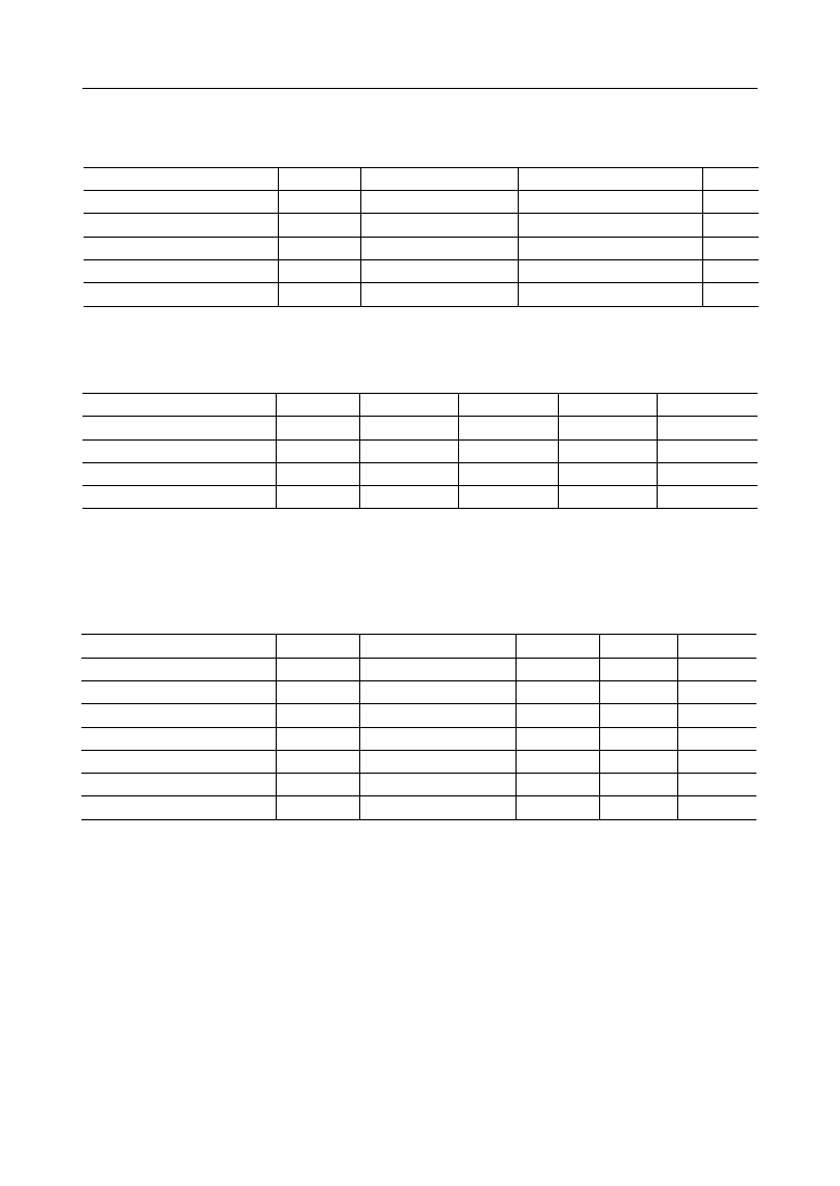
ABSOLUTE MAXIMUM RATINGS
Parameter
Symbol
Condition
Rating
Unit
Terminal Voltage
V
T
Ta = 25∞C, relative to V
SS
≠1.0 to +7.0
V
Output Short-Circuit Current
I
OS
Ta = 25∞C
50
mA
Power Dissipation
P
D
Ta = 25∞C
1
W
Operating Temperature
T
op
--
0 to 70
∞C
Storage Temperature
T
STG
--
≠55 to +150
∞C
RECOMMENDED OPERATING CONDITIONS
Parameter
Symbol
Min.
Typ.
Max.
Unit
Supply Voltage
V
CC
3.5
4.5
5.5
V
Supply Voltage
V
SS
0
0
0
V
V
IH
V
CC
≠ 0.5
V
CC
V
CC
+ 0.5
V
V
IL
≠0.5
0
+0.5
V
"H" Input Voltage
"L" Input Voltage
(Ta = 0 to 70∞C)
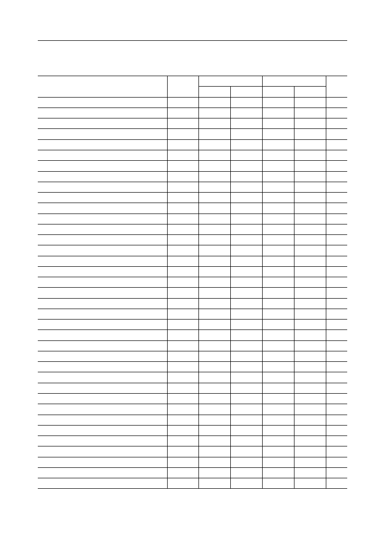
ELECTRICAL CHARACTERISTICS
DC Characteristics
Parameter
Symbol
Condition
Min.
Max.
Unit
"H" Output Voltage
V
OH
I
OH
= ≠0.5 mA
V
CC
≠ 0.5
--
V
"L" Output Voltage
V
OL
I
OL
= 0.5 mA
--
0.4
V
Input Leakage Current
I
LI
V
I
= 0 V to V
CC
≠1
+1
mA
Output Leakage Current
I
LO
V
O
= 0 V to V
CC
≠1
+1
mA
Supply Current (in operating state)
I
CC1
V
CC
= 4 V, t
RWC
= 2 µs
--
5
mA
Supply Current (FAM)
I
CC3
V
CC
= 4 V, t
RWC
= 0.4 ms
--
15
mA
Supply Current (in standby state)
I
CC2
V
CC
= 4 V
--
100
mA
(V
CC
= 3.5 V to 5.5 V, Ta = 0 to 70∞C)
° Semiconductor
MSM6389C
5/11
AC Characteristics
Note: Switching to the fast mode should be made satisfying the timings of t
FS
and t
SS
at the "L" level
of RWCK.
Parameter
Symbol
Min.
Max.
Min.
Max.
Unit
MSM6389C-SELF
MSM6389C-AUTO
--
--
--
100
Refresh Cycle
t
REF
ms
4,000
--
2,000
--
Read/Write Cycle Time
t
RWC
ns
--
3,000
--
1,500
Access Time
t
ACC
ns
0
50
0
50
Output Turn-off Delay Time
t
OFF
ns
3
50
3
50
Input Signal Rise/Fall Time
t
T
ns
1,000
--
500
--
RWCK Precharge Time
t
RWP
ns
3,000
10,000
1,500
10,000
RWCK Pulse Width
t
RW
ns
100
--
100
--
SAS Cycle Time
t
SSC
ns
50
--
50
--
SAS Pulse Width
t
SAS
ns
50
--
50
--
SAS Precharge Time
t
SAP
ns
0
--
0
--
Address Setup Time
t
AS
ns
50
--
50
--
Address Hold Time
t
AH
ns
50
--
50
--
TAS Setup Time
t
ATS
ns
50
--
50
--
TAS to RWCK Setup Time
t
TRS
ns
50
--
50
--
TAS Pulse Width
t
TAS
ns
0
--
0
--
Read Command Setup Time
t
RRS
ns
50
--
50
--
Read Command Hold Time
t
RRH
ns
0
--
0
--
Write Command Setup Time
t
WRS
ns
50
--
50
--
Write Command Hold Time
t
WRH
ns
50
--
50
--
Write Command Pulse Width
t
WP
ns
50
--
50
--
WE to RWCK Lead Tme
t
RWL
ns
0
--
0
--
Data Setup Time
t
DS
ns
50
--
50
--
Data Hold Time
t
DH
ns
100
--
100
--
RWCK to WE Delay Time
t
RWD
ns
--
--
500
--
RFSH Setup Time
t
RFS
ns
--
--
500
--
RFSH Precharge Time
t
RFP
ns
--
--
1,500
10,000
RFSH Pulse Width
t
RF
ns
--
--
500
--
RFSH RWCK Precharge Time
t
RRP
ns
400
--
400
--
Fast Mode Cycle Time
t
FC
ns
--
300
--
300
Fast RWCK Mode Access Time
t
FAC
ns
100
--
100
--
Fast RWCK Precharge Time
t
FCP
ns
300
--
300
--
Fast Mode RWCK Pulse Width
t
FR
ns
0
--
0
--
Fast Mode Setup Time
t
FS
ns
50
--
50
--
Fast Mode Hold Time
t
FH
ns
4,000
100,000
2,000
100,000
Fast Mode Width
t
FCC
ns
0
--
0
--
Slow Mode Setup Time
t
SS
ns
50
--
50
--
Slow Mode Hold Time
t
SH
ns
(V
CC
= 3.5 V to 5.5 V, Ta = 0 to 70∞C)

° Semiconductor
MSM6389C
6/11
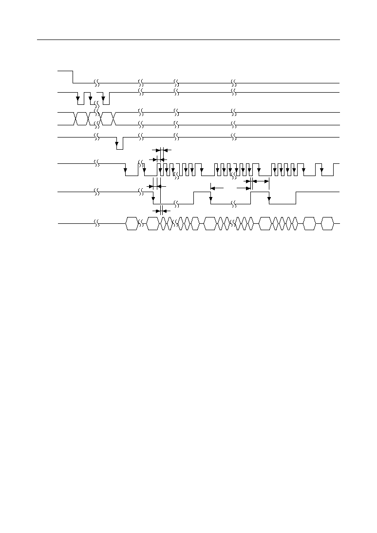
TIMING DIAGRAMS
Read/Write/Read Modify Write Cycle
CS
t
RW
t
RWF
t
RW
t
RWC
t
SAS
t
SSC
t
SAP
t
TRS
t
AS
t
AH
A0
A1
A2
A9
t
TAS
t
ATS
t
RRS
t
RRH
t
RWD
t
WP
t
RWL
t
WRS
t
WRH
,,
,
t
DS
t
DH
t
DS
t
DH
DY1
DY2
t
ACC
t
OFF
XnY0
XnY1
High-Z
RWCK
SAS
SAD
TAS
WE
DIN
DOUT

° Semiconductor
MSM6389C
7/11
Auto-Refresh Mode
CS
RWCK
WE
DIN
TAS
DOUT
RS/A
RFSH
t
RFS
t
RRP
t
RF
t
RFP
XnY0 XnY1 XnY2
XnY4
XnY5 XnY6 XnY7
° Semiconductor
MSM6389C
8/11
Fast Access Mode
CS
,
SAS
SAD
TAS
RWCK
FAM
DOUT
t
FR
t
FCP
t
FS
t
SS
t
FCC
t
SH
t
FAC
XnY0
Yn+1 Yn+3 Ym+1 Ym+3 Ym+4 Y1021
≠
Y1023 Y0Y2 Y3Y4 Xn+1Y5
XnYn Yn+2
Ym+2
Ym+5 Y1022 Xn+1
Y1
Xn+1Y6

° Semiconductor
MSM6389C
9/11
FUNCTIONAL DESCRIPTION
Serial Address Input (SAD)
Pin for inputting the start address for read/write. Address data can be input in units of 1024 words.
The 1,024 address data can be input as 10-bit (A0-A9) serial from the SAD pin.
Serial Address Strobe (SAS)
Pin for the clock used to store the serial address data into the internal register.
Address Transfer Strobe (TAS)
Input pin for setting the serial address data stored in the address register to the internal address
counter.
When the TAS falls, the Y address is set to address 0.
Read/Write Clock (RWCK)
Input pin for the data register information read/write clock.
Internal operation starts at the falling edge of RWCK. The information in the data register is output
to the DOUT pin in the read mode, and the information at the DIN pin is written into the data register
in the write mode. The internal address counter is automatically incremented when RWCK falls.
Write Enable (WE)
Input pin for selecting the read mode, write mode or read modify write mode.
The read mode is set when WE is "H", and the write mode is set when WE is "L". When WE falls from
"H" to "L" while RWCK is active, the read modify write mode is set.
Data Input (DIN)
Input pin for write data.
The information at the data input pin is stored at the falling edge of RWCK in the write mode, and
at the falling edge of WE in the read modify write mode.
Data Output (DOUT)
The data output pin is always kept in the high impedance state when RWCK or CS is kept at "H".
When "H" or "L" information is read in the read operation, the output pin is set to "H" to "L" and holds
the read information until RWCK is again set to "H". In the early write mode the output pin maintains
the high impedance state, so I/O common operation by connecting DIN and DOUT is possible.
Chip Select (CS)
Input pin for disabling all input and output pins. This pin enables parallel use of multiple
MSM6389Cs by connecting the data input and output pins.
Self/Auto Refresh Select (RS/A)
Pin for selecting a refresh mode in order to retain memory cell data.
If the RS/A pin is set to "L" level, the self-refresh mode is selected and no external refresh control is
required. If the RS/A pin is set to "H" level, the auto-refresh mode is selected and refresh operation
is required to retain memory cell data.
Refresh Clock Input (RFSH)
Input pin for controlling the external refresh when the auto refresh mode is selected. When the auto-
refresh mode is selected, 1024 refresh operations are required within 100ms via the RFSH pin while
the RWCK is at "H" level.

° Semiconductor
MSM6389C
10/11
Fast Access Mode Select (FAM)
Pin for fast read/write operations. Fast read/write is possible by keeping the FAM pin at "L" level.
The fast access mode is set or released by inputting "L" level or "H" level to the FAM pin when
the RWCK pin is at "L" level, and when t
FS
and t
SS
are satisfied.
When 1024-word data access is complete, be sure to insert a normal cycle in order to increment the
X address.
Test (TEST)
The TEST pin is fixed to "H" level.
Turning the power ON
To stabilize the device, it is required to pause for over 100ms after the V
CC
reaches the specified
voltage. Then it is needed to add eight or more RWCK cycles (read cycles or pseudo data write cycles).
° Semiconductor
MSM6389C
11/11
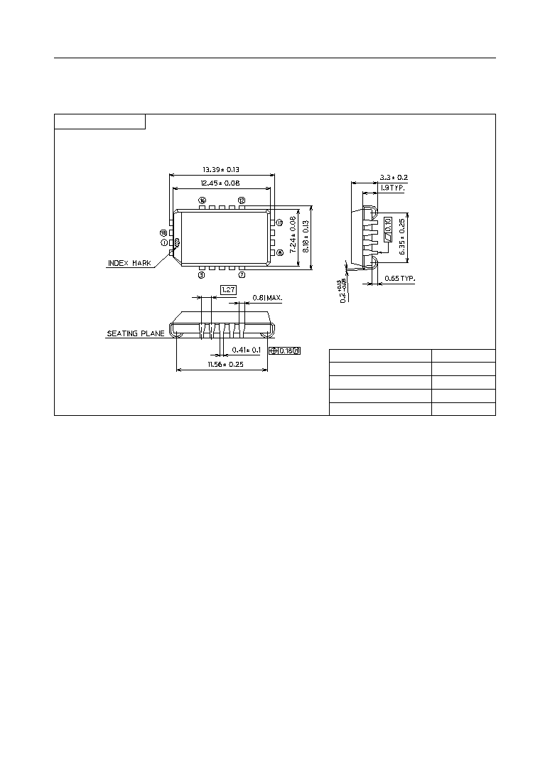
(Unit : mm)
PACKAGE DIMENSIONS
Notes for Mounting the Surface Mount Type Package
The SOP, QFP, TSOP, TQFP, LQFP, SOJ, QFJ (PLCC), SHP, and BGA are surface mount type
packages, which are very susceptible to heat in reflow mounting and humidity absorbed in
storage. Therefore, before you perform reflow mounting, contact Oki's responsible sales person
on the product name, package name, pin number, package code and desired mounting conditions
(reflow method, temperature and times).
Package material
Lead frame material
Pin treatment
Solder plate thickness
Package weight (g)
Epoxy resin
42 alloy
Solder plating
5 mm or more
0.50 TYP.
QFJ18-P-R290-1.27
Spherical surface

NOTICE
1.
The information contained herein can change without notice owing to product and/or
technical improvements. Before using the product, please make sure that the information
being referred to is up-to-date.
2.
The outline of action and examples for application circuits described herein have been
chosen as an explanation for the standard action and performance of the product. When
planning to use the product, please ensure that the external conditions are reflected in the
actual circuit, assembly, and program designs.
3.
When designing your product, please use our product below the specified maximum
ratings and within the specified operating ranges including, but not limited to, operating
voltage, power dissipation, and operating temperature.
4.
Oki assumes no responsibility or liability whatsoever for any failure or unusual or
unexpected operation resulting from misuse, neglect, improper installation, repair, alteration
or accident, improper handling, or unusual physical or electrical stress including, but not
limited to, exposure to parameters beyond the specified maximum ratings or operation
outside the specified operating range.
5.
Neither indemnity against nor license of a third party's industrial and intellectual property
right, etc. is granted by us in connection with the use of the product and/or the information
and drawings contained herein. No responsibility is assumed by us for any infringement
of a third party's right which may result from the use thereof.
6.
The products listed in this document are intended for use in general electronics equipment
for commercial applications (e.g., office automation, communication equipment,
measurement equipment, consumer electronics, etc.). These products are not authorized
for use in any system or application that requires special or enhanced quality and reliability
characteristics nor in any system or application where the failure of such system or
application may result in the loss or damage of property, or death or injury to humans.
Such applications include, but are not limited to, traffic and automotive equipment, safety
devices, aerospace equipment, nuclear power control, medical equipment, and life-support
systems.
7.
Certain products in this document may need government approval before they can be
exported to particular countries. The purchaser assumes the responsibility of determining
the legality of export of these products and will take appropriate and necessary steps at their
own expense for these.
8.
No part of the contents cotained herein may be reprinted or reproduced without our prior
permission.
9.
MS-DOS is a registered trademark of Microsoft Corporation.
Copyright 1999 Oki Electric Industry Co., Ltd.
Printed in Japan
E2Y0002-29-11