
OC48 Optical Receiver w/ CDR for DWDM
OAR25310 Series
Document Number QPS-2001-008
August 2002
Oki Electric Industry
1
OAR25310 Series
Part Number
OAR25310 x ≠ yy - zz
Modification History
Rev. Date
Originator
Comments,
Modifications
DRAFT0.1 Dec.20.2001 T.
IDA
DRAFT0.2 Dec.26.2001 T.
IDA
Specifications optimized for LV
operation
DRAFT0.3
Jan. 08. 2002
H.Ishizaki
Modification of Pin.Description
DRAFT0.4
Jan. 17. 2002
H.Ishizaki
Addition of Fig 1.1 Data/Clock Delay
DRAFT0.5
Aug. 27. 2002
Y.ARAI
Features
-High sensitivity < -28dBm @2000ps/nm.OSNR=23dB
-Integrated APD High Voltage Bias and Control Circuits.
-Adjustable Slice Level : +/-100mV.
-OIL monitor and LOS alarm available.
-High accuracy log converted by OIL function.
-Selective DATA rate function (OC-3/OC-12/OC-48(w/, w/o FEC) and Gb-Ether)
Application
-SONET and ITU-T compliant at OC3, OC12, Gb-Ether, OC48 and w/ FEC for
DWDM
1.
Specifications
Table 1.1 Specifications
(
Vcc =+3.3V+/-5%,Tc=-5 to 75C)
Parameter Unit
Values
Operating Wavelength
nm
1200 to 1600
Maximum Operating Bit rate
Gbps
< 2.488
Minimum Sensitivity dBm
< -28@2000ps/nm, OSNR23dB, PN31-1th
Minimum Overload
dBm
> -8
Jitter Characteristics
-
ITU-T G.958 Conformity
Los off signal activation BER
-
>1E-3
Los off signal deactivation BER
-
>1E-5
Loss of signal response time
usec
Activation<100, Deactivation<250
Power consumption W
< 1.6
Operating case temperature range C
-5
to +75
Operating humidity
%
0 to 85
Dimension
mm
35. 6 x 59 x 8. 9
Reliability Fit
2100 @Tc=45C
Document Number QPS-2001-008
Revision 0.5
DATE: Aug. 27, 2002
Author Y.ARAI
Project Manager K. YUSA

OC48 Optical Receiver w/ CDR for DWDM
OAR25310 Series
Document Number QPS-2001-008
August 2002
Oki Electric Industry
2
Table 1.2 Absolute Maximum Ratings
Parameter Symbol
Condition
Min
Max
Unit
Supply voltage Vcc +5V pin
Vcc
-0.5
+6
V
Maximum signal output current (Clock/Data)
Io
Tc=+25C
0
30
mA
Maximum signal output current (LOS pin)
I
O
-
-25
+25
mA
Operating case temperature range
T
OP
-20
+85
C
Storage temperature range
T
STG
-40
+85
C
Lead soldering temperature/time
-
- 260/10 C/s
Tensile strength of fiber pigtail cable
-
Tc=+25C
-
500
g
Minimum bending radius of fiber pigtail cable
-
30
mm
Table 1.3 Electrical Specifications (
Vcc=+/-5%,
Tc=25C)
Parameter Symbol
Min
Typ
Max
Unit
Power supply voltage (OAR25310-LV)
Vcc
+3.14
+3.30
+3.47
V
Power supply voltage (OAR25310-NV)
Vcc
+4.75
+5.00
+5.25
V
Power supply current
I
CC
- 300 450
mA
Single end
Vout-single
200 - 800
mVp-p
Data/Clock Output
Amplitude
Differential
Vout-diff.
400 1600
Output impedance
R
INRoad
-
50
- ohm
Loss of Signal
V
ON
0 - +0.8
V
LOS signal Output (LOSP)
On Signal
V
LOS
2.4
- Vcc V
Clock/Data delay (Fig1.1)
-
-75
+75
ps
DATA/Clock Pulse width distortion
-
80
100
120
%
75ps
Do(+)
Cko(+)
75ps
75ps 75ps
Figure 1.1 Clock/Data Delay

OC48 Optical Receiver w/ CDR for DWDM
OAR25310 Series
Document Number QPS-2001-008
August 2002
Oki Electric Industry
3
Voltage(V)
Optical Input Power(dBm)
2.85
0.85
-30
-10
Figure 1.2 Optical Input Light Voltage
2.
Block Diagram
Figure 2.1 Block Diagram
APD Bias
Controller
CDR
Pre Amp.
APD
LOS
IN
DATA P
DATA N
Clock P
Clock N
OILV
DVT
OC48 Optical Receiver w/ CDR for DWDM
OAR25310 Series
Document Number QPS-2001-008
August 2002
Oki Electric Industry
4
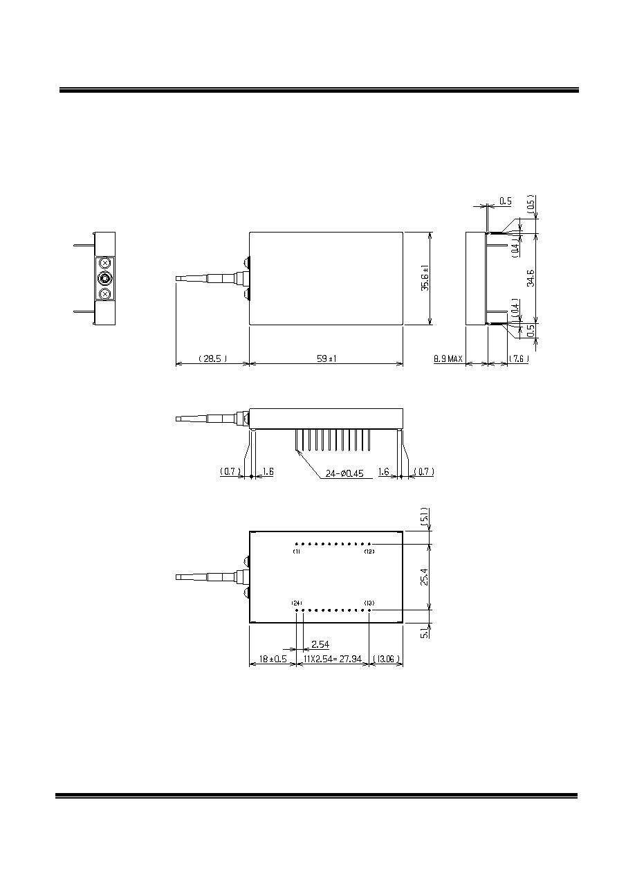
3.
Package Outline (Unit : mm)
Figure 3.1 Package Outline

OC48 Optical Receiver w/ CDR for DWDM
OAR25310 Series
Document Number QPS-2001-008
August 2002
Oki Electric Industry
5
4.
Pin Descriptions
Table 4.1 pin Descriptions
No.
Symbol Functionality
No. Symbol Functionality
01
SEL0
Data rate select (*2)
13
DTV
Decision Threshold Voltage (*1)
02
SEL1
Data rate select (*2)
14
GND
Ground
03
LOS
Loss of Signal
15
GND
Ground
04 GND
Ground
16 GND
Ground
05
Cko(-)
False clock output
17
GND
Ground
06
Cko(+)
True clock output
18
NIC
Not Internally Connected
07 GND
Ground
19 GND
Ground
08
VCC
Positive power supply (*3)
20
GND
Ground
09 GND
Ground
21 NUC
Not
Internally
Connected
10
Do(+)
True data output
22
VCC
Positive power supply (*3)
11
Do(-)
False data output
23
OILV
Optical Input Light Voltage
12 GND
Ground
24 SEL2
Data
select
(*2)
(*1) DTV should be connected to the resistor that is terminated to GND if adjustment is necessary.
(*2) Data rate select function as follows :
SEL0 SEL1 SEL1
Rate
Frequency
0
0
1
OC48 w/ FEC
2.666Gbps
0 0
0 OC48
2.48832
Gbps
1
0
0
Gigabit Ethernet
1.25 Gbps
0 1
0 OC12
622.08Mbps
1 1
0 OC3
155.52Mbps
(*3) OAR25310-NV : Vcc=+5.0V, OAR25310-LV Vcc=3.3V