 | –≠–ª–µ–∫—Ç—Ä–æ–Ω–Ω—ã–π –∫–æ–º–ø–æ–Ω–µ–Ω—Ç: OAR25320 | –°–∫–∞—á–∞—Ç—å:  PDF PDF  ZIP ZIP |
OC48 Optical Receiver w/ CDR
OAR25320 Series
Document Number QPS-0202-101
February 2003
Oki Electric Industry
1
OAR25320 Series
Part Number
OAR25320 x ≠ yy - zz
Modification History
Rev. Date
Originator
Comments,
Modifications
DRAFT0.1 Feb.03.2003 T.Ida
Features
-High sensitivity
-Integrated APD High Voltage Bias and Control Circuits.
-Adjustable Slice Level
-OIL monitor and LOS alarm available.
-High accuracy log converted by OIL function.
-Selective DATA rate function (OC-3/OC-12/OC-48(w/, w/o FEC) and Gb-Ether)
Application
-SONET and ITU-T compliant at OC3, OC12, Gb-Ether, OC48 and w/ FEC for
DWDM
1.
Specifications
Table 1.1 Specifications
(
Vcc =+5.0V+/-5%,Tc=-5 to 75C)
Parameter Unit
Values
Operating Wavelength nm
1200
to
1620
Maximum Operating Bit rate
Gbps
2.666057
Minimum Sensitivity dBm
-28 (Note)
Minimum Overload
dBm
-7
Jitter Characteristics
-
ITU-T G.958 Conformity
Los off signal activation BER
-
>1E-3
Los off signal deactivation BER
-
>1E-5
Loss of signal response time
usec
Activation<100, Deactivation<250
Power consumption W
< 3.0
Operating case temperature range C
-5
to +75
Operating humidity
%
0 to 85
Dimension
mm
35. 6 x 59 x 8. 9
Reliability Fit
1200 @Tc=45C
Note If not specified then measurement conditions are NRZ2
31
-1,Mark Ratio 1/2,BER 1x10
-12
,1550nm
Document Number QPS-0202-101
Revision 0.1
DATE: Feb. 03, 2003
Author T.Ida
Project Manager K. YUSA
OC48 Optical Receiver w/ CDR
OAR25320 Series
Document Number QPS-0202-101
February 2003
Oki Electric Industry
2
Table 1.2 Absolute Maximum Ratings
Parameter Symbol
Condition
Min
Max
Unit
Supply voltage Vcc +5V pin
Vcc
-0.5
+6
V
Maximum signal output current (Clock/Data)
Io
Tc=+25C
0
30
mA
Maximum signal output current (LOS pin)
I
O
-
-25
+25
mA
Operating case temperature range
T
OP
-20
+85
C
Storage temperature range
T
STG
-40
+85
C
Lead soldering temperature/time
-
- 260/10 C/s
Tensile strength of fiber pigtail cable
-
Tc=+25C
-
500
g
Minimum bending radius of fiber pigtail cable
-
30
mm
Table 1.3 Electrical Specifications (
Vcc=+/-5%,
Tc=25C)
Parameter Symbol
Min
Typ
Max
Unit
Power supply voltage (OAR25320-LV)
Vcc
+3.14
+3.30
+3.47
V
Power supply voltage (OAR25320-NV)
Vcc
+4.75
+5.00
+5.25
V
Power supply current
I
CC
- 460 600
mA
Single end
Vout-single
200
-
800
mVp-p
Data/Clock Output
Amplitude
Differential Vout-diff. 400
1600
Output impedance
R
INRoad
-
50
- ohm
On Signal
V
ON
0 - +0.8
V
LOS signal Output (LOS)
Loss of Signal
V
LOS
2.4
- Vcc V
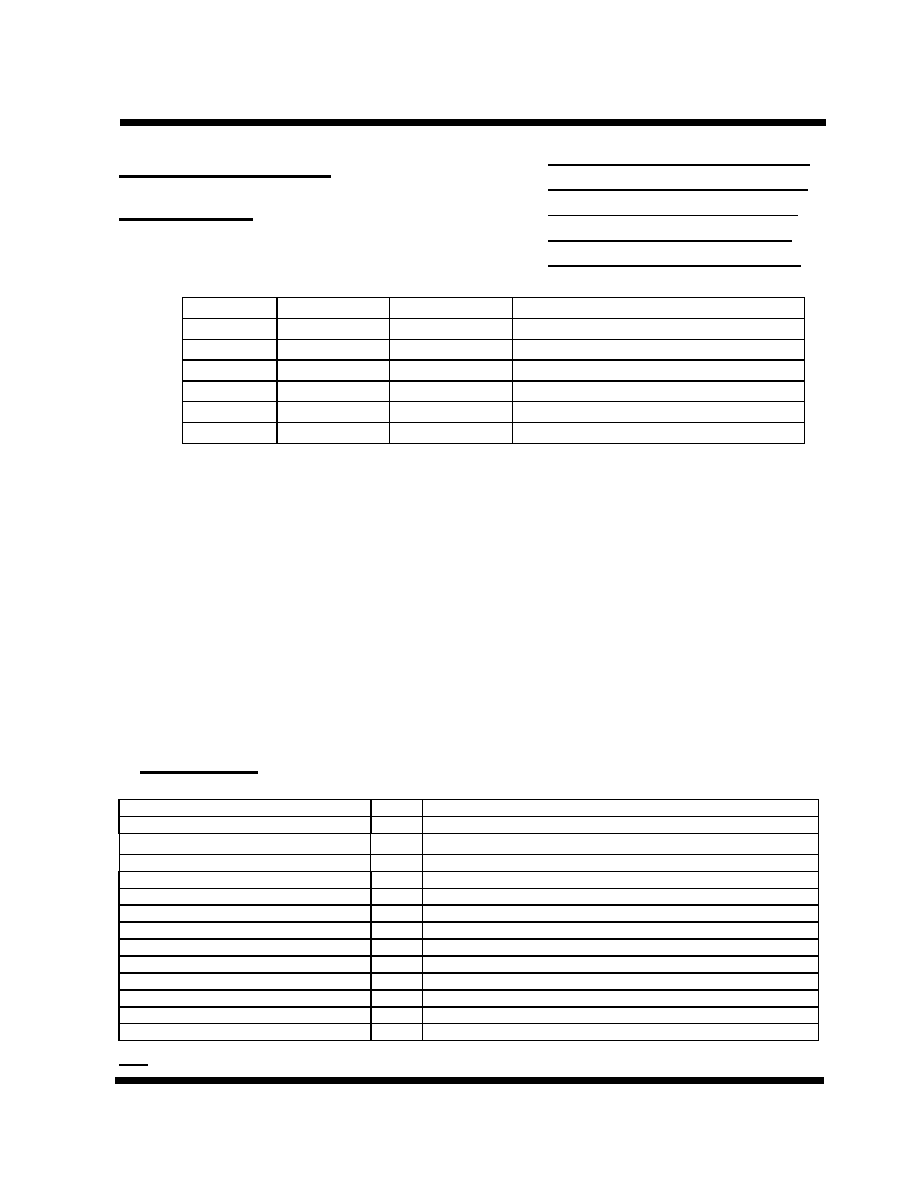
Clock/Data delay (Fig1.1)
-
-75
+75
ps
DATA/Clock Pulse width distortion
-
80
100
120
%
75ps
Do(+)
Cko(+)
75ps
75ps 75ps
Figure 1.1 Clock/Data Delay
OC48 Optical Receiver w/ CDR
OAR25320 Series
Document Number QPS-0202-101
February 2003
Oki Electric Industry
3
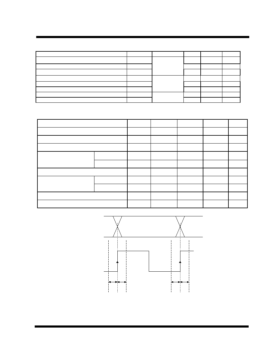
Voltage(V)
Optical Input Power(dBm)
2.85
0.85
-30
-10
Input Power [dBm]
-10
-15
-20
-25
-30
Voltage [V]
2.85
± 0.3
2.35
± 0.3
1.85
± 0.3
1.35
± 0.3
0.85
± 0.3
Figure 1.2 Optical Input Light Voltage
2.
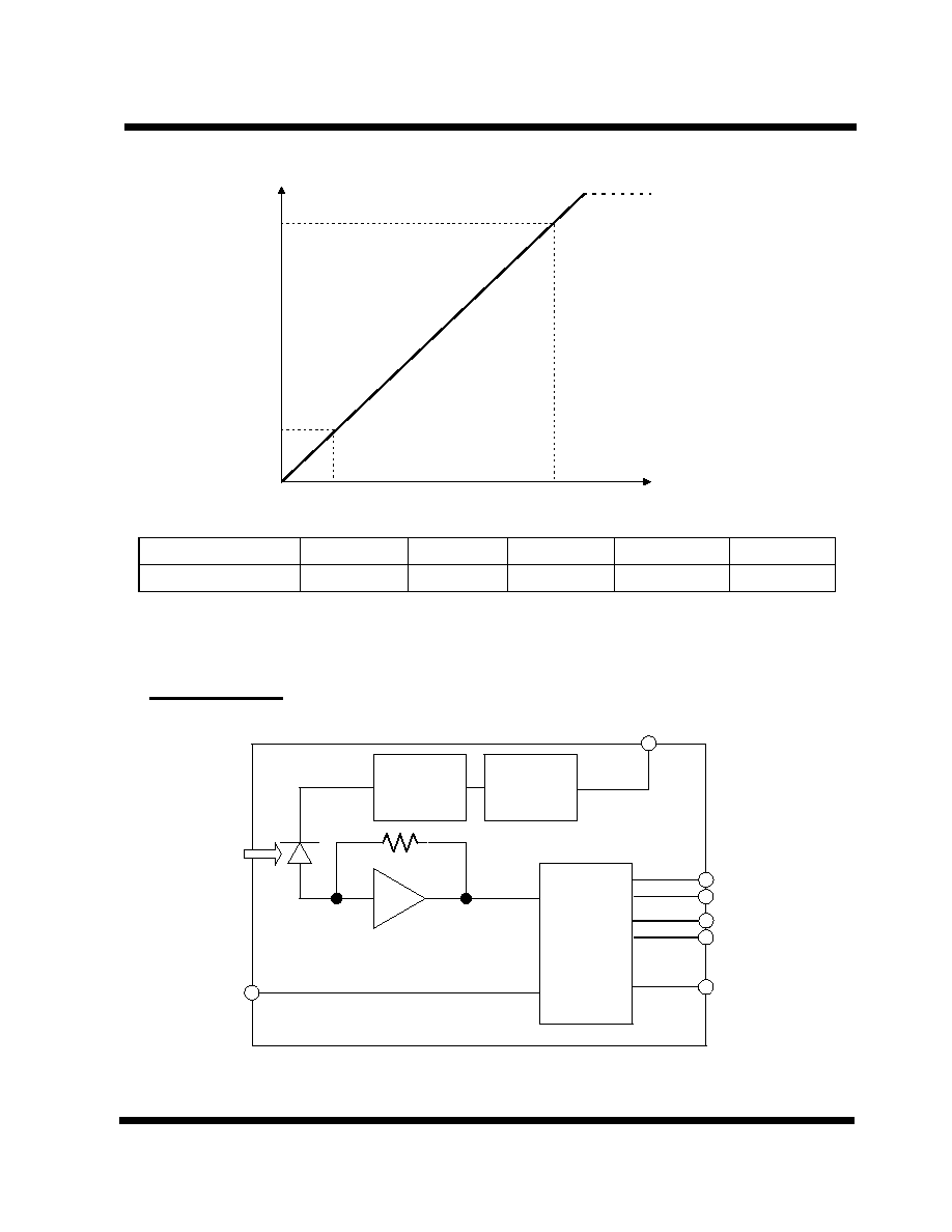
Block Diagram
Figure 2.1 Block Diagram
APD Bias
Controller
CDR
Pre Amp.
APD
LOS
IN
DATA P
DATA N
Clock P
Clock N
OILV
DVT
OC48 Optical Receiver w/ CDR
OAR25320 Series
Document Number QPS-0202-101
February 2003
Oki Electric Industry
4
3.
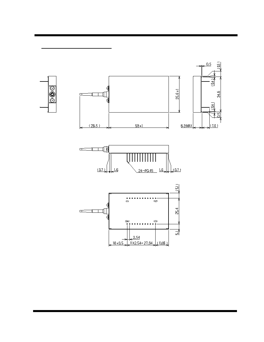
Package Outline (Unit : mm)
Figure 3.1 Package Outline

OC48 Optical Receiver w/ CDR
OAR25320 Series
Document Number QPS-0202-101
February 2003
Oki Electric Industry
5
4. Pin Descriptions
Table 4.1 pin Descriptions
No. Symbol
Functionality
No. Symbol Functionality
01
SEL0
Data rate select (*2)
13
DTV
Decision Threshold Voltage (*1)
02
SEL1
Data rate select (*2)
14
GND
Ground
03
LOS
Loss of Signal
15
GND
Ground
04 GND
Ground
16 GND
Ground
05
Cko(-)
False clock output
17
GND
Ground
06
Cko(+)
True clock output
18
NIC
Not Internally Connected
07 GND
Ground
19 GND
Ground
08
VCC
Positive power supply (*3)
20
GND
Ground
09
GND
Ground
21
NUC
Not Internally Connected
10 Do(+)
True
data
output
22 VCC
Positive power supply (*3)
11
Do(-)
False data output
23
OILV
Optical Input Light Voltage
12
GND
Ground
24
SEL2
Data select (*2)
(*1) DTV should be connected to the resistor (2k
) that is terminated to GND.
(*2) Data rate select function as follows :
SEL0 SEL1 SEL1
Rate
Frequency
0 0
1 OC48
w/
FEC 2.666Gbps
0 0
0 OC48
2.48832
Gbps
1
0
0
Gigabit Ethernet
1.25 Gbps
0 1
0 OC12
622.08Mbps
1 1
0 OC3
155.52Mbps
(*3) OAR25320-NV : Vcc=+5.0V, OAR25320-LV Vcc=3.3V