2.5Gb/s Optical Transmitter for DWDM
OAS25322 Series
Document Number QPS-0202-053
August 2002
Oki Electric Industry
1
OAS25322 Series
Part Number
OAS25322x-NV-WDM-yy-zz
Modification History
Rev. Date
Originator
Comments,
Modifications
Features
-Center Wavelength range: 1528.77 to 1563.86nm ITU-T G.692 100GHz channel
spacing
-High output Power +1dBm(Typ)
-Operation speed 150M to 2.7Gbps
-Selection of Clocked or non-clocked operation
-Selection of wavelength 1ch sifting
-Supply voltage: +3.3V and +5V
Application
-SONET and ITU-T compliant at OC-48 and STM-16 and FEC for DWDM
Document Number QPS-0202-052
Revision 0.1
DATE: Aug. 27, 2002
Author T.Arai
Project Manager K. YUSA
2.5Gb/s Optical Transmitter for DWDM
OAS25322 Series
Document Number QPS-0202-053
August 2002
Oki Electric Industry
2
1.
Specifications
Table 1.1 Specifications
(
Vcc =+5.0V�5%,Tc=0 to 70�C)
Parameter Unit
Values
Mean launched power range
dBm
0 to +2
Maximum Operating Bit Rate
Gbps
2.488
Center wavelength range
nm
1528.77 to 1563.86
Wavelength channel spacing
ITU-T G.692 100GHz channel spacing
Center wavelength accuracy
nm
� 0.015
Variation center wavelength over temperature
nm
� 0.05
Maximum spectral width [20dB down]
nm
0. 3(Typ) , 0. 5(Max)
Minimum side mode suppression ratio
dB
30
Center wavelength aging BOL to EOL
nm
� 0.1
Minimum extinction ratio
dB
8.2
Optical output waveform
Meets for ITU-T G.957
Maximum Fiber Dispersion
ps/nm
3200
Dispersion penalty dB
2
Power consumption W
5
Operating case temperature range �C
Tc=0
to+70
Operating humidity %
0
to
85
Dimension
mm
73.4 x 51 x 12.7
Table 1.2 Absolute Maximum Ratings
Parameter Symbol
Condition
Min
Max
Unit
Supply voltage Vcc +5V pin
Vcc
-0.5
+7
V
Supply voltage VTEC+3.3V pin
VTEC
Tc=+25�C
-0.5 +4.6 V
Maximum signal input voltage (Clock/Data)
V
I
0
Vcc
V
Maximum signal output current (TDA pin)
I
O
-
-25 +25 mA
Operating case temperature range
T
OP
-20
+85
�C
Storage temperature range
T
STG
-40
+85
�C
Lead soldering temperature/time
-
- 260/10 C/s
Tensile strength of fiber pigtail cable
-
Tc=+25�C
-
500
g
Minimum bending radius of fiber pigtail cable
-
30
mm

2.5Gb/s Optical Transmitter for DWDM
OAS25322 Series
Document Number QPS-0202-053
August 2002
Oki Electric Industry
3
Table 1.3 Electrical Specifications (Vcc =+5.0V�5%,Tc=+25�C)
Parameter Symbol
Min
Typ
Max
Unit
Power supply voltage
Vcc
+4.75
+5.00
+5.25
V
Power supply current
I
CC
- 350 400
mA
TEC power supply Voltage
V
TEC
+3.0 +3.3 +3.5 V
TEC power supply current
I
TEC
- 0.4 1.0
A
Single end
Vin-single
250 - 1300
Data/Clock Input Amplitude
[AC- Coupled at Internal]
Differential
Vin-diff.
125 650
mVp-p
Input impedance
R
INRoad
-
50
- ohm
Clocked
V
CLK ON
0
- +0.8 V
Clock mode Select input
Voltage
Non
Clocked
V
NON CLK
2.0 - Vcc
V
n
V
n
0 -
+0.8
V
Wavelength Selection input
Voltage
n-1
V
n-1
2.0 - Vcc
V
Enable
V
EN
0 - +0.8
V
Shut Down input Voltage
Disable
V
DIS
2.0 - Vcc V
Normal V
OL
0 - +0.3
V
Deviation
V
OH
+4.5
Vcc V
TEC Temperature deviation error
Monitor (Active High)
Setting
Level
alarm
-1 +1
C
V
OL
0 - +0.3
V
Laser Degrade Alarm (Active Low)
3
V
OH
+4.5 - Vcc V
LD Bias monitor
3
V
LBM
- 20 -
mV/mA
Back facet Monitor
V
BF
- 500 -
mV/mW
DATA/CLOCK input Rise/Fall time
1
t
R
/t
F
- - 0.12
ns
DATA/CLOCK timing
2
ts/th
50
-
-
psec
Input Clock Pulse width distortion
-
40
50
60
%
1. Between 20% and 80%
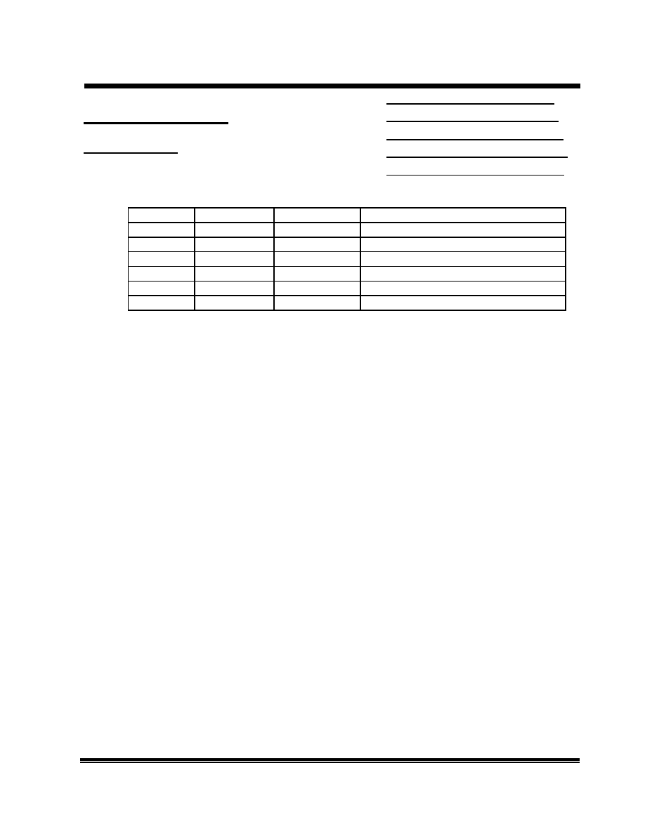
2.
The data and clock timing diagram is Figure 1.1
3.
See Table 4.1
2.5Gb/s Optical Transmitter for DWDM
OAS25322 Series
Document Number QPS-0202-053
August 2002
Oki Electric Industry
4
50ps
Admitted range of
Cki(+) rise-edge
Di(+)
Cki(+)
50ps
50ps 50ps
ts
th
Figure 1.1 Data/Clock Timing Diagram
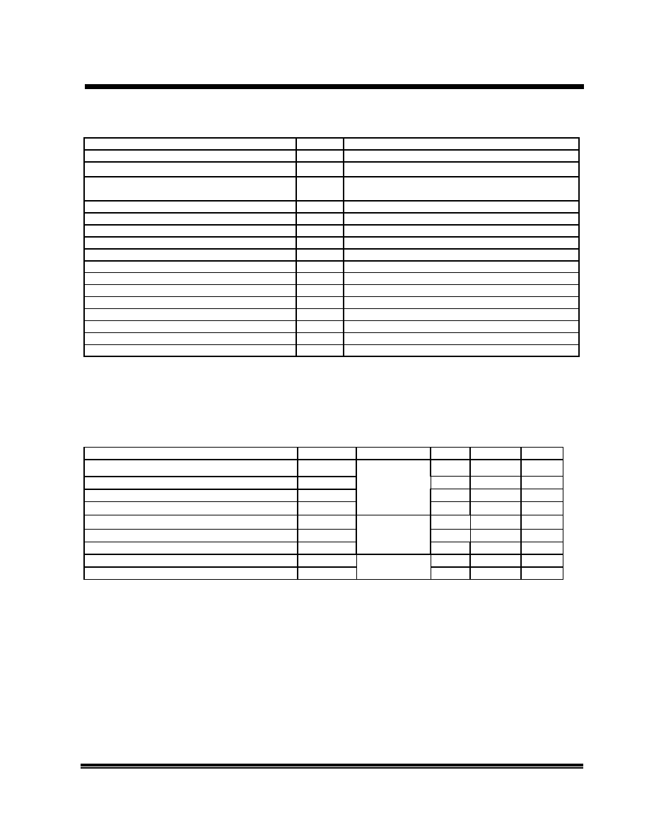
2.
Block Diagram
True data input
Wavelength Selection Command
True clk input
LD Driver
APC
Temperature Deviation Alarm
Back facet monitor
False clk input
False data input
LD Module
Clock select
ATC
Laser Bias Monitor
Or
Laser Degraed Alarm
Shut down
OPT OUT
D-F/F
Figure 2.1 Block Diagram

2.5Gb/s Optical Transmitter for DWDM
OAS25322 Series
Document Number QPS-0202-053
August 2002
Oki Electric Industry
5
3.
Package Outline (Unit : mm)
Figure 2.2 Package Outline