FEDFOAS2531-01
Electronic Components
This version: Aug.
2000
OAS2531-LV, OAS2532-LV, OAS2536-LV, OAS2537-LV
OAR2531-LV, OAR2535-LV
2.5Gb/s Optical Module Operating at 3.3 V
APPLICATION
∑ Optical transmitter/receiver for 2.4888Gb/s (STM-16/OC-48)
FEATURES
∑ STM-16/OC-48 compatible
∑ CDR function
∑ +3.3 V single power supply
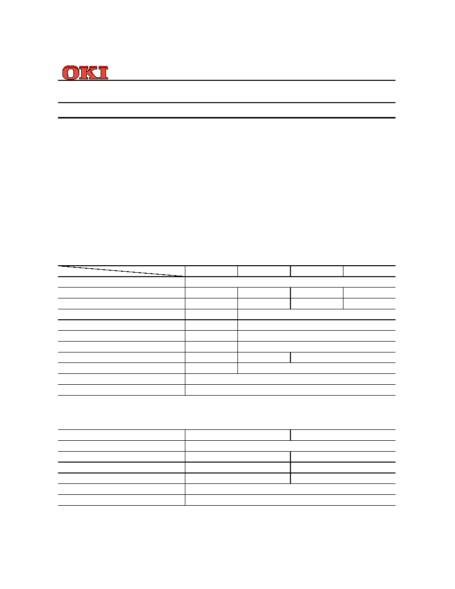
SPECIFICATION
[Transmitter]
OAS2531-LV
OAS2532-LV
OAS2536-LV
OAS2537-LV
Bit rate
(Mb/s)
2488.32
Optical wavelength
(nm)
1266 to 1360
1260 to 1360
1280 to 1335
1500 to 1580
Optical output power
(dBm)
--10 to --3
--5 to 0
--2 to +3
--2 to +3
RMS spectral width
(nm)
4
Spectral width [
20dB down] (nm)
1
Side mode suppression ratio
(dB)
30
Extinction ratio
(dB)
8.2
8.2
Power consumption
(W)
0.6
0.7
0.8
Laser diode
FP-LD
DFB-LD
Operating temperature
(
∞C)
--20 to 85
Dimension (mm)
25
◊ 55 ◊ 12.5
[Receiver]
OAR2531-LV
OAR2535-LV
Bit rate
(Mb/s)
2488.32
Optical input power [
EBR = 10
-10
] (dBm)
--18 to 0
--28 to --9
Power consumption
(W)
0.7
0.9
Photo diode
PIN-PD
APD
Operating temperature
(
∞C)
--20 to 85
Dimension
(mm)
30
◊ 70 ◊ 11.1

FEDFOAS2531-01
1
Electronic Components
[Receiver]
PIN DESCRIPTIONS
[Transmitter]
[Receiver]
No.
Symbol
Functionality
No.
Symbol
Functionality
01
V
CC
Power supply
(V
CC
= +3.3 V)
01
NC
No user connection
02
V
CC
Power supply
(V
CC
= +3.3 V)
02
GND
Ground
03
LBFM (+)
Laser back face monitor (+)
03
NC
No user connection
04
LBFM (--)
Laser back face monitor (--)
04
GND
Ground
05
DATA
Negative data input
(LVPECL)
05
DATA
Negative data output
(CML)
06
NC
No user connection
06
DATA
Positive data output
(CML)
07
DATA
Positive data input
(LVPECL)
07
GND
Ground
08
NC
No user connection
08
GND
Ground
09
V
CC
Power supply
(V
CC
= +3.3 V)
09
CLK
Negative clock output
(CML)
10
V
CC
Power supply
(V
CC
= +3.3 V)
10
CLK
Positive clock output
(CML)
11
GND
Ground
11
GND
Ground
12
GND
Ground
12
GND
Ground
13
GND
Ground
13
V
CC
Power supply
(V
CC
= +3.3 V)
14
GND
Ground
14
V
CC
Power supply
(V
CC
= +3.3 V)
15
TD
Laser bias alarm output
(LVTTL/LVCMOS)
15
V
CC
Power supply
(V
CC
= +3.3 V)
16
LS
Transmitter disable input
(LVTTL/LVCMOS)
16
V
CC
Power supply
(V
CC
= +3.3 V)
17
Latch
Select latched or non latched data with
clock
(LVTTL/LVCMOS)
17
GND
Ground
18
CLK
Positive clock input
(LVPECL)
18
GND
Ground
19
NC
No user connection
19
GND
Ground
20
CLK
Negative clock input
(LVPECL)
20
GND
Ground
21
LBCM (--)
Laser bias current monitor (--)
21
LOS
Positive Loss of signal alarm output
(LVTTL/LVCMOS)
22
LBCM (+)
Laser bias current monitor (+)
22
LOS
Negative Loss of signal alarm output
(LVTTL/LVCMOS)
23
V
CC
Power supply
(V
CC
= +3.3 V)
23
V
CC
Power supply
(V
CC
= +3.3 V)
24
V
CC
Power supply
(V
CC
= +3.3 V)
24
V
CC
Power supply
(V
CC
= +3.3 V)
Bottom view
Side view
0.5 2.54
27.94
3.1
11.1
18.54
(01)
(12)
(13)
(24)
20.32
4.84
4.84
30.0
70.0

FEDFOAS2531-01
1
Electronic Components
NOTICE
1.
The information contained herein can change without notice owing to product and/or technical
improvements. Before using the product, please make sure that the information being referred to is up-to-
date.
2.
The outline of action and examples for application circuits described herein have been chosen as an
explanation for the standard action and performance of the product. When planning to use the product,
please ensure that the external conditions are reflected in the actual circuit, assembly, and program designs.
3.
When designing your product, please use our product below the specified maximum ratings and within the
specified operating ranges including, but not limited to, operating voltage, power dissipation, and operating
temperature.
4.
Oki assumes no responsibility or liability whatsoever for any failure or unusual or unexpected operation
resulting from misuse, neglect, improper installation, repair, alteration or accident, improper handling, or
unusual physical or electrical stress including, but not limited to, exposure to parameters beyond the
specified maximum ratings or operation outside the specified operating range.
5.
Neither indemnity against nor license of a third par ty s industrial and intellectual property right, etc. is
granted by us in connection with the use of the product and/or the information and drawings contained
herein. No responsibility is assumed by us for any infringement of a third party s right which may result
from the use thereof.
6.
The products listed in this document are intended for use in general electronics equipment for commercial
applications (e.g., office automation, communication equipment, measurement equipment, consumer
electronics, etc.). These products are not authorized for use in any system or application that requires
special or enhanced quality and reliability characteristics nor in any system or application where the failure
of such system or application may result in the loss or damage of property, or death or injury to humans.
Such applications include, but are not limited to, traffic and automotive equipment, safety devices,
aerospace equipment, nuclear power control, medical equipment, and life-support systems.
7.
Certain products in this document may need government approval before they can be exported to particular
countries. The purchaser assumes the responsibility of determining the legality of export of these products
and will take appropriate and necessary steps at their own expense for these.
8.
No part of the contents contained herein may be reprinted or reproduced without our prior permission.
Copyright 2000 Oki Electric Industry Co., Ltd.
